an author's https://oatao.univ-toulouse.fr/21812
https://doi.org/10.1109/TED.2017.2762433
Marcelot, Olivier and Goiffon, Vincent and Rizzolo, Serena and Pace, Federico and Magnan, Pierre Dark Current Sharing and Cancellation Mechanisms in CMOS Image Sensors Analyzed by TCAD Simulations. (2017) IEEE Transactions on Electron Devices, 64 (12). 4985-4991. ISSN 0018-9383
Dark Current Sharing and Cancellation Mechanisms
in CMOS Image Sensors Analyzed by TCAD
Simulations
O. Marcelot, Member, IEEE, V. Goiffon, Member, IEEE, S. Rizzolo, Member, IEEE, F. Pace, Student
Member, IEEE,
and P. Magnan, Member, IEEE
Abstract—TCAD simulations are conducted on a 4T PPD pixel, on a conventional gated photodiode, and finally on a radiation hardened pixel. Simulations consist in demonstrating that it is possible to reduce the dark current due to interface states brought by the adjacent gate, by means of a sharing mechanism between the photodiode and the drain. The sharing mechanism is activated and controlled by polarizing the adjacent gate at a positive off voltage, and consequently the dark current is reduced and not compensated. The drawback of the dark current reduction is a reduction of the full well capacity of the photodiode, which is not a problem when the pixel saturation is limited by the readout chain. Some measurement performed on pixel arrays confirm the TCAD results.
Index Terms—CMOS Image Sensors, CIS, Simulation, Deep Submicron Process, CMOS, pinned photodiode, PPD, Dark current, solid-state image sensor, STI.
I. INTRODUCTION
T
HANKS to the latest technological progress, CMOSImage Sensor (CIS) are now widely used for commercial and scientific applications. The photo-sensitive element is either a conventional photodiode, or a Pinned Photodiode (PPD) [1], [2], [3], and is associated to a readout circuitry based on 3 to 4 and even more transistors [4], the whole forming a pixel. Contrary to conventional photodiodes, pinned photodiodes are built by a buried N-doped layer, which is not in contact with the surface, and a very narrow and highly P-doped layer between the surface and the buried N-layer, preventing any contact between the depletion extension from the photodiode and the oxide, which insures a dramatic dark current reduction compared to conventional photodiodes [3].
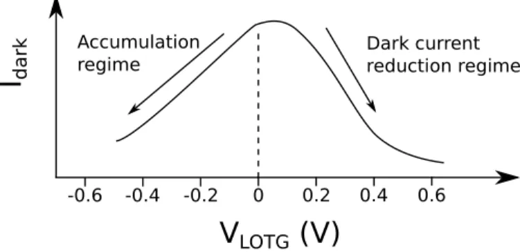
PPDs have been extensively studied in order to understand all the transfer mechanisms between the photodiode and the floating diffusion, the PPD key feature parameters and its access [5], [6], [7]. Although many dark current measurements of pinned photodiodes have been presented, to our knowledge, no study explains and demonstrates the possibility of dark current reduction by sharing mechanisms between adjacent PN junctions. Indeed, if a dark current curve versus the off
Transfer Gate (TG) voltage (VLOTG) is analyzed [8], [9], it
shows 2 different regimes (Fig. 1):
• accumulation regime, at negative VLOTG
• a dark current reduction regime, at positive VLOTG
O. Marcelot, V. Goiffon, S. Rizzolo, F. Pace and P. Magnan are with ISAE, Universit´e de Toulouse, Image Sensor Research Team, 10 avenue E.Belin, F-31055, Toulouse, France. (corresponding e-mail [email protected])
I
darkV
LOTG(V)
0 0.2 0.4 0.6 -0.2 -0.4 -0.6 Accumulation regime Dark current reduction regimeFig. 1. Example of dark current evolution with the transfer gate off voltage (VLOTG). Two main regimes are visible: accumulation regime, and a dark current reduction regime
At VLOTG = 0 V, depletion extensions of the PPD and the
transfer gate are merged, leading to a high dark current due
to interface states below the TG. When VLOTG is lowered
to negative values, the transfer gate is accumulating, and the depletion region of the PPD does not reach the interface states below the TG any more. Therefore, dark current is highly
reduced. If VLOTG is too low, the TG accumulation may
extend into the PPD vicinity, and it may lead to a high leakage current called Gate Induced Drain Leakage (GIDL), similar to
the one found in MOSFET [10]. For positive VLOTGvalues, a
dark current reduction can be observed, and can be even more important than during the TG accumulation regime.
The purpose of this work is to demonstrate that a dark
current reduction is possible at positive VLOTG, and does not
consist in a dark current compensation. To do so, TCAD simu-lations will be conducted on a 4T PPD, in order to analyze the dark current electron displacements and the eventual parasitic collection by the positive transfer gate off voltage. Then, other applications of this dark current reduction will be presented, like conventional 3T photodiode and radiation hardened pixels. First of all, and for a better understanding, conventional dark current sources of 4T PPD pixels are given.
II. DIFFERENT DARK CURRENT SOURCES
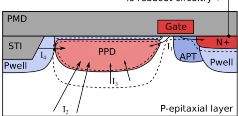
In a 4T photodiode, several dark current sources may be identified. One can describe the following current contribu-tions [11], [12], [13], [14] (Fig. 2):
• interface states generation at the Silicon - Oxide interface
PMD Gate N+ STI Pwell PPD I1 I4 I3 I2 P-epitaxial layer Pwell To readout circuitry APT
Fig. 2. Schematic view of a 4T PPD pixel showing the different dark current contributions. The readout circuitry is not shown (reset transistor, source follower, row selector), and APT is for the Anti-Punch Through implantation. The dashed lines represent the depletion extension of the photodiode, for a depleted transfer gate. In order to illustrate the dark current sharing mechanism, the I1 current generated under TG is shared between the PPD and the FD.
• minority carrier diffusion from the bulk (I2)
• electron-hole pair generation in the depletion region (I3)
• sidewalls and edges of Shallow Trench Isolation (STI)
(I4), and PMD
In a pinned photodiode, the pinned layer prevents any contact between the depletion extension of the photodiode and the surface, avoiding interface states generation dark current. However if the transfer gate is in depletion regime, the depleted TG channel merges with the photodiode depletion extension and an intense dark current due to interface states
appears (I1). The electron-hole pair generation in the space
charge region is supposed to be low, because of the very
weak defects concentration (I3). Subsequently, the impact
of sidewalls and edges of STI is negligible because of the depletion extension which is not supposed to merge with the STI due to the Pwell passivation.
In a pinned photodiode operated with an Anti-Blooming (AB) gate, the main dark current contributor remains the interface states at the silicon - oxide interface under the gate. It is proposed to study this contribution in this paper using a
positive VLOTG, as described in the following parts.
III. STUDY OF4T PPDDARK CURRENT REDUCTION BY
SHARING MECHANISMS A. Principle of the sharing mechanism
Exchange of charge by means of punch-through mecha-nisms between adjacent and depleted nodes have been already studied for more and fully-depleted photodiodes array in very high resistive substrates [15], [16]. In these papers, the depletion extension of adjacent photodiodes in highly resistive substrate may be merged and therefore leads to leakage current between photodiodes, depending on the potential barrier along the leakage path and the photodiode potential. Consequently, electrons stored in adjacent photodiodes are shared until an equilibrium is reached. In these applications this phenomenon has to be avoided. In our case, dark current electrons generated under the gate in the depleted channel are shared between the drain and the photodiode, but unlike the punch-through
TG RS PPD
Pwell APT
FD
Fig. 3. TCAD doping distribution of the 4T simulated PPD showing the dif-ferent layers: PPD, Transfer Gate (TG), Reset Gate (RS), Pwell implantation, Anti-Punch Through (APT) implantation. FD is the Floating Diffusion.
phenomenon, integrated electrons in the PPD and electrons in the FD are not shared.
In a 4T photodiode, the TG is put in depletion for positive
VLOTGin off state. The photodiode depletion extension merges
with the TG depletion region and the floating diffusion deple-tion region. Thus, the dark current generated by interface states under the TG can be shared between the photodiode (as it is generally the case) and the floating diffusion (Fig. 2), which leads to a dark current reduction. In this situation the floating diffusion does not directly collect photo-generated electrons thanks to the Anti-Punch Through (APT) implantation, but may discharge the photodiode by means of a punch-through current, depending on the potential barrier between the PPD and the FD. The ratio of dark current captured by the floating diffusion over the total dark generated current depends on
the VLOTG voltage, as long as the floating diffusion does not
collect photo-generated electrons, which would result in loss of QE.
On the following part, a 4T PPD pixel is studied by means of TCAD simulation, in order to identify the benefits and the drawbacks of the dark current sharing mechanisms.
B. Dark current reduction on a 4T PPD photodiode
A 4T PPD is simulated, using the Synopsys Sentaurus 2015 software. The simulation is performed in two dimensions, and the doping distribution is built from Secondary Ion Mass Spectrometry (SIMS) doping profiles. The electrical study is performed with the Sdevice tool, activating the following models: recombination using Shockley Read Hall with doping dependance, Auger and Band to band. The 2D simulated device is composed of a PPD with its transfer gate and a floating diffusion, and of a reset transistor allowing a floating state of the floating simulated node. The photodiode is 4 µm long, and the 4T PPD device comprises the usual layers [17]: a P+ pinning and a N+ photodiode layer, an APT layer preventing leakage between the PPD and the floating node, a Vt adjust layer in the first part of the TG channel, a N+ layer used for the floating diffusion, and a Pwell isolating the floating diffusion and the reset transistor from the bulk (Fig. 3). Firstly, the PPD is emptied thanks to the activation of the
reset and the transfer gate. Then, the TG is biased at VLOTG,
and the distribution of electron quasi Fermi energy (eQF) is plotted (Fig. 4). The 2D distribution of eQF shows that the potential increases in the TG channel from the PPD side to the FD side, which is favorable to a dark current discharge towards the floating diffusion. Actually, dark current generated in the TG channel at the vicinity of the PPD may be captured by
V_TG=0V V_TG=0.5V V_TG=0.7V PPD PPD PPD FD FD FD
Fig. 4. TCAD electron quasi Fermi energy distribution of the 4T simulated PPD at VLOTG = 0 V, VLOTG= 0.5 V, and VLOTG= 0.7 V. Streamlines driven by the gradient of electron quasi Fermi are also plotted. Each streamline is spaced apart 15 nm, 15 nm under the gate oxide. The red line represents the junction line.
0 2 4 6 8 10 12 14 1.1 1.2 1.3 1.4 1.5 -1 -0.5 0 0.5 1 FW C PP D ( k e -) Dark cu rr e n t (e -) VlowTG (V) e_dark_PPD FW_ppd
Fig. 5. In blue line, TCAD simulation of the amount of dark current electrons integrated in the PPD during 10 µs. A hole trap model is used with a concentration of 5 × 10⁹traps.cm−2 and a capture cross sections of 1 × 10⁻¹⁵cm2. The curve without hole trap model is also shown for comparison. In red dashed line, TCAD simulation of the FWC of the PPD for various VLOTG.
the PPD because the photodiode implantations extend slightly under the TG and the PPD potential competes with the TG channel potential. In the Fig. 4, curves (streamlines) tangents to the gradient of eQF [18] are displayed, because they show the path followed by dark current electrons in the TG channel.
At VLOTG= 0 V, dark current electrons generated in the PPD
vicinity are captured by the PPD. And, by increasing VLOTG
until 0.7 V, all dark current electrons are drained from the gate channel to the floating diffusion: the dark current is reduced. Consequently, increasing the TG polarization increases the channel potential and drives effectively all the dark current, even the part generated in the vicinity of the PPD.
To go further, a dark current integration of the PPD is simulated. In a same way as in [19], a hole trap model in specified in Sdevice and emulates the dark current generation. It is defined at all silicon-oxide interfaces, with a
concen-tration of 5 × 10⁹traps.cm−2 and a capture cross sections
of 1 × 10⁻¹⁵cm2. After emptying the photodiode, the TG is
biased at VLOTG, and the photodiode integrates dark electrons
during 10 µs. The amount of integrated dark electrons is
reported in the Fig. 5 for various VLOTG. The dark current
shape is similar to the one presented in Fig. 1, and shows
0 2 4 6 8 10 12 14 0 5 10 15 20 25 30 35 40 -0.5 0 0.5 1 1.5 Ful l w e ll c a pacit y ( ke -) Da rk cur re n t (e -/ s) VlowTG (V) Dark current V_Sat
Fig. 6. Dark current and full well capacity measurements performed at 22 C on 4T PPD pixels for various VLOTG.
a maximum centered at 0 V. The position of this maximum depends on the process and on the design. Therefore in the
following the increase ∆VLOTG of the off polarization of the
TG will be referenced to the dark current maximum position
VLOTG = 0 V. This result clearly shows a high reduction of
the dark current by increasing ∆VLOTG. For an increase of
0.5 V, the residual amount of electrons in the PPD is even lower than in the accumulation regime, which means that the dark current coming from the interface states of the TG is canceled.
The parasitic collection due to the positive polarization of
VLOTG is also a matter of the greatest concern. In order to
analyze the impact of the sharing mechanism on the parasitic collection, the Full Well Capacity (FWC) of the PPD is
ana-lyzed against VLOTG. Indeed, if the PPD is at the equilibrium
and full of electrons, its potential approaches zero, and by
increasing VLOTG the potential barrier between the PPD and
the floating node disappears, and a leakage current can flow from the PPD to the floating node, performing like an anti-blooming system. As the potential barrier between the PPD and the FD decreases, the saturation level of the PPD decreases as well. In the Fig. 5 the FWC is extracted by monitoring the amount of electrons in the PPD at the beginning of the
simulation, VLOTG being biased and the PPD not reset. For
an increase of ∆VLOTG ≥ 0.3 V, the FWC starts to decrease.
As the FWC reduction is conditioned by the potential barrier mitigation between the PPD and the FD, it may occur at a
different VLOTG compared with the dark current reduction.
Therefore, TCAD simulations have shown that operating the PPD with TG at a positive voltage in off state leads to a cancellation of the dark current coming from the interface states under TG. By doing so, it seems possible to achieve similar or even better dark current reduction compared to PPD operated in accumulation regime, for an increase of
∆VLOTG ≥ 0.5 V. However, the increase of ∆VLOTG to
positive voltage causes a reduction of the FWC of the PPD. This consequence is not a problem if the pixel has a high CVF or if the pixel saturation is limited by the readout circuitry.
C. Measurement of dark current reduction by sharing mech-anism
A dark current measurement is performed on 7 µm 4T PPD pixels implemented in an array, manufactured using a sub-micrometer imaging CMOS process identical to the one used for the TCAD study. The measurement is done at 22 C for
various polarization of VLOTG (Fig. 6).
The maximum dark current is achieved at VLOTG = 0.4 V,
and decreasing VLOTG leads to a dark current reduction, the
TG being accumulated. The dark current reduction occurs
until VLOTG = 0 V from which a plateau is visible. Then, if
VLOTG is increased beyond 0.4 V a dark current reduction by
sharing mechanism is visible. At 0.8 V, the dark current level is comparable to the one achieved in accumulation regime. The same figure also shows the measured full well capacity of the PPD. As it can be seen, for positive polarization of
VLOTG, the saturation level monotonously decreases until
10 % of the Equilibrium FWC (EFWC) at VLOTG = 1.5 V.
At VLOTG = 0.9 V, i.e at ∆VLOTG = 0.5 V, the FWC is at
35 % of the EFWC, which is a bit lower than the TCAD simulation. Compared to the simulation, curves are shifted,
and the PPD saturation decreases for smaller VLOTG. The
root cause is supposed to be the imprecision of the doping profiles simulated in the transfer gate region, as the threshold adjust implantation and the tooling applied on APT and sensor implantations were deducted from experimental observations. Indeed, small variations on these implantation positions or concentrations have strong impacts on charge transfer and PPD FWC [17].
This measurement confirms the TCAD results: increasing
VLOTG at positive voltage leads to a dark current reduction,
and this performance is accompanied by a decrease of the PPD FWC. Again, if the pixel has a high CVF or if the pixel saturation is limited by the readout circuitry saturation, the reduction of FWC is not a particular issue.
IV. OTHER APPLICATIONS OF THE DARK CURRENT
REDUCTION BY SHARING MECHANISM
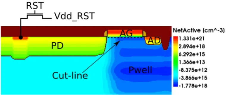
A. Dark current reduction on a conventional 3T photodiode In spite of the development of high performance pinned photodiode, conventional 3T CMOS image sensors are still used for commercial and scientific applications, because they don’t need an advanced CMOS images process, they offer a better full well capacity and the possibility to design large pixel pitches [14], [20] without transfer issue. Therefore, the study of dark current reduction in conventional photodiodes is still an active topic. For instance, some works have been done on the photodiode design by surrounding the pixel by a p-well [21], or by introducing dark current compensation mechanisms [22], [23], [24], [25], [26], [27]. Some of these concepts of dark current compensation consist in subtracting a calibrated dark frame by means of a shielded dummy pixel, or even by controlling a negative feedback using the reset transistor. Hence, these methods rely on the addition of a current in order to compensate the dark current, but they do not reduce the dark current shot noise and the dark current non uniformity. As depleted extremities of conventional 3T
PD Pwell AG AD RST Vdd_RST Cut-line
Fig. 7. TCAD doping distribution of the conventional simulated photodiode showing the different layers: PD, Adjacent Gate (AG), Adjacent Drain (AD), Pwell implantation. The electrical simulation is performed in mixed mode and the schematic of the reset transistor modeled with a spice model is shown.
photodiodes are known dark current sources, one approach is also to use gated diodes [28]. Besides, in [28], the authors show that the dark current of irradiated gated diodes can be reduced by increasing the gate voltage, but they do not go into details concerning what happens on the other side of the gate. On the following, a gated diode is studied, and considering the results previously obtained on a 4T PPD, the concept of dark current reduction by sharing mechanisms is applied on it.
A 2D 5 µm long gated photodiodes is simulated with a 1 µm adjacent gate (called here Adjacent Gate, AG) next to a drain (Adjacent Drain, AD) (Fig. 7). The electrical simulation is performed in Mixed Mode, and a reset transistor allowing a floating state of the photodiode is connected to the conventional photodiode. The spice model of the reset transistor is the one given by the founder. Firstly, a reset phase is applied to the photodiode by means of the reset transistor, and the adjacent drain is biased at 3.3 V. Then, the adjacent
gate is biased at VAG.
In order to analyze the lateral electric field distribution in the gate channel, a cross-section along a cut-line 15 nm below the surface oxide from the left side to the right side of the AG is performed (see the representation of the cut-line in Fig. 7).
The cross-sections of the lateral electric field for various VAG
are shown in the Fig. 8. The gate channel is divided into two sections in which the electric field opposes. Indeed, even at
VAG= 0 V, a potential gradient tends to push the charge to the
photodiode in the left part of the gate channel, and from about L = 0.45 - 0.5 µm, the point where the electric field polarity changes, and another potential gradient drives the charge to the adjacent drain. By increasing the adjacent gate voltage, the lateral electric field grows from negligible values to about 500 V/cm all along the gate channel until the drain, which should efficiency lead the dark current electrons towards the drain.
As in the part dealing with the 4T PPD, a dark current integration of the PPD is simulated by means of the intro-duction of a hole trap model at the silicon-oxide interface. The same trap model parameters are used and the net excess of dark electrons generated by the trap model is plotted in the Fig. 9. The simulation clearly shows a high reduction
of the dark current by increasing the VAG voltage. However,
-6000 -4000 -2000 0 2000 0.3 0.4 0.5 0.6 0.7 0.8 0.9 La te ra l e le ct ri c fi e ld (V /cm) Cross-section L (µm) V_AG=0V V_AG=1V V_AG=1.5V V_AG=2V
Fig. 8. TCAD cross-section along the cut-line of the lateral electric field for various VAG. 91 92 93 94 95 96 97 98 99 100 0 20 40 60 80 100 120 140 160 180 200 0 0.5 1 1.5 Fu ll W El l Ca paci ty (%) Da rk elect ron s in PD (e -) V_AG (V) e_dark FWC
Fig. 9. TCAD simulation of the amount of dark current electrons integrated in the photodiode during 10 µs, and full well capacity of the photodiode vs VAG. A hole trap model is used to simulate the dark current generation with a concentration of 5 × 10⁹traps.cm−2and a capture cross sections of 1 × 10⁻¹⁵cm2.
the collection properties of the photodiode. This aspect is also studied in the same Fig. 9, and the evolution of the FWC
of the photodiode according to VAG is plotted. The FWC
remains constant until VAG = 1.0 V, where the dark current
contribution due to interface states under the AG is reduced
by 60 %. For VAG≥ 1.0 V, the FWC slightly decreases as the
potential barrier starts to be weak between the photodiode and the AD, and a leakage current appears reducing the photodiode saturation. Therefore in order to avoid a modification of the FWC, from these TCAD results, it is recommended not to
exceed VAG = 1 V. But, as wrote before, if the pixel has a
high CVF or if its saturation is limited by the readout chain, it
seems possible to increase VAGat 1.5 V and to take advantage
of a quasi-cancellation of the dark current brought by the AG. From these results, TCAD simulation have shown that it possible to reduce the dark current generated by gates surrounding a conventional photodiode, without affecting the quantum efficiency of the pixel. Like the 4T PPD, a special attention has to be taken on the surrounding gate voltage, as a compromise has to be found between dark current reduction and current leakage between the photodiode and the adjacent drain. 0 0.5 1 1.5 -1 -0.5 0 0.5 1 1.5 2 Da rk cu rr e n t (V /s) V_AG (V) DC, bef. Irrad DC, 1MGy
Fig. 10. Dark current measurements performed at 22 C on a radiation hardened pixel including a gated photodiode for various VAG. In straight line before irradiation, and in dashed line after an irradiation at 1 MGy.
B. Dark current reduction on a hardened photodiode Radiation hardening techniques usually rely on design opti-mization, and especially by surrounding the photodiode by a gate [29] which is responsible for an increase of dark current, due to interface states. In addition, Total Ionizing Dose (TID) irradiation induces interface states at silicon oxide interfaces, which increases the dark current still more [31]. By considering the previous sections, it seems possible to reduce the dark current brought by the additional gate by using the principle of sharing mechanisms. Moreover, a measurement using this idea was already published in [30], and one of the conclusion is that the gate isolated pixel exhibits a much lower dark current than the other designs after irradiation if the gate voltage is increased until 1.5 V. Besides, the authors explain that the dark current can be reduced like if the pixel was not irradiated. In order to illustrate these statements, the Fig. 10 is showing measurements performed on a chip including hardened pixels with gated photodiodes (design similar to the one in Fig. 11). After a 1 MGy irradiation, the
dark current is highly increased at VAG= 0 V, but by increasing
VAG until 1.5 V the dark current returns to its minimal
value before irradiation. One of the explanation given by the authors in [30] is a presence of a sharing mechanism between the photodiode and the drain which reduces the photodiode collection of thermally generated dark current, without direct leakage current between the photodiode and the drain. Indeed, after irradiation, a high amount of positive trapped charge is located at silicon-oxide interfaces [13], [31] and create a weak inversion, that is a depleted volume around the STI. This depleted volume extends from the gate channel to the drain, and a part of the dark current is evacuated through this way. The purpose of this part is therefore to demonstrate the accuracy of this explanation.
A doping distribution of the simulated device is presented in the Fig. 11. The simulated device is similar to the one measured in [30] and has a conventional photodiode (PD), an additional 1 µm long adjacent gate (AG) and a adjacent drain (AD). As previously the simulation is run in mixed mode, and a spice modeled reset transistor is connected to the conventional photodiode. Firstly, a reset phase is applied
PD Pwell AG AD RST Vdd_RST STI L=0 µm L=0.8 µm L=1.15 µm
Fig. 11. TCAD doping distribution of the radiation hardening photodiode showing the different layers: PD, Adjacent Gate (AG), Adjacent Drain (AD), Pwell implantation. The electrical simulation is performed in mixed mode and the schematic of the reset transistor modeled with a spice model is shown. An illustration of the cut-line chosen for the eQF cross-section is also shown in white dashed line.
0 0.5 1 1.5 2 2.5 3 3.5 0 0.2 0.4 0.6 0.8 1 1.2 e Quasi F e rm i P ot e n ti a l (V ) Cross-section L (µm)
Aft. Irrad, V_AG=0V Aft. Irrad, V_AG=1V Bef. Irrad. V_AG=0V Bef. Irrad. V_AG=1V
VAG=0V VAG=0V
Bef. irrad. After irrad.
STI
PD PD STI
(a)
(b)
Fig. 12. (a) TCAD 2D distributions of electron quasi Fermi potential before and after irradiation, (b) Plot of the eQF along the cut-line of the pixel before and after irradiation, and for VAG= 0 V and VAG= 1 V.
to the photodiode, and the drain is biased at 3.3 V. Then,
the adjacent gate is biased at VAG, and the two dimensional
distributions of the electron quasi Fermi energy is analyzed. In order to reproduce the defects induced by the irradiation in the oxide, an uniform distribution of positive fixed charge is implemented at the silicon-oxide interface. The surface concentration of positive fixed charge is adjusted in a way that the STI edges can be depleted, that is a charge concentration
of 5.0 × 1012cm−2.
The Fig. 12 is showing the two dimensional distributions of the eQF centered on the adjacent gate. The distributions are
shown before irradiation at VAG = 0 V, and after irradiation,
which means that the charge defect model is activated at oxide interfaces. Moreover, for a better analyze of the potential gradient, a cross-section (see Fig. 11) of the eQF is plotted along the depleted channel in Fig. 12 (b). After irradiation the charge defect model allows a depletion around the STI, leading to a fully depleted channel from the photodiode to the adjacent drain. Without irradiation, a potential gradient is oriented from the gate channel to the photodiode for both adjacent gate polarization, and any generated dark current electrons is drained from the gate channel to the photodiode, leading to a dark current increase. After irradiation, or when
the charge defect model at oxide interface is activated, the eQF is kept close to the drain potential along the STI sides because of the depletion. Hence, a new attractor pole for dark current electrons generated in the gate channel is created. The eQF cross-sections displayed in the Fig. 12 clearly show that in the first part of channel gate, from L = 0 µm to L = 0.4 µm, there is a potential gradient which drives the dark current electrons from the channel to the photodiode. Then, from L = 0.4 µm, the potential gradient is oriented in the opposite direction and drives the charge from the gate channel to the adjacent drain.
Increasing VAG = 0 V to VAG = 1 V results in a higher
channel potential, which should improve the charge collection by the depleted channel. These observations from the TCAD simulation clearly demonstrate that in the case of an irradiated pixel, an important part of dark current electrons generated in the gate channel can be captured by the adjacent drain instead
of the photodiode. As observed in [30], it leads to a dark
current reduction.
The above TCAD simulations demonstrate that the dark current generated by a gate surrounding the photodiode can be reduced, after irradiation, by polarizing the gate at a positive voltage. However, as in the previous sections, a tradeoff has to be found between the dark current reduction (the adjacent gate polarization) and the leakage current between the photodiode and the adjacent gate.
V. CONCLUSION
TCAD simulations has been performed firstly on a 4T PPD pixel, and the principle of dark current reduction by sharing mechanisms is demonstrated. To do so, the off polarization of the TG is put at a positive voltage and dark current electrons generated under the gate by interface states can be efficiently drive toward the floating node instead of the PPD. Simulations
under illumination show that VLOTG must be kept in the range
of 0.5 - 0.7 V otherwise the full well capacity is decreased. A measurement performed on a pixel array confirms the principle.
Then, this idea is applied on a conventional gated photodi-ode. By polarizing the adjacent gate to a positive voltage, the TCAD simulation is showing a real cancellation of the dark current generated by interface states, and not just a
compensa-tion. Again, VLOTG has to be increased to a reasonable value
(here 1 V) in order to avoid a leakage current between the
photodiode and the drain. At VLOTG = 1 V the dark current
generated by interface states under the gate is reduced by
60 %, and at VLOTG = 1.5 V it is nearly canceled at the
expense of a slight full well capacity reduction.
Finally, a TCAD simulation is performed on a radiation hardened pixel, in which a measurement shown a reduction of dark current on an irradiated pixel by increasing positively the adjacent gate voltage. The simulation is used to verify that the dark current by sharing mechanisms is the root cause of this observation, as supposed in the original study.
Therefore, this work shows that it is possible to cancel and not to compensate the dark current contribution brought by a transfer gate in the case of a 4T PPD, or by adjacent gates in conventional gated photodiodes, by applying a positive voltage
on the adjacent gate. The higher the gate voltage, the higher the dark current reduction, but the higher the risk of leakage current between the photodiode and the drain is. A tradeoff has to be found, depending on the application.
REFERENCES
[1] P. P. K. Lee, R. C. Gee, R. M. Guidash, T. h. Lee, and E. R. Fossum, “Active pixel sensor fabricated using cmos/ccd process technology,” in In Proceedings of IEEE Workshop CCD and Advanced Image Sensors, Dana Point, 1995.
[2] E. R. Fossum, “Cmos image sensors: electronic camera on a chip,” in Proceedings of International Electron Devices Meeting, Dec 1995, pp. 17–25.
[3] E. R. Fossum and D. B. Hondongwa, “A review of the pinned photodiode for ccd and cmos image sensors,” IEEE Journal of the Electron Devices Society, vol. 2, no. 3, pp. 33–43, May 2014.
[4] A. Theuwissen, “Cmos image sensors: State-of-the-art and future per-spectives,” in Solid State Circuits Conference, 2007. ESSCIRC 2007. 33rd European, Sept 2007, pp. 21–27.
[5] J. Tan, B. Buttgen, and A. J. P. Theuwissen, “Analyzing the radiation degradation of 4-transistor deep submicron technology cmos image sensors,” IEEE Sensors Journal, vol. 12, no. 6, pp. 2278–2286, June 2012.
[6] C. Y. P. Chao, Y. C. Chen, K. Y. Chou, J. J. Sze, F. L. Hsueh, and S. G. Wuu, “Extraction and estimation of pinned photodiode capacitance in cmos image sensors,” IEEE Journal of the Electron Devices Society, vol. 2, no. 4, pp. 59–64, July 2014.
[7] V. Goiffon, M. Estribeau, J. Michelot, P. Cervantes, A. Pelamatti, O. Marcelot, and P. Magnan, “Pixel level characterization of pinned photodiode and transfer gate physical parameters in cmos image sen-sors,” IEEE Journal of the Electron Devices Society, vol. 2, no. 4, pp. 65–76, July 2014.
[8] V. Goiffon, C. Virmontois, P. Magnan, P. Cervantes, M. Gaillardin, S. Girard, P. Paillet, and P. Martin-Gonthier, “Identification of radiation induced dark current sources in pinned photodiode cmos image sensors,” in 2011 12th European Conference on Radiation and Its Effects on Components and Systems, Sept 2011, pp. 321–328.
[9] D. McGrath, S. Tobin, V. Goiffon, M. Sergent, and P. Magnan, “Dark current limiting mechanisms in cmos image sensors,” in In Proceedings of IEEE International Image Sensor Workshop, Hiroshima, 2017. [10] I. C. Chen, C. W. Teng, D. J. Coleman, and A. Nishimura, “Interface
trap-enhanced gate-induced leakage current in mosfet,” IEEE Electron Device Letters, vol. 10, no. 5, pp. 216–218, May 1989.
[11] K. Roy, S. Mukhopadhyay, and H. Mahmoodi-Meimand, “Leak-age current mechanisms and leak“Leak-age reduction techniques in deep-submicrometer cmos circuits,” Proceedings of the IEEE, vol. 91, no. 2, pp. 305–327, Feb 2003.
[12] H. I. Kwon, I. M. Kang, B.-G. Park, J. D. Lee, and S. S. Park, “The analysis of dark signals in the cmos aps imagers from the characteriza-tion of test structures,” IEEE Transaccharacteriza-tions on Electron Devices, vol. 51, no. 2, pp. 178–184, Feb 2004.
[13] V. Goiffon, C. Virmontois, P. Magnan, S. Girard, and P. Paillet, “Analysis of total dose-induced dark current in cmos image sensors from interface state and trapped charge density measurements,” IEEE Transactions on Nuclear Science, vol. 57, no. 6, pp. 3087–3094, Dec 2010.
[14] V. Goiffon, Radiation Effects on CMOS Active Pixel Image Sensors, in Ionizing Radiation Effects in Electronics: From Memories to Imagers, ch. 11, pp. 295332, C. Press, Ed., 2015.
[15] J. Ellison, G. Hall, S. Roe, R. Wheadon, B. S. Avset, and L. Evensen, “Punch-through currents and floating strip potentials in silicon detec-tors,” IEEE Transactions on Nuclear Science, vol. 36, no. 1, pp. 267– 271, Feb 1989.
[16] J. B. Lincelles, O. Marcelot, P. Magnan, O. Saint-P, and M. B. de Boisanger, “Enhanced near-infrared response cmos image sensors using high-resistivity substrate: Photodiodes design impact on perfor-mances,” IEEE Transactions on Electron Devices, vol. 63, no. 1, pp. 120–127, Jan 2016.
[17] O. Marcelot, V. Goiffon, F. Nallet, and P. Magnan, “Pinned photodiode cmos image sensor tcad simulation: In-depth analysis of in-pixel pinning voltage measurement for a diagnostic tool,” IEEE Transactions on Electron Devices, vol. 64, no. 2, pp. 455–462, Feb 2017.
[18] Sentaurus Visual User Guide, 2015th ed., Synopsys, June 2015.
[19] Y. Takeuchi, T. Kunikiyo, T. Kamino, M. Kimura, M. Tanizawa, and Y. Yamaguchi, “Investigation of leakage current in pinned photodiode cmos imager pixel with negative transfer-gate bias operation,” in 2015 International Conference on Simulation of Semiconductor Processes and Devices (SISPAD), Sept 2015, pp. 76–79.
[20] S. Lee and K. Yang, “High dynamic-range cmos image sensor cell based on self-adaptive photosensing operation,” IEEE Transactions on Electron Devices, vol. 53, no. 7, pp. 1733–1735, July 2006.
[21] S. W. Han and E. Yoon, “Low dark current cmos image sensor pixel with photodiode structure enclosed by p-well,” Electronics Letters, vol. 42, no. 20, pp. 1145–1146, September 2006.
[22] M. A. Abdallah, E. Dubaric, H. E. Nilsson, C. Frojdh, and C. S. Peters-son, “A scintillator-coated phototransistor pixel sensor with dark current cancellation,” in ICECS 2001. 8th IEEE International Conference on Electronics, Circuits and Systems (Cat. No.01EX483), vol. 2, 2001, pp. 663–667 vol.2.
[23] A. Graupner, M. Tanzer, and R. Schuffny, “Cmos image sensor with shared in-pixel amplifier and calibration facility,” in Asia-Pacific Con-ference on Circuits and Systems, vol. 2, 2002, pp. 93–96 vol.2. [24] Y.-C. Shih and C.-Y. Wu, “An optimized cmos
pseudo-active-pixel-sensor structure for low-dark-current imager applications,” in Circuits and Systems, 2003. ISCAS ’03. Proceedings of the 2003 International Symposium on, vol. 1, May 2003, pp. I–809–I–812 vol.1.
[25] P. M. Beaudoin, Y. Audet, and V. H. Ponce-Ponce, “Dark current com-pensation in cmos image sensors using a differential pixel architecture,” in 2009 Joint IEEE North-East Workshop on Circuits and Systems and TAISA Conference, June 2009, pp. 1–4.
[26] M. M. Dehnavi, Y. Audet, and E. Khamsehashari, “Differential integrator pixel architecture for dark current compensation in cmos image sensors,” in 2016 14th IEEE International New Circuits and Systems Conference (NEWCAS), June 2016, pp. 1–4.
[27] W.-S. Lin, G.-M. Sung, and J.-L. Lin, “High performance cmos light detector with dark current suppression in variable-temperature systems,” Jan 2017.
[28] E. H. Snow, A. S. Grove, and D. J. Fitzgerald, “Effects of ionizing radiation on oxidized silicon surfaces and planar devices,” Proceedings of the IEEE, vol. 55, no. 7, pp. 1168–1185, July 1967.
[29] V. Goiffon, F. Corbire, S. Rolando, M. Estribeau, P. Magnan, B. Avon, J. Baer, M. Gaillardin, R. Molina, P. Paillet, S. Girard, A. Chabane, P. Cervantes, and C. Marcandella, “Multi-mgy radiation hard cmos image sensor: Design, characterization and x/gamma rays total ionizing dose tests,” IEEE Transactions on Nuclear Science, vol. 62, no. 6, pp. 2956–2964, Dec 2015.
[30] V. Goiffon, S. Rolando, F. Corbire, S. Rizzolo, A. Chabane, S. Girard, J. Baer, M. Estribeau, P. Magnan, P. Paillet, M. V. Uffelen, L. M. Casellas, R. Scott, M. Gaillardin, C. Marcandella, O. Marcelot, and T. Allanche, “Radiation hardening of digital color cmos camera-on-a-chip building blocks for multi-mgy total ionizing dose environments,” IEEE Transactions on Nuclear Science, vol. 64, no. 1, pp. 45–53, Jan 2017.
[31] M. Cohen and J. P. David, “Radiation-induced dark current in cmos active pixel sensors,” IEEE Transactions on Nuclear Science, vol. 47, no. 6, pp. 2485–2491, Dec 2000.
Olivier Marcelot (M12) is a research scientist of physic of photodetector. He got in 2007 a PhD De-gree from the University Paul Sabatier of Toulouse, France. In 2008, he was working at Synopsys, as a development and application engineer. In May 2009, he joined Espros AG, Switzerland, as a device engi-neer. Since 2011, he is working at ISAE-SUPAERO, and his research focuses in material/design optimiza-tion of pixels by means of TCAD simulaoptimiza-tions and characterizations.
Vincent Goiffon (S08M09)(MSEE 2005, Ph.D. EE 2008) has been an Associate Professor at ISAE-SUPAERO since Dec. 2008. His research inter-ests focus on solid-state image sensors and include CMOS integrated circuit design, pixel/device mod-eling/simulation/characterization, leakage/dark cur-rent, Random Telegraph Signals (RTS), radiation effects and hardening-by-design techniques. He has authored or co-authored one book chapter and more than 50 journal papers.
Serena Rizzolo (S15M17) received the M. S. in physics of materials from the University of Palermo, Palermo, Italy in 2012 and the Ph.D in optics and photonics from the University of Saint-Etienne and University of Palermo (joint supervision) in 2016. Since, she has joined the Image sensors research team at ISAE-SUPAERO where she is a post-doctoral researcher.
Federico Pace (S17) received the M.Sc. degree in Nanotechnologies for ICTs from Politecnico di Torino, Torino, Italy, in 2016. He is currently pur-suing the Ph.D. degree in microelectronics at ISAE-SUPAERO, Toulouse, France, supported by Airbus Defence & Space and the French Government De-fense Agency (DGA).
Pierre Magnan (M99) graduated in E.E. from Uni-versity of Paris in 1980. After being a research scientist involved in CMOS design up to 1993, he moved to image sensors research in ISAE, in Toulouse. He is currently full Professor there and Head of Image Sensor Research Group. He has co-authored more than 50 papers and a patent and served in IEDM DSM subcommittee in 2011, 2012, and in the IISW TPC in 2007, 2009, 2011.