HAL Id: hal-00958466
https://hal.archives-ouvertes.fr/hal-00958466
Submitted on 12 Mar 2014
HAL is a multi-disciplinary open access
archive for the deposit and dissemination of
sci-entific research documents, whether they are
pub-lished or not. The documents may come from
teaching and research institutions in France or
abroad, or from public or private research centers.
L’archive ouverte pluridisciplinaire HAL, est
destinée au dépôt et à la diffusion de documents
scientifiques de niveau recherche, publiés ou non,
émanant des établissements d’enseignement et de
recherche français ou étrangers, des laboratoires
publics ou privés.
An All-Optical Sampler for Digitising Radio-over-Fibre
Transceivers
Ricardo Ribeiro, Frédéric Lucarz, Bruno Fracasso
To cite this version:
Ricardo Ribeiro, Frédéric Lucarz, Bruno Fracasso. An All-Optical Sampler for Digitising
Radio-over-Fibre Transceivers. NOC 2013 - OC&I: 8th European Conference on Networks and Optical
Communications and 18th Conference on Optical Cabling and Infrastructure, Jul 2013, Graz, Austria.
pp.27-34, �10.1109/NOC-OCI.2013.6582864�. �hal-00958466�
An All-Optical Sampler for Digitising
Radio-over-Fibre Transceivers
Ricardo M. Ribeiro
Departamento de Engenharia de Telecomunicações Universidade Federal Fluminense
24.210-240, Niterói, RJ - Brasil [email protected]
Frédéric Lucarz and Bruno Fracasso
Département d’Óptique Télécom Bretagne 29280, Brest - France [email protected]
Abstract—In this paper it is proposed and designed an
all-optical Sampler (o-Sampler) intended to be part of future all-optical Digitising Radio-over-Fibre (o-DRoF) transceivers. It is based on the Semiconductor Laser Amplifier Loop Mirror (SLALOM) configuration thus using the nonlinearities of a semiconductor optical amplifier (SOA) in cross-switching regime. The
proof-of-principle is established by computer simulations using 500 MHz
analogue signal and 2.5 GS/s sampling pulses both in the C-band. The proposed o-Sampler outputs real-time generated optical samples from an analogue RoF signal. The simulated device is rather compact, polarisation independent, potentially optically integrable and requires few mW of sampling peak power.
Keywords—analogue-digital conversion; sampling; microwave-photonics; optical signal processing; semiconductor optical amplifier
I. INTRODUCTION
Analogue Radio-over-Fibre (ARoF) allows a relatively simple distribution of RF signals over optical fibres being a key-technology for the convergence of fibre-based wireline and wireless networks [1].
However, ARoF systems are constrained by two basics requirements, which are inherent to analogue transmissions [1-5]: all used devices should be highly linear and the received signal should have higher SNR (Signal to Noise Ratio) than those obtained with digital systems.
In order to circumvent the known limitations of ARoF networks, the use of digitised radio-over-fibre (DRoF) technologies [1-6] is an interesting alternative. Due to the digital nature of the optical link, the dynamic range is independent of the fibre length as long as the power of the received signal is lower than the link sensitivity.
In electronic DRoF (e-DRoF) links the analogue RF input signal is first digitised by an analogue-to-digital converter (ADC), the generated electrical bits drive a light source thus generating optical bits then transported over an optical fibre and finally are reconstructed by a digital-to-analogue converter (DAC) at the output of a photo-detector. e-DRoF technology is relatively more complex than ARoF [2,3], but
exhibits many useful characteristics: centralized digital signal processing such as digitisation itself, enhanced sharing capacity and better compatibility of digital equipments and communication channels, significant increase in transmission distance using optical fibre (larger dynamic range), larger coverage capacity, possible cost reduction and energy saving.
The signal conversion and high-speed processing (including switching and routing) in the all-photonic domain are required for next-generation networks due to the accelerated growth of demanded traffic. All these processes when performed in the electronic domain require optical/electrical (O/E) conversion that introduces complexities and delays. Therefore, by using all-photonic DRoF more operations and signal processing centralization at the Central Station would be achievable. Although the e-DRoF technology is very useful and powerful, the main challenges are: ADC and DAC boards seem to exhibit an intrinsic limitation in their stability, limitations on “bit resolution x input frequency” product and data conversion rates of up to a few tenths of GSa/s, dispersions, nonlinearities (in electrical and optical domains), additive noise, integration of system and devices, size and system cost [3-7].
An o-DRoF transmitter (o-DRoF-T) may comprise an RF interface circuit connected to an optical sampler and then to an all-optical encoder and quantizer. Alternatively, if an analogue RoF signal is already available, the o-DRoF-T comprises the optical sampler, the all-optical encoder and quantizer, only. After the encoder an additional circuit (thresholder or quantizer) is generally needed in order to enhance the contrast between the optical bits [7-9].
To the best of our knowledge, no complete experimental o-DRoF communication system has been reported in the literature. However, some recently published papers [3-5] from Brunel University (UK) report valuable theoretical simulations of an o-DRoF system but without any detailed description of the operational principles of both all-optical ADC and DAC.
An optical sampling oscilloscope for real-time analyses, but using a scan-sampling technique based on Nonlinear Optical Loop Mirror (NOLM) was already demonstrated [10]. The
Ricardo M. Ribeiro thanks Foundation Capes/MEC-Brasil for the financial support through a Post-Doctoral fellowship under the grant BEX 9096/11-6.
described NOLM was 100m long and uses an Nd-YAG laser (1.3 µm) as the sampling pulses source at 10 W peak power.
More recently published papers use NOLM [11] or the Four Wave Mixing (FWM) effect [12 and references therein] on optical sampling to build a fast optical oscilloscope, but intended for signal analyses not in real-time, i.e. by using scan sampling and post-processing.
The paper [13] was the only found that describes a Semiconductor Optical Amplifier (SOA) inserted in a Sagnac loop to demonstrate an optical scan-sampler for pulse analyses. The paper [14] describes the optical sampling and the generated sampling replicas to obtain photonic mixing for frequency up conversions.
Computer simulations [15] and experiments [16] on real-time sampling technique up to 40 GS/s based on the use of the nonlinear polarisation rotation in SOAs were demonstrated using 5 mW pump (control) power.
At least, an optical ADC (o-ADC) should be able to optically sample the incoming analogue signal in real time, to encode, to quantize and eventually to automatically amplify the output optical bits [4,8]. In this paper, we propose for the first time, in the best of our knowledge, the use of an optical circuit based on the SLALOM configuration in the cross-switched regime to comprise an o-Sampler for real-time operations. Computer simulation results on VPI Transmission MakerTM software are presented for 1550 nm wavelength window, 2.5 GHz repetition rate with 40-ps RZ sampling pulses. The o-DRoF systems may well integrate the next generation of all-photonic telecommunication networks [3-6] and provides the connection between the access with the metropolitan networks and even with the high-capacity transport networks.
II. ALL-OPTICAL DIGITISING RADIO-OVER-FIBRE
TRANSMITTER (O-DROF-T)
This section proposes an o-DRoF-T able to simultaneously perform wavelength conversion in the optical domain. It essentially comprises an o-ADC assuming that the analogue RoF signal is already available.
Since the end of 1970’s the vast majority of all-optical ADC and DAC systems have always been separately reported and for various types of applications, but excluding any communication link application [17,18].
Figure 1 depicts a flowchart of the basic transmitter module architecture of an o-DRoF link [7,8,19,20] able to digitise RoF signals.
The o-DRoF-T comprises at least five main optical sub-modules: (1) optical pulse generator or o-Generator, (2) optical sampler or Sampler, (3’) and (3’’) temporal interleavers or o-Interleaver, (4) optical encoder or o-Encoder [20] and (5) optical thresholder or o-Thresholder [8]. The o-Sampler carries out the real-time optical sampling of an input analogue RoF signal and is driven by an optical pulse train that in turn is generated by the o-Generator. This pulse train is also used as a reference clock signal by the o-Encoder that optically encodes the sampled signal, thereby accomplishing the photonic
AD-conversion itself [20]. The o-Thresholder is provided mainly to significantly enhance the contrast between the “0” and “1” optical bits at the output of the o-Encoder and automatically providing amplification [8]. The o-Generator is rather implemented by a mode-locked laser, a key component used to generate a series of picoseconds pulses at GHz rates with high temporal stability, i.e. with very low jitter in the femtoseconds time-scale [7,19]. Therefore, these pulses can be used as the clock signal for the optical sampling and encoding steps. The sub-modules (3’) and (3’’) essentially multiplies the repetition rate of the clock signal generated by (1) and (2) and is better explained in the reference [20].
Fig. 1. The flowchart of the basic o-DRoF-T. The o-Sampler sub-module treated is this paper is highlighted and is numbered as (2).
III. THE OPERATIONAL PRINCIPLE OF THE O-SAMPLER
A. General
Sagnac interferometric fibre rings as NOLMs have been used as a nonlinear device based on self-phase modulation (SPM) or cross-phase modulation (XPM) that are very useful for many ultrafast signal-processing applications [7,9-11,21]. However, for fibre lengths greater than a few hundred meters, the stability of the NOLM is significantly degraded. Furthermore, the long fibre introduces excessive latency for some optical processing applications [22].
The use of a laser amplifier as a nonlinear medium instead of the optical fibre leads to an interesting class of devices usually named as SLALOM [23] or Terahertz Optical Asymmetric Demultiplexer (TOAD) [13,24] depending on application.
The optical circuits of the Sampler, Interleaver, o-Encoder [20] and o-Thresholder [8] were designed and simulated using the VPI Transmission MakerTM software. However, in this paper only the results for the o-Sampler are presented. The circuit was probed at 1550 nm wavelength window with 2.5 GHz repetition rate 40-ps timewidth sampling pulses and 500 MHz carrier frequency of the RoF
signal. The peak power (PC) of the sampling (control) pulses could be varied from µW to few mW in order to obtain the sampled pulses envelope in the time domain.
The input analogue signal at 1562.1 nm wavelength is generated from a continuous-wave DFB laser diode after traversing an amplitude modulator driven by a function generator delivering 500 MHz sinusoidal waveform. The sampling pulses at 1546.0 nm wavelength were generated from another continuous-wave DFB laser diode after traversing a Mach-Zehnder modulator (MZM). The MZM is biased at the quadrature point and is driven by 5.0 Gb/s RZ electrical pulses in an alternate pattern.
The optical circuits of the o-Sampler, o-Encoder [20] and o-Thresholder [8] are based on Sagnac interferometers using fibre-couplers with coupled-ratio equal to 50:50 thus allowing a maximum interference visibility contrast. The SOA is modelled as to be isotropic. The polarisation of the clockwise (CW) and counter-clockwise (CCW) signals is assumed to be always aligned. Some commercially available SOAs indeed present polarisation dependence as low as 1 dB [25]. The polarisation alignment can be easily achieved in practice by using polarisation controllers (PC) in the fibre-optic circuits or by using polarisation-maintaining fibres and components. B. The design of the o-Sampler
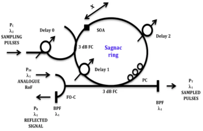
Figure 2 depicts the proposed fibre-optic circuit design of the o-Sampler. The circuit uses two 3-dB fibre-couplers (FC) and three optical delay lines. The “Delay 0” is used to perform the temporal alignment between the analogue and the sampling pulses (see Figures 7 and 8). Each single analogue cycle can be adjusted to symmetrically encompass 5 sampling pulses (as is shown in Figure 8). The perimeter of the Sagnac fibre-ring must be kept constant and equal of an integer number of periods of the analogue signal. Therefore, the “Delay 1” and “Delay 2” allows fine and independent adjustments of the asymmetric placement “x” of the SOA in reference of the midpoint of the ring. In other words, the “Delay 1” and “Delay 2” allow independent adjustment of temporal coincidence of the CW and CCW analogue signal when they propagate along the SOA excited by the sampling pulses. The polarisation controller PC allows initial adjustment of the ring to be 100% reflective when the control power (sampling pulses) is turned-off, i.e. PC = 0 mW. The sampled pulses are collected from the transmission arm (PT) of the interferometer. The band-pass filters BPF centred in λ1 reduce the ASE noise from the SOA and can block the sampling pulses light (λ2). As a result, the transmitted PT and the reflected PR powers and waveforms are both measured at the same wavelength λ1 of the input analogue signal PIN.
The power of the transmitted (PT) sampled pulses of an ideal Sagnac interferometer is given by the transfer function (1) [7,26].
PT = ½ PIN [1- cos(2γLSOAPC)] (1)
In (1), Δφ = 2γLSOAPC means the XPM-generated differential phase-shift between the CW and CCW [7]
analogue signals, respectively. The Δφ phase-shift depends on the optical nonlinear strength γ and the length LSOA of the SOA inserted in the ring, and the peak power PC of the launched sampling pulses. The SOA inserted in the Sagnac ring is an active element and the output signal will experiment an optical gain, i.e. PT > PIN.
In the absence of sampling pulses, Δφ = 0 rad, the SLALOM acts as a perfect mirror (after a proper adjustment of the PC) for the analogue signal that is totally reflected back, i.e. PT = 0 mW according (1). The sampling pulses are launched by means of a fibre-coupler (3 dB-FC) and propagate along the SOA thus imprinting a phase-shift in a very small portion of the analogue signal waveform. Such phase-shift occurs due to the XPM effect that takes place into the SOA. Since the SOA is asymmetrically placed in the Sagnac ring, the Δφ phase-shift is imprinted in slightly different parts of the CW and CCW analogue waveforms. This change in phase means that during the timewidth of the sampling pulses the Sagnac loop turn to be transmitting. However, the SOA response should not be necessarily fast. As is better explained in the next section, by adjusting the “Delay 1” (and also the “Delay 2”) at few picoseconds, say 10-20 ps, it opens a switching window and the switching efficiency may be controlled at some extent.
Fig. 2. The fibre-optic circuit design of the o-Sampler.
IV. MODELLING AND SIMULATION OF THE O-SAMPLER
The physical model solves the nonlinear Schrödinger equation (NLSE) taking into account the SPM and XPM effects in the bulk and isotropic SOA as an active (amplifier) nonlinear waveguide. The model assumes a SOA with low feedback and uses the Transmission Line Model (TLM) to compute the differential nonlinear phase-shift induced by a change in carrier density in the semiconductor. As a result, the switching driven by the sampling pulses is due the XPM effect occurring into the SOA. Table I shows the o-Sampler circuit parameters as used in the computer simulations.
It should be observed that the real peak power PC of the sampling pulses is the half of the launched into the circuit (see Figure 2). The reason is because a conventional 3 dB fibre-optic coupler is used instead of a WDM-coupler to launch the control power into the SOA.
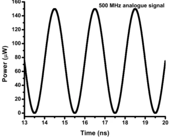
Figure 3 shows the plot of the sinusoidal analogue signal PIN with 150 µW amplitude at carrier frequency of 500 MHz or 2-ns period that is launched into the o-Sampler circuit. The PIN is assumed to be a RoF signal not carrying modulation on the RF carrier. The aim here is only to show the possibility of sampling with the circuit design shown in Figure 2.
Fig. 3. The analogue RoF sinusoidal waveform at 500 MHz frequency as to be the input signal into the o-Sampler circuit.
Figure 4 shows the plot of the sampling pulses at PC = 80 µW peak power at 2.5 GHz repetition rate and 40-ps timewidth.
Before the simulations of the optical sampling itself, the PC (or the initial relative optical phase between CW and CCW) is adjusted to set the Sagnac ring to be 100% reflective without sampling pulses. Figure 5 shows the plot of the reflected (R) and transmitted (T) analogue signal for PC = 0 mW. The
reflected analogue signal is amplified by 20.8 dB thus reaching 18 mW.
Fig. 4. The control signal at 2.5 GHz & 40-ps as the sampling pulses launched into the o-Sampler circuit.
Fig. 5. The reflected (R) and transmitted (T) analogue signal from the o-Sampler for PC = 0 mW after polarisation adjustment.
Hereafter, the delay adjustments were set to be Delay 0 = 300-ps, Delay 1 = 2.000-ns, Delay 2 = 6.000-ns and the sampling pulses were turned-on at PC = 15 mW (or effectively at 7.5 mW). It must be observed that Delay 1 + Delay 2 = 8.000-ns, i.e. 8-ns/2-ns = 4 analogue cycles fitted along the Sagnac ring perimeter. Therefore, the sampling pulses could imprint phase-shifts in the same temporal position of the analogue CW and CCW signals. As a result, almost none transmitted sampled pulses were achieved, i.e. the central sampled pulse at < 0.2 mW peak power with the envelope buried in some noise were calculated.
By slightly detuning the optical delays as to be Delay #1, i.e. Delay 1 = 1.995-ns and Delay 2 = 6.005-ns, the switching efficiency dramatically increases and the central sampled pulse reaches 2 mW peak power, an increase of > 10 dB when compared with previous setting. A further slightly detuning as to be now Delay #2, i.e. Delay 1 = 1.990-ns and Delay 2 = 6.010-ns, enables an even larger switching efficiency now reaching 4.5 mW peak power, i.e. an increase of 13.5 dB.
Figure 6 comparatively shows the central sampled pulses in a higher temporal resolution for both Delay #1 and Delay #2 under PC = 15 mW, reaching 2.0 mW and 4.5 mW peak power, respectively. Both pulses are also compressed to reach 20-ps timewidth, i.e. the half in comparison with the sampling pulses. A small temporal shift of ~ 8-ps between the pulses is observed. However, the ratio of 8-ps/2-ns = 0.4% is in principle regarded to be negligible when compared with the period of the analogue waveform.
Fig. 6. The central sampled pulses for the Delay #1 and Delay #2 setting at PC = 15 mW.
Figure 7 comparatively shows the transmitted “T” sampled pulses enveloped by the analogue signal waveform that coincides in time with the “sliced” reflected “R” signal.
Fig. 7. The transmitted sampled (T) pulses and the “sliced” analogue reflected (R) signal at PC = 15 mW.
From few µW to few mW peak power range of sampling control pulses, the calculated sampled pulses were unstable. This is because the SOA is far to exhibits the gain saturation and the nonlinearity strength vary from pulse-to-pulse. However, starting from PC = 15 mW, stable sampled pulses could be calculated to exit the o-Sampler when the PC is increased. This is because at 15 mW, a steady state is already reached after the partial carrier depletion in SOA due the
relatively high power of the sampling pulses. Figure 7 also shows that the dip of the “sliced” reflected signal has not the same value of the amplitude of the corresponding sampled pulses. The carrier depletion in the semiconductor under light pump is a very fast process whereas the generation of the sampled pulses follows the switching window after setting the Delays #1 and #2. Therefore the energy that is switched from the each “slice” of the reflected signal is essentially the same of that is contained in the corresponding sampled pulse. When the switching window closes, the sampled pulse is already shaped and the SOA gain begins to slowly recovering until the arrival of the next sampling pulse in a steady-state regime.
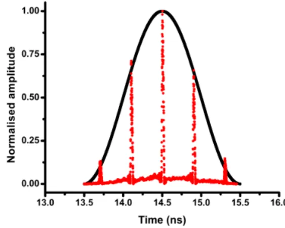
Figure 8 shows the normalised plots of the five sampled pulses that are contained and enveloped by a single cycle of the analogue signal using PC = 15 mW. It demonstrates the reasonably linearity of the proposed o-Sampler to carry out the sampling process.
Fig. 8. The normalised plots of the sampled pulses enveloped by the analogue signal at PC = 15 mW.
The optical components required to set-up the circuit shown in Figure 2 are similar of those used in an optical sampler based on the nonlinear polarisation rotation [15,16]. In the present fibre-based scheme, none polarisation-discriminator device is needed and only a single PC is required to set PT = 0 mW for PC = 0 mW. Another interesting feature of the present o-Sampler is the observation that the sampled pulses are compressed from 40-ps of the sampling pulses to the 20-ps timewidth. The temporal compression of pulses launched in Sagnac rings is expected because when a sampling pulse starts and ends (low pump power), the differential phase-shift is very low and then PT ≅ 0 mW. When the pump power increases (and decreases), the increase (decrease) in the transmitted power is not linear thus leading the compression of sampled pulses. However, such compressed pulses are useful for the next sub-module of the o-DRoF-T, i.e. the 3’ and 3’’ o-Interleavers [20]. The reduced timewidth allows more densely optical multiplexing in time and then an increase in the serialised bit resolution of the o-DRoF-T [20].
The SOAs itself are relatively complex devices to be designed. It should be treated not only as an optical amplifier
but also as a nonlinear waveguide where analogue signal and sampling pulses are propagating and interacting with each other. The dynamics of operation are not trivial. Besides those parameters here adjusted, many others can or should be simultaneously taken into account: wavelengths of the analogue signal and sampling pulses, the use of a continuous wave holding beam [27] to obtain gain saturation and faster nonlinearities, semiconductor structure and length of the SOA, etc.
V. CONCLUSIONS
To the best of our knowledge, neither experimental nor commercially available o-DRoF links or networks have been reported as they are still under R&D stage. This paper proposes a transmitter module comprising at least five optical sub-modules for use in an o-DRoF link. The o-DRoF-T is potentially stable in hundreds of GSa/s due the use of a mode-locked laser as the clock signal and is able to deals with RoF (optical) signal, i.e. none optoelectronic conversion is needed. It was proposed, designed and simulated here only the o-Sampler sub-module under control pulses launched in a single direction. The circuit operate at 1550 nm wavelength window. It provides some useful characteristics: compactness, prone to optical integration, requirement of few mW optical power for sampling pulses, polarisation independence, linearity and amplified output. D. Cotter et al also describe the realization of a SLALOM circuit on a single 1x2 mm InP semiconductor chip [22] that supports the possibility of optical integration of the proposed o-DRoF transmitter.
In this paper, the simulations were constrained to only 2.5 GHz & 40-ps RZ input sampling pulses mainly to demonstrate the proof-of-principle of the proposed real-time o-Sampler able to produce 2.5 GS/s sampled pulses. However, SOAs operating at 80 Gb/s are already commercially available [25]. Furthermore, SOAs incorporated in fibre circuits in R&D stage able to operate up to 160 Gb/s [28] and 320 Gb/s [29] were already reported.
Simulations and experiments of the o-Sampler operating at higher sampling pulse rate with shorter timewidth, other independents sub-modules of the proposed o-DRoF transmitter as well such transmitter as a whole are currently planned or in progress and will be presented in a near future.
ACKNOWLEDGMENT
Ricardo M. Ribeiro thanks the team at Département d’Optique of Telecom Bretagne and the CapilRTM platform for hosting his Post-Doctoral study during which the present work was carried out. The authors also thank INCT-Fotonicom/CNPq.
REFERENCES
[1] R. C. Williamson and R. D. Esman, RF Photonics, IEEE Journal of Lightwave Technology, Vol. 26, No. 9, 2008, pp. 1145-1151.
[2] A. Nirmalathas et al, Digitized Radio-Over-Fiber Technologies for Converged Optical Wireless Access Network, IEEE Journal of Lightwave Technology, Vol. 28, No. 16, 2010, pp. 2366 –2375. [3] S. R. Abdollahi, H. S. Al-Raweshidy and R. Nilavalan, Fully-Photonic
Analogue-to-Digital Conversion Technique for Super-Broadband Digitized-Radio over Fibre Link, 16th European Conference on Networks
and Optical Communications, Newcastle, UK, July 20-22, 2011, pp. 72-75.
[4] S. R. Abdollahi et al, Digital Radio over Fibre for Future Broadband Wireless Access Network Solution, 6th International Conference on
Wireless and Mobile Communication, Valencia, Spain, September 20-25, 2010.
[5] S. R. Abdollahi et al, Non-Uniform Wavelength Allocation in All-Photonic Digitized-Radio over Fibre Access Network, 14th International
Symposium on Wireless Personal Multimedia Communications, Brest, France, October, 2011.
[6] A. Viglienzoni and H. Al-Raweshidy, Net! Works - Next Generation Network: Wireless-Optics Technology, European Technology Platform, White Paper, June 06, 2011.
[7] Y. Miyoshi et al, All-Optical Analog-to-Digital Conversion Using Split-and-Delay Technique, IEEE Journal of Lightwave Technology, Vol. 25, No. 6, 2007, pp. 1339-1347.
[8] R. M. Ribeiro, F. Lucarz and B. Fracasso, A Thresholder for All-Optical Digitising Radio-over-Fibre Transceivers, 17th Conference on Optical
Network Design & Modeling (ONDM 2013), Brest, France, April 16-19, 2013, pp. 160-165.
[9] K-I. Kitayama et al, Optical Signal Processing Device for A/D Converter Including Optical Encoders with Nonlinear Loop Mirrors, US Patent 7,423,564 B2, September 9, 2008.
[10] B. P. Nelson and N. J. Doran, Optical Sampling Oscilloscope Using Nonlinear Fibre Loop Mirror, Electronics Letters, Vol. 27, No. 3, 1991, pp. 204-205.
[11] C. H. Kwok et al, All-Optical Sampling System Using Nonlinear Optical Loop Mirror with Soliton Self-Frequency Shifted Control Pulses, Pacific Rim Conference on Lasers and Electro-Optics (CLEO/Pacific Rim 2005), paper CThC3-P6, 2005, pp. 1358-1359.
[12] M. Westlund, Fiber-Based All-Optical Sampling, Conference on Lasers and Electro-Optics (CLEO 2007), paper CThAA1, 2007, pp. 1-2. [13] A. Bogoni et al, New Optical Sampler Based on TOAD and Data
Postprocessing for Sub-Picosecond Pulse Resolution, IEEE Journal of Selected Topics in Quantum Electronics, Vol. 10, No. 1, 2004, pp. 186-191.
[14] T. Rampone et al, Conversion gain characterisation of optical radiofrequency signal mixing by all-optical sampling on SOA-MZI, Electronics Letters, Vol. 48, No. 24, 2012, pp. 1542-1543.
[15] S. Zhang et al, All-optical sampling based on nonlinear polarization rotation in Semiconductor Optical Amplifiers, Journal of Optoelectronics and Biomedical Materials, Vol. 1, No. 4, 2009, pp. 383-388.
[16] S. Zhang et al, All-optical sampling exploiting nonlinear polarization rotation in a single semiconductor optical amplifier, Optics Communications, Vol. 285, 2012, pp. 1001-1004.
[17] X. Hou et al, GSPS All-Optical ADC for Future Communication and Imaging, IEEE Military Communications Conference (MILCOM 2005), October 17-20, Vol.5, 2005, pp. 3310-3313.
[18] A. S. Dayoush et al, All-Optical ADC and its Applications in Future Communication Satellites, IEEE International Topical Meeting on Microwave Photonics (MWP’04), paper TC-1, 2004, pp. 182-185. [19] M. Currie, High-Performance Photonic Analog-to-Digital Converter and
Low-Noise Mode-Locked Fiber Laser, U.S. Navy, Final Report, NRL/MR/5650--03-8679, May 26, 2003.
[20] R. M. Ribeiro, F. Lucarz and B. Fracasso, Proposal and Design of an All-Optical Encoder for Digitising Radio-over-Fibre Transceivers, 18th
European Conference on Network & Optical Communications (NOC 2013), July 10-12, Graz, Austria, 2013 in press.
[21] G. Huang et al, All-Optical OOK to 16-QAM Modulation Format Conversion Employing Nonlinear Optical Loop Mirror, IEEE Journal of Lightwave Technology, Vol. 30, No. 9, 2012, 1342-1350.
[22] D. Cotter et al, Nonlinear Optics for High-Speed Digital Information Processing, Science, Vol. 286, 1999, pp. 1523-1528.
[23] M. Eiselt, Optical Loop Mirror with Semiconductor Laser Amplifier, Electronics Letters, Vol. 28, No. 16, 1992, pp. 1505-1507.
[24] J. P. Sokoloff et al, A Terahertz Optical Asymmetric Demultiplexer (TOAD), IEEE Photonics Technology Letters, Vol. 5, No. 7, 1993, pp. 787-790.
[25] 1550 nm Nonlinear SOA from Amphotonix, www.kamelian.com. [26] G. P. Agrawal, Applications in Nonlinear Fiber Optics, Academic Press,
USA, 2001, pp. 125.
[27] R. J. Manning and D. A. O. Davies, Three-wavelength device for all-optical signal processing, Optics Letters, Vol. 19, No. 12, 1994, pp. 889-891.
[28] K. Szuki et al, Error-free demultiplexing of 160 Gbit/s pulse signal using optical loop mirror including semiconductor laser amplifier, Electronics Letters, Vol. 30, No. 18, 1994, pp. 1501-1503.
[29] Y. Liu et al, Error-Free 320-Gb/s All-Optical Wavelength Conversion Using a Single Semiconductor Optical Amplifier, IEEE Journal of Lightwave Technology, Vol. 25, No. 1, 2007, pp. 103-108.
![Figure 1 depicts a flowchart of the basic transmitter module architecture of an o-DRoF link [7,8,19,20] able to digitise RoF signals](https://thumb-eu.123doks.com/thumbv2/123doknet/12148439.311607/3.892.476.834.292.596/figure-depicts-flowchart-transmitter-module-architecture-digitise-signals.webp)