Strained Silicon on Wafer Level by Wafer Bonding: Materials Processing, Strain Measurements and Strain Relaxation
M. Reichea, O. Moutanabbira, C. Himcinschia&, S. Christiansena§, W. Erfurth a, U. Göselea, S. Mantlb, D. Bucab, Q.T. Zhaob,R. Looc, D. Nguyenc, F. Musterd, and M.
Petzoldd
a Max Planck Institut of Microstructure Physics, Halle, Germany
b Institute of Bio- and Nanosystems, Research Centre Juelich, Juelich, Germany c IMEC, Leuven, Belgium
d Fraunhofer Institute for Mechanics of Materials, Halle, Germany
Different methods to introduce strain in thin silicon device layers are presented. Uniaxial strain is introduced in CMOS devices by process-induced stressors allowing the local generation of tensile or compressive strain in the channel region of MOSFETs. Biaxial strain is introduced by growing thin silicon layer on SiGe buffer and transferring it to an oxidized silicon substrates. The latter forms strained silicon on insulator (SSOI) wafer characterized by tensile strain only. Future CMOS device technologies require the combination of the global strain of SSOI substrates with local stressors to increase the device performance.
Introduction
Conventional MOSFETs have proven to be remarkably scalable to gate lengths of about 60 nm, which are compatible with the 130 nm high-performance CMOS technology node. Intrinsic device performance up to this node has increased by about 17 % per year, following an inverse gate-length (1/Lg) dependence commensurate with channel length
decrease. This performance increase has relied in part on the steady increase of channel carrier velocity due to gate-length scaling combined with innovations, such as retrograde channel doping and highly doped halos around very highly doped source and drain junctions. The intrinsic carrier transport properties in the channel material, however, have remained constant, i.e. those of the relaxed silicon lattice. From the 90 nm node onwards, additional innovations have been introduced to increase the channel carrier mobility, and hence allow continuation of velocity increase, by the imposition of strain in the silicon channel of otherwise conventional MOSFETs.
There are generally 2 different methods to introduce strain in the channel region: biaxial strain and uniaxial strain. Biaxial strain is also referred to as global strain and is introduced by epitaxial growth of Si and SiGe layers (substrate engineering). The strain is induced by the lattice mismatch between Si and SiGe. The advantages of SOI and biaxially strained silicon layers can be combined in a single substrate of strained silicon on insulator (SSOI). Its application is not limited by further scaling below 32 nm. On the
& Now at: Chemnitz University of Technology, Semiconductor Physics, Chemnitz,
Germany
other hand, uniaxial strain is generated by local structural elements near the channel region. Since these process modules that cause uniaxial strain are part of CMOS processes, uniaxial strain is also referred to as process-induced strain (PIS). Owing to the relative ease of integrating process-induced strain modules in conventional CMOS processes, strain enhanced scaling has relied on the development of new advanced methods of PIS. The application of local strain elements, however, is limited by further scaling to 32 nm and below making some of them ineffective or unfeasible. For instance, stressed nitride layers can furthermore not be applied by shortages of space (1, 2). Therefore new methods of strain generation in the transistor channel region are required. One possible option is the combination of global and local strain or, in other words, of biaxial and uniaxial strain.
Methods of Strain Generation
Local Strain (Process-Induced Strain)
Electron and hole mobilities respond to mechanical stresses in different ways. For MOSFETs with the [110] channel orientation on {001}-oriented silicon substrates, tensile strain along the [110] direction improves electron mobility but degrades hole mobility. Therefore, to improve both the electron mobility in n-channel MOSFETs (NMOS) and the hole mobility in p-channel MOSFETs (PMOS), the introduction of strain in the transistor channel needs to employ different approaches for NMOS and PMOS.
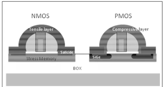
Advanced CMOS processes contain different process-induced stressors. These are mainly overlayers, embedded stressors, and stress memorization techniques (Fig. 1). Overlayers are typically stressed nitride layers deposited after salicidation of the source/drain and gate. Tensile overlayers are deposited over NMOS and compressive
Figure 1: Schematic representation of local stressors (process-induced stressors) in SOI CMOS. Tensile strain in NMOS is obtained by tensile overlayers and various stress memorization techniques. Compressive strain in PMOS is induced by compressive overlayers and embedded SiGe.
overlayers are deposited for PMOS. The strain in the channel region depends on the intrinsic stress of the layer, thickness of the layer, and device dimensions. Using tensile and compressive layers (dual stress liner, DSL) a significant hole mobility enhancement of 60% was achieved (3). Furthermore, important parameters of SOI CMOS devices, such as effective drive current enhancement, were proved in different 45 nm technologies. Stress memorization techniques (SMT) typically involve a nitride capping layer and an additional annealing step. They increase NMOS drive current and degrade the PMOS transistor.
Embedded SiGe layers (eSiGe) are widely used in PMOS transistors. Caused by the larger lattice constant of SiGe, compressive strain is induced in the channel. Currently this technique is improved by combining SiGe and SiC layers and mixtures of both (4, 5).
The integration of the different stressors into advanced CMOS technologies results in increasing device performance required by the ITRI road map (6). Typical effects of local stressors on the carrier mobility and the drive current (saturation drive current IDSAT and
linear drive current IDLIN) are summarized in table 1 for a SOI CMOS process (7). Similar
results of performance improvements have been also reported for CMOS processes on conventional bulk substrates (8, 9).
Table 1: Mobility, IDSAT, and IDLIN improvements for different stressor techniques.
Measurements on transistors prepared at the 65 nm technology node of a SOI CMOS process (7).
NMOS Electron Mobility IDSAT IDLIN
SMT 35% 10% 11%
Tensile Liner 27% 11% 2%
PMOS Hole Mobility IDSAT IDLIN
eSiGe 70% 23% 56%
Compressive Liner 90% 19% 39%
Global Strain
Global strain on wafer level is mostly induced by the epitaxial growth of Si1-x Gex and
Si layers. Because the lattice parameter of Si1-x Gex (0 ≤ x ≤ 1) alloys varies between
0.5431 nm for silicon (x = 0) and 0.5657 nm for germanium (x = 1) tensile strain is induced in a silicon layer epitaxially grown on top of the SiGe. The strain is generally biaxial. Furthermore, uniaxial strained layers are also obtained by mechanical straining.
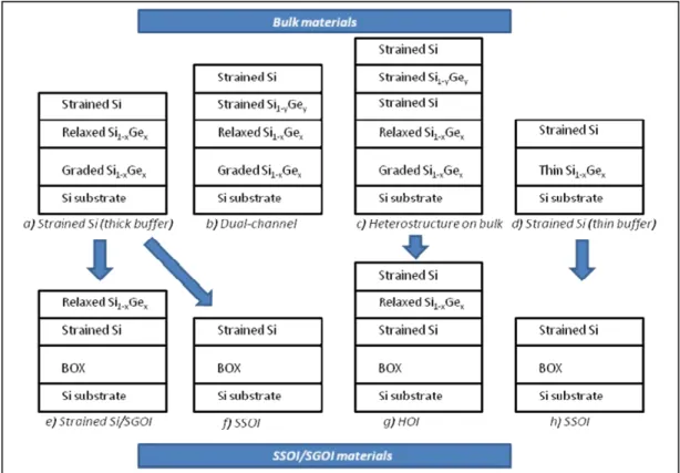
Biaxially strained layers. Figure 2 illustrates various heterostructure substrates that have been applied to biaxial strain and high-mobility channel materials. Epitaxially grown Si1-x Gex layers on Si bulk wafers are generally applied acting as substrate for a
strained silicon layer grown on top (bulk materials). In order to reduce the defect density in the strained silicon a relaxed Si1-x Gex buffer is required grown on a graded Si1-x Gex
layer (Fig. 2a). Because the Ge concentration x increases continuously by about 10 % per µm, the thickness of the graded buffer is several micrometers (Fig. 3a) (10, 11). An alternative is the relaxation of a thin pseudomorphic SiGe layer (< 500nm) induced by
hydrogen or helium implantation and subsequent annealing (Fig. 2d, 3b) (12, 13). Thinner SiGe buffer makes the process costs effective. Variations of the basic structure (Fig. 2a) have been also published including dual channel structures incorporating an additional strained Si1-y Gey layer with y > x (Fig. 2b) and heterostructures on bulk using
a second strained silicon layer (Fig. 2c) (9). Layer stacks of the types a, c, and d have been applied as virtual substrates for the preparation of SSOI and SGOI wafers. The
This paragraph represents the standard font and layout for individual paragraphs. A
Figure 2: Schematic illustration of various heterostructure substrates produced by epitaxial growth on bulk substrates (bulk materials) and by transfer of the strained layers to oxidized substrates (strained silicon on insulator (SSOI), strained Si/SiGe on insulator (SGOI)) (9, 17).
realization of SSOI wafers from bulk materials is a complex process combining wafer bonding, layer transfer, and etch-back methods. Processes using thick SiGe buffer layers were described, for instance, in references (14 – 16), while a process using thin buffer layers was published in ref. (17). The SSOI technologies provide a pathway to implementing mobility enhancement in partially or fully depleted devices, in ultrathin-body MOSFETs, or nonplanar (double-gate) MOSFETs. Mobility enhancement in SSOI was reported in (9) and (17) for the different SSOI configurations. Furthermore, long channel devices (Lg ≥ 1µm) show clearly improvements of the device characteristics. For
instance, drive current (IDSAT) improvements of 80% at the same source-to-drain leakage
(IOFF) has been measured. Improvements in the same order of magnitude were not
obtained for short channel devices. Here, an IDAST improvement of only 10 – 20% was
obtained up to now (17). The main reason was the interaction with process-induced stressors reducing the effect of the biaxial strain (18). This means that applications of SSOI wafers require modifications of existing CMOS processes. The combination of biaxially strained SSOI and optimized uniaxial stressors (dual-stress nitride capping layer and embedded SiGe) was already demonstrated resulting in IDSAT improvements of 27%
and 36% for n-channel MOSFETs and p-channel MOSFETs, respectively, in sub- 40 nm devices (19). In addition, the gate leakage current was also reduced by 30%. All investigations suggest that the combination of biaxially strained SSOI and uniaxial strain by process-induced stressors is the optimum way for future requirements (2, 9, 18, 19). Uniaxial strained layers: A concept to realize uniaxial strain on wafer level was published in ref. (20). Two wafers were bent over a cylinder thereby creating a curved or bowed wafer with a strained state induced. The bending direction was parallel to [110]. The curved wafers are brought into contact via direct wafer bonding and covalent bonds
a)
b)
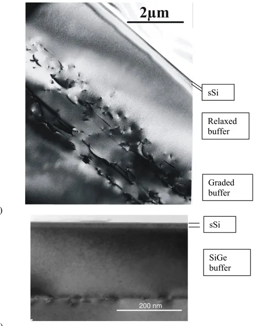
Figure 3: Typical XTEM images of the strained Si/SiGe bulk heterostructures used as virtual substrates for SSOI fabrication.
a) a relaxed Si0.83Ge0.17 layer (about 2 µm thick) is grown on top of a compositional
graded layer corresponding to the schema in Fig. 2a;
b) strained silicon layer on top of a pseudomorphically grown Si0.77Ge0.23 layer after
relaxation by He implantation and subsequent annealing (corresponding to schema in Fig. 2d). sSi Relaxed buffer Graded buffer sSi SiGe buffer
across the bonded interface form upon annealing in the bent state. By combining the process with hydrogen-induced layer splitting thin strained layers were transferred. The process can generally be used to realize strained layers of either tensile or compressive strain. The strain introduced by this technique is significantly lower as for biaxially strained layers. Depending on the radius of curvature strain values between about 0.08% and 0.04% were obtained for a radius of curvature ranging from 0,5 m up to 1 m.
Characterization of Strain
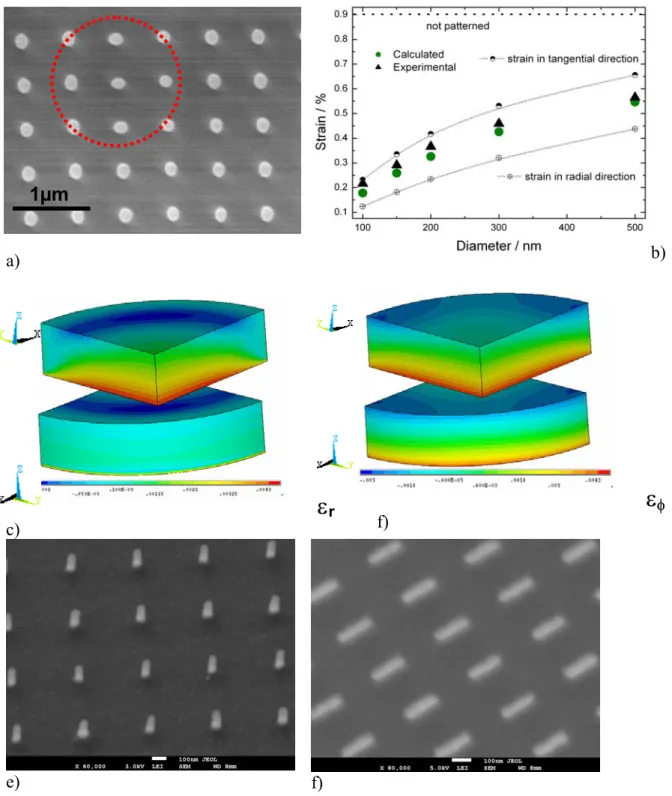
There is a large number of methods to measure the strain in thin layers but only a few are applied to strained silicon. For characterization of strain in non-patterned layers X-ray diffraction methods and UV- Raman spectroscopy are generally used. Especially UV- Raman spectroscopy is the method of choice because it is a non-destructive method, easy to handle, allows fast measurements, and can be applied in CMOS process lines. Because the penetration depth of the laser light mostly used for excitation (λ = 325nm) is about 10 nm in silicon, UV Raman spectroscopy is applicable also for very thin strained silicon layers required for fully depleted device fabrication. The application of the conventional UV-Raman technique, however, is limited to patterned device layers. For instance, Fig. 4a shows the SEM image of a patterned strained silicon layer on top of a SiGe buffer. Round strained silicon pillars having a diameter of 100nm were realized by electron beam lithography and dry etching. Using a µ-Raman setup and a He-Cd laser with λ = 325 nm, the diameter of the laser beam on the sample is about 1.5 µm. Since the dimension of the laser spot is larger than of the patterned pillars, a single Raman measurement contains contributions of more than one pillar and from the underlying SiGe buffer. The different positions of the Si-Si vibration modes in the strained silicon and SiGe allow the integral measurement only of a few pillars. The results show that patterning causes a distinct strain relaxation that is significantly increasing if the pillar diameter is reduced from 500 nm down to 100 nm (Fig. 4b). Numerical simulations of the strain relaxation are in agreement with the measured data. In addition, finite element simulation of the strain distribution in individual pillars were also carried out proving that the strain relaxes rather close to the free surfaces while remains concentrated at the interface between the strained silicon and the underlying SiGe buffer (21).
Analogous measurements on patterned strained silicon layers on an oxide (as for SSOI) cause that the strong Si-Si vibration mode of the silicon base wafer appears and the Si-Si vibration mode of the thin strained silicon structures cannot clearly be identified anymore. One possible solution to measure structures as shown in Figs. 4e, f is the reduction of the wavelength of the exciting laser. First measurements using a laser excitation at λ = 244 nm (frequency-doubled Ar ion laser) indicate that patterns having dimensions of 80 nm x 120 nm can be analyzed (22). The laser spot on the sample surface is about 500 nm and, using distances between individual structures in the same range, the measurement of single structures is possible.
Alternative techniques applicable to structures in strained silicon having feature sizes below 100 nm could be tip-enhanced (TERS) or surface-enhanced (SERS) Raman spectroscopy. Only first results exist up to now to their applicability for strained silicon on a SiGe buffer layer (23) and on SSOI (24). Besides Raman spectroscopy, also electron microscope methods were used either by analyzing the high-order Laue zone (HOLZ)
a) b)
c)
e) f)
Figure 4: SEM images of patterned round strained silicon pillars on a SiGe buffer (a). The dotted circle indicates the laser spot size. Comparison of strain values measured by µ-Raman spectroscopy (triangles) and calculated by finite element modeling for pillars having diameters ranging from 100 nm to 500 nm (b). Strain distribution obtained by finite element calculations within a round strained Si pillar with a diameter of 100 nm on the radial (c) and tangential (d) polar coordinates (21). SEM images of rectangular structures produced in a 20 nm thick strained silicon layer of a SSOI wafer. The dimensions of the structures are 50 nm x 100 nm (e) and 80 nm x 120 nm (f).
1µm
ε
rε
φlines using convergent-beam electron diffraction (25) or nanoscale holographic interferometry (26). Both techniques are destructive and applied up to now only to devices.
Conclusions
Wafer bonding and layer transfer in combination with hydrogen-induced layer splitting is an effective approach to realize SSOI substrates using different virtual substrates. The strain in the silicon layer is tensile. The combination of the global strain of SSOI with local (process-induced) stressors is most important to improve important parameters of n-channel and p-channel MOSFETs simultaneously in future high-performance device technologies. The scalability of some of the process-induced stressors, on the one hand, is limited. This requires new techniques for stress generation on device level. On the other hand, band structure modeling proved that strong confinement cancels out some of the band splitting and effective mass reduction offered by biaxial tensile strain in ultrathin SOI (26). Consequently, higher levels of strain are required in order to get a band splitting similar to that observed in bulk strained silicon.
Acknowledgments
We are thankful to S. Hopfe and R. Scholz for the sample preparation and XTEM investigation.This work was financially supported by the German Federal Ministry of Education and Research in the framework of the TeSiN project (contract no. V03110).
References
1. A. Oishi, O. Fujii, T. Yokoyama, K. Ota, T. Sanuki, H. Inokuma, K. Eda, T. Idaka, H. Miyajima, S. Iwasa, H. Yamasaki, K. Oouchi, K. Matsuo, H. Nagano, T. Komoda, Y. Okayama, T. Matsumoto, K. Fukasaki, T. Shimizu, K. Miyano, T. Suzuki, K. Yahashi, A. Horiuchi, Y. Takegawa, K. Saki, S. Mori, K. Ohno, I. Mizushima, M. Saito, M. Iwai, S. Yamada, N. Nagashima and F. Matsuoka,
IEDM Techn. Digest, p. 239 (2005).
2. A. Thean, in Silicon-on-Insulator Technology and Devices 13, G.K. Celler, S. Cristoloveanu, S.W. Bedell, F. Gamiz, B.-Y. Nguyen and Y. Omura, Editors, ECS
Transactions, 6(4), p. 287, The Electrochem. Society, Pennington, NJ (2007).
3. H.S. Yang, R. Malik, S. Narasima, Y. Li, R. Divakaruni, P. Agnello, S. Allen, A. Antreasyan, J.C. Arnhold, K. Bandy, M. Belyansky, A. Bonnoit, G. Bronner, V. Chan, X. Chen, Z. Chen, D. Chidambarro, A. Chou, W. Clark, S.W. Crowder, B. Engel, H. Harifuchi, S.F. Huang, R. Jagannathan, F.F. Jamin, Y. Kohyama, H. Kuroda, C.W. Lai, H.K. Lee, W-H. Lee, E.H. Lim, W. Lai, A. Mallikarjunan, K. Matsumoto, A. McKnight, J. Nayak, H.Y. Ng, S. Panda, R. Rengarajan, M. Steigerwalt, S. Subbanna, K. Subramanian, J. Sudijono, G. Sudo, S-P. Sun, B. Tessier, Y. Toyoshima, P. Tran, R. Wise, R. Wong, I.Y. Yang, C.H. Wann, L.T. Su, IEDM Techn. Digest, p. 1075 (2004).
4. Y.C. Yeo, Semicond. Sci. Technol. 22, S177 (2007).
5. M. Wiatr, Advanced SOI CMOS transistor technology for high performance microprocessors, MAR08 Meeting of the American Physical Society, Abstr., March 10-14, New Orleans.
6. International Technology Roadmap for Semiconductors, Update 2006.
7. M. Horstmann, A. Wei, T. Kammler, J. Höntschel, H. Bierstedt, T. Feudel, K. Frohberg, M. Gerhardt, A. Hellmich, K. Hempel, J. Hohage, P. Javorka, J. Klais, G. Koerner, M. Lenski, A. Neu, R. Otterbach, P. Press, C. Reichel, M. Trentsch, B. Trui, H. Salz, M. Schaller, H.-J. Engelmann, O. Herzog, H. Ruelke, P. Huebler, R. Stephan, D. Greenlaw, M. Raab, N. Kepler, H. Chen, D. Chidambarro, D. Fried, J. Holt, W. Lee, H. Nii, S. Panda, T. Sato, A. Waite, S. Luning, K. rim, D. Schepis, M. Khare, S.F. Huang, J. Pellerin, and L.T. Su, IEDM Techn. Digest, p. 243 (2005).
8. K. Mistry, M. Armstrong, C. Auth, S. Cea, T. Coan, T. Ghani, T. Hoffmann, A. Murthy, J. Sandford, R. Shaheed, K. Zawadzki, K. Zhang, S. Thompson, and M. Bohr, 2004 Symp. on VLSI Technology, Digest, p. 50 (2004).
9. D.A. Antoniadis, I. Aberg, C. Ni Chleirigh, O.M. Nayfeh, A. Khakifirooz, and J.L. Hoyt, IBM J. Res. & Dev. 50, 363 (2006)
10. P.M. Mooney, Mater. Sci. Eng. R 17, 105 (1996).
11. E.A. Fitzgerald, Y.-H. Xie, M.L. Green, D. Brasen, A.R. Kortan, J. Michel, Y.-J. Mii, and B.E. Weir, Appl. Phys. Lett. 59, 811 (1991).
12. S. Mantl, B. Holländer, R. Liedtke, S. Mesters, H.-J. Herzog, H. Kibbel, and T. Hackbarth, Nucl. Instrum. Meth. Phys. Res. B 147, 29 (1999).
13. S. Mantl, D. Buca, B. Holländer, St. Lenk, N. Hueging, M. Luysberg, R. Carius, R. Loo, M. Caymax, H. Schäfer, I. Radu, M. Reiche, S. Christiansen, and U. Gösele, in SiGe and Ge: Materials, Processing, and Devices, GD. Harame et al., Editors, ECS Transactions, 3(7), p. 1047, The Electrochem. Society, Pennington, NJ (2006).
14. K. Rim, K. Chan, L. Shi, D. Boyd, J. Ott, N. Klymko, F. Cardone, L. Tai, S. Koester, M. Cobb, D. Canaperi,, B. To, E. Duch, I. Babich, R. Carruthers, P. Saunders, G. Walker, Y. Zhang, M. Steen, and M. Ieong, IEDM Techn. Digest, p. 47 (2003).
15. T.A. Langdo, A. Lochtefeld, M.T. Currie, R. Hammond, V.K. Yang, J.A. Carlin, C.J. Vineis, G. Braithwaite, H. Badawi, M.T. Bulsara, and E.A. Fitzgerald, Proc.
IEEE SOI Conf. 2002, p. 211 (2002).
16. T.S. Drake, C. Ni Chleirigh, M.L. Lee, A.J. Pitera, E.A. Fitzgerald, D.A. Antoniadis, D.H. Anjum, J. Li, R. Hull, N. Klymko, and J.L. Hoyt, J. Electron.
Mater. 32, 972 (2003).
17. M. Reiche, C. Himcinschi, U. Gösele, S. Christiansen, S. Mantl, D. Buca, Q.T. Zhao, S. Feste, R. Loo, D. Nguyen, W. Buchholtz, A. Wie, M. Horstmann, D. Feijoo, and P. Storck, in Silicon-on-Insulator Technology and Devices 13, G.K. Celler, S. Cristoloveanu, S.W. Bedell, F. Gamiz, B.-Y. Nguyen and Y. Omura, Editors, ECS Transactions, 6(4), p. 339, The Electrochem. Society, Pennington, NJ (2007).
18. A. Wei, S. Dünkel, R. Boschke, T. Kammler, K. Hempel, J. Rinderknecht, M. Horstmann, I. Cayrefourcq, F. Metral, M. Kennard, and E. Guiot, in Advanced
gate stack, source/drain and channel engineering for Si-based CMOS 3, M.C.
Ötztürk et al. Editors, ECS Transactions, 6(1), p. 15, The Electrochem. Society, Pennington, NJ (2007).
19. A.V-Y. Thean, D. Zhang, V. Vartanian, V. Adams, J. Conner, M. Canonico, H. Desjardin, P. Grudowski, B. Gu, Z.-H. Shi, S. Murphy, G. Spencer, S. Filipiak, D. Goedeke, X-D. Wang, B. Goolsby, V. Dhandapani, L. Prabhu, S. Backer, L-B. La,
D. Burnett, T. White, B.-Y. Nguyen, B.E. white, S. Venkatesan, J. Mogab, I. Cayrefourcq, and C. Mazure, 2006 Symp. On VLSI Technology, Digest (2006). 20. C. Himcinschi, M. Reiche, R. Scholz, S. Christansen, and U. Gösele, Appl. Phys.
Lett. 90, 231909 (2007).
21. C. Himcinschi, R. Singh, I. Radu, A. Milenin, W. Erfurth, M. Reiche, U. Gösele, and S. Christiansen, Appl. Phys. Lett. 90, 021902 (2007).
22. O. Moutanabbir, M. Reiche, W. Erfurth, R. Scholz, and U. Gösele, Strain
relaxation in nanostructured ultra thin SOI, Paper # 08-122 presented at the 2008
IEEE Intern. SOI Conference, Oct. 6-9, 2008, Hudson River Valley, New York. 23. N. Hayazawa, M. Motohashi, Y. Saito, and S. Kawata, Appl. Phys. Lett. 86,
263114 (2005).
24. L. Zhu, J. Atesang, P. Dudek, M. Hecker, J. Rinderknecht, Y. Ritz, H. Geisler, U. Herr, R. Geer, and E. Zschech, Materials Science – Poland 25, 19 (2007).
25. P. Zhang, A.A. Istratov, E.R. Weber, C. Kisielowski, H. He, C. Nelson, and J.C.H. Spence, Appl. Phys. Lett. 89, 161907 (2006).
26. M. Hytch, F. Houdellier, F. Hüe, and E. Snoeck, Nature 453, 1085 (2008). 27. A. Khakifirooz, IEEE Electr. Dev. Lett. 27, 402 (2006)