UNIVERSITÉ DE MONTRÉAL
LOW-POWER HIGH DATA-RATE WIRELESS TRANSMITTER FOR
MEDICAL IMPLANTABLE DEVICES
ARASH MORADI
DÉPARTEMENT DE GÉNIE ÉLECTRIQUE ÉCOLE POLYTECHNIQUE DE MONTRÉAL
THÈSE PRÉSENTÉE EN VUE DE L’OBTENTION DU DIPLÔME DE PHILOSOPHIAE DOCTOR
(GÉNIE ÉLECTRIQUE) DÉCEMBER 2014
UNIVERSITÉ DE MONTRÉAL
ÉCOLE POLYTECHNIQUE DE MONTRÉAL
Cette thèse intitulée :
LOW-POWER HIGH DATA-RATE WIRELESS TRANSMITTER FOR
MEDICAL IMPLANTABLE DEVICES
présentée par : MORADI Arash
en vue de l’obtention du diplôme de : Philosophiae Doctor a été dûment acceptée par le jury d’examen constitué de :
M. AUDET Yves, Ph.D., président
M. SAWAN Mohamad, Ph.D., membre et directeur de recherche M. ZHU Guchuan, Ph.D., membre
DEDICATION
To my parents… for their never-ending love and support.
ACKNOWLEDGEMENT
I would like to thanks my supervisor, Prof. Mohamad Sawan, for his support and valuable comments during my Ph.D. studies at Polytechnique Montréal. His guidance and patience smoothed the path and made it possible for me to develop this thesis. I am also grateful of the jury members for generously accepting to evaluate my thesis.
My appreciation also goes to all my colleagues and friends in Polystim research group including but not limited to Faycal Mounaim, Omar Al-Terkawi, Amine Miled and Saeid Hashemi for their valuable fellowship in my journey. Likewise, I would like to thank our technicians, Réjean Lepage, Laurent Mouden and Jean Bouchard for their constant helps and supports that backed me to demonstrate my ideas as well as Marie-Yannick Laplante for her kind helps in the administrative level.
I am dedicating my thesis to my parents for their endless love and support along the way and I am thankful of my siblings, Simindokht, Amir and Sima, for their non-stop encouragement towards higher achievements. At last but not the least, I would like to thank my friends, primarily Mahsa Golkar for her inspiring and caring attitude as well as Kian Jalaleddini, Mina Ranjbaran and Omidreza Ghasemi, who kept their amiable company with me in the ups and downs during my stay in Montréal and
RÉSUMÉ
Les émetteurs-récepteurs radiofréquences (RF) sont les circuits de communication les plus communs pour établir des interfaces home-machine dédiées aux dispositifs médicaux implantables. Par exemple, la surveillance continue de paramètres de santé des patients souffrant d'épilepsie nécessite un étage de communication sans-fil capable de garantir un transfert de données rapide, en temps réel, à faible puissance tout en étant implémenté dans un faible volume. La consommation de puissance des dispositifs implantables implique une durée de vie limitée de la batterie qui nécessite alors une chirurgie pour son remplacement, a moins qu’une technique de transfert de puissance sans-fil soit utilisée pour recharger la batterie ou alimenter l’implant a travers les tissus humains.
Dans ce projet, nous avons conçu, implémenté et testé un émetteur RF à faible puissance et haut-débit de données opérant à 902-928 MHz de la bande fréquentielle industrielle-scientifique-médicale (ISM) d’Amérique du Nord. Cet émetteur fait partie d'un système de communication bidirectionnel dédié à l’interface sans-fil des dispositifs électroniques implantables et mettables et bénéficie d’une nouvelle approche de modulation par déplacement de fréquence (FSK). Les différentes étapes de conception et d’implémentation de l'architecture proposée pour l'émetteur sont discutées et analysées dans cette thèse. Les blocs de circuits sont réalisés suivant les équations dérivées de la modulation FSK proposée et qui mènera à l'amélioration du débit de données et de la consommation d'énergie. Chaque bloc est implémenté de manière à ce que la consommation d'énergie et la surface de silicium nécessaires soient réduites. L’étage de modulation et le circuit mélangeur ne nécessitent aucun courant continu grâce à leur structure passive.
Parmi les circuits originaux, un oscillateur en quadrature contrôlé-en-tension (QVCO) de faible puissance est réalisé pour générer des signaux différentiels en quadrature, rail-à-rail avec deux gammes de fréquences principales de 0.3 à 11.5 MHz et de 3 à 40 MHz. L'étage de sortie énergivore est également amélioré et optimisé pour atteindre une efficacité de puissance de ~ 37%. L'émetteur proposé a été implémenté et fabriqué à la suite de simulations post-layout approfondies. Les résultats de simulations et de mesure sont discutés et comparés avec ceux des émetteurs modernes démontrant ainsi la contribution de ce travail dans ce domaine de recherche
très populaire. Le facteur-de-mérite (FOM) a été amélioré impliquant essentiellement l'augmentation du débit de données et la réduction de la consommation d'énergie du circuit. L'émetteur est implémenté en utilisant une technologie CMOS de 130 nm alimentée par une tension 1.2 V. Avec 1.4 mA de consommation de courant, un débit de données de 8 Mb/s a été mesuré résultant en une consommation d'énergie de 0.21 nJ/b. L'émetteur fabriqué occupe une surface active de silicium inférieure à 0.25 mm2.
ABSTRACT
Wireless radio frequency (RF) transceivers are the most common communication front-ends used to realize the human-machine interfaces of medical devices. Continuous monitoring of body behaviour of patients suffering from Epilepsy, for example, requires a wireless communication front-end capable of maintaining a fast, real-time and low-power data communication while implemented in small size. Power budget limitation of the implantable and wearable medical devices obliges engineers to replace or recharge the battery cell through frequent medial surgeries or other power transfer techniques.
In this project, a low-power and high data-rate RF transmitter (Tx) operating at North-American Industrial-Scientific-Medical (ISM) frequency band (902-928 MHz) is designed, implemented and tested. This transmitter is a part of a bi-directional transceiver dedicated to the wireless interface of implantable and wearable medical devices and benefits from a new efficient Frequency-Shift Keying (FSK) modulation scheme. Different design and implementation stages of the proposed transmitter architecture are discussed and analyzed in this thesis. The building blocks are realized according to the equations derived from the proposed FSK modulation, which results in improvement in data-rate and power consumption. Each block is implemented such that the power consumption and needed chip area are lowered while the modulation block and the mixer circuit require no DC current due to their passive structure.
Among the original blocks, a low-power quadrature voltage-controlled oscillator (QVCO) is achieved to provide differential quadrature rail-to-rail signals with two main frequency ranges of 0.3-11.5 MHz and 3-40 MHz. The power-hungry output stage is also improved and optimized to achieve power efficiency of ~37%. The proposed transmitter was implemented and fabricated following deep characterisation by post-layout simulation. Both simulation and measurement results are discussed and compared with state-of-the-art transmitters showing the contribution of this work in this very popular research field. The Figure-Of-Merit (FOM) was improved, meaning mainly increasing the data-rate and lowering the power consumption of the circuit. The transmitter is implemented using 130 nm CMOS technology with 1.2 V supply voltage. A data-rate of 8 Mb/s was measured while consuming 1.4 mA and resulting in energy consumption of 0.21 nJ/b. The fabricated transmitter has small active silicon area of less than 0.25 mm2.
TABLE OF CONTENTS
DEDICATION …… ... III ACKNOWLEDGEMENT ... IV RÉSUMÉ …. ……… ... V ABSTRACT ………. ...VII TABLE OF CONTENTS ... VIII LIST OF TABLES ... XI LIST OF FIGURES ...XII LIST OF ACRONYMS AND ABBREVIATIONS ... XVI LIST OF APPENDICES ... XVIII
CHAPTER 1 INTRODUCTION ... 1
1.1 RF transceivers in medical applications ... 1
1.1.1 Modulation: FSK vs. OOK ... 3
1.1.2 General RF Transmitter Architectures ... 5
1.2 Motivation ... 8
1.3 Research objectives and contributions ... 9
1.4 Thesis outline ... 11
CHAPTER 2 LOW-POWER ISM-BAND RF TRANSMITTERS: A REVIEW ... 13
2.1 RF transmitters in medical applications ... 13
2.2 Case studies of low-power 915 MHz transmitters ... 14
2.3 Summary ... 25
3.1 Target ISM-band transmitter ... 26
3.2 Proposed FSK modulation scheme ... 27
3.3 Proposed Transmitter Architecture ... 29
3.3.1 Block Diagram ... 29
3.3.2 Alternative spots for applying the modulation ... 31
3.3.3 Sensitivity over variation in phase and amplitude ... 32
3.4 Summary ... 37
CHAPTER 4 CIRCUIT DESIGN AND IMPLEMENTATION ... 38
4.1 Differential Quadrature Voltage-Controlled Oscillator (QVCO) ... 38
4.1.1 QVCO’s Block Diagram ... 39
4.1.2 QVCO’s Circuit ... 40
4.1.3 QVCO’s Start-Up Circuit ... 42
4.2 Poly-Phase Filter (PPF) ... 44
4.3 Passive Mixer ... 47
4.4 Transmitter’s Output Stage ... 49
4.4.1 Output stage in the fabricated Tx ... 49
4.4.2 Modification and optimization of PA ... 51
4.5 Transmitter Layout and Packaging ... 56
4.6 Summary ... 58
CHAPTER 5 SIMULATION AND MEASUREMENT RESULTS... 60
5.1 Fabricated Tx chip: Test-setup and general considerations ... 60
5.2 QVCO: Simulation and measurement results ... 62
5.3 DC simulation and measurements of the fabricated Tx ... 70
5.5 Comparison and discussion ... 80
5.6 Summary ... 83
CHAPTER 6 CONCLUSION AND FUTURE WORK ... 84
6.1 Conclusion ... 84
6.2 Recommendations For Future Work ... 87
REFERENCES ……… ... 89
LIST OF TABLES
Table 2.1: Summary of selected off-the-shelf low-power integrated ISM-band (915 MHz)
transmitters ... 21
Table 4.1: Transistors sizing of the optimized PA ... 53
Table 4.2: Comparison of similar CMOS power amplifiers ... 55
Table 4.3: Port definition of the integrated circuit ... 57
Table 5.1: Parameters of the delay cells for generating the frequency range of 0.3-11.57 MHz .. 62
Table 5.2: Parameters of the delay cells for generating 3-40 MHz ... 64
LIST OF FIGURES
Figure 1.1: RF Transceivers used for human-machine wireless interface ... 2
Figure 1.2: Generation of FSK signal from baseband data ... 4
Figure 1.3: General direct-conversion transmitter architecture ... 6
Figure 1.4: Two-step up conversion transmitter architecture ... 7
Figure 1.5: Target FSK transmitter in the communication front-end ... 9
Figure 1.6: General architecture for RF transmitters and receivers ... 10
Figure 2.1: Continuous monitoring of freely-moving rats using implanted transmitter [38] ... 14
Figure 2.2: Trend in recent energy-efficient binary FSK 915 MHz transmitters ... 15
Figure 2.3: The frequency multiplication used in [13]: (a) A1-9 phases from the oscillator and (b) schematic of the edge-combiner to multiply the frequency by 9 ... 18
Figure 2.4: Simplified FSK-based Tx diagram reported in [20] ... 23
Figure 2.5: Simplified TX architecture in [14] ... 24
Figure 2.6: The digitally implemented modulator in [14] ... 24
Figure 3.1: FSK modulation principle ... 27
Figure 3.2: Conceptual diagram of the proposed FSK Modulation ... 29
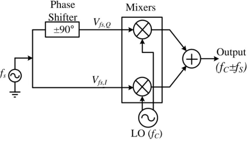
Figure 3.3: Simplified diagram of the proposed transmitter architecture ... 30
Figure 3.4: Proposed Transmitter Architecture ... 31
Figure 3.5: Choices for applying the modulation in the proposed transmitter architecture ... 32
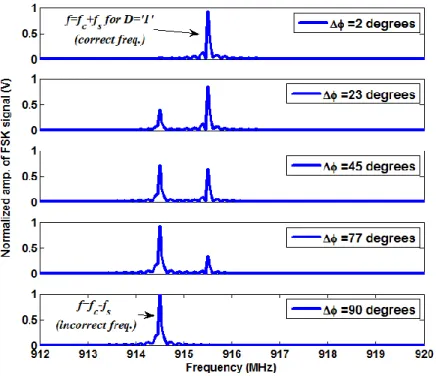
Figure 3.6: Output sensitivity over amplitude and phase discrepancy ... 33
Figure 3.7: Variation of VERR for ∆φ =1, 22, 45, 77 and 90 degrees when ∆a=0 ... 34
Figure 3.8: Frequency domain behavior of Vout(∆a,∆φ) for ∆φ =2, 23, 45, 77 and 90 degrees when ∆a =0 ... 35
Figure 3.9: Simplified block diagram of the test-bench for system-level verification of the
transmitter architecture in ADS software (See Appendix A) ... 36
Figure 3.10: Output generated FSK signal in ADS when data='1' and '0' ... 36
Figure 4.1: Block diagram of the 2-stage tunable quadrature oscillator including 2 delay cells and start-up ... 39
Figure 4.2: Proposed 2-stage quadrature voltage-controlled oscillator ... 40
Figure 4.3: Time-domain behaviour of I and Q signals showing the sequence of events in one period of T ... 41
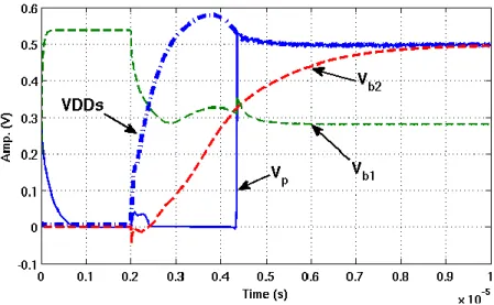
Figure 4.4: Start-up circuit: a) Schematic, and b) Transient behavior of its nodes ... 43
Figure 4.5: Simulated time-domain behavior of the nodes in start-up circuit ... 43
Figure 4.6: 2-stage PPF: a) Schematic, b) Simualted quadrature signals with fs=500 kHz ... 45
Figure 4.7: One stage of PPF layout with interleaved-shaped resistors to minimize mismatch. Ra1…4 form Ra in Figure 4.6 ... 45
Figure 4.8: Image reduction in PPF: a) Inputs configuration with fs=500 kHz, b) Outputs of the first and second stages in frequency domain ... 46
Figure 4.9: Effect of mismatch and process variation on quadrature signals due to 100 iterations of Monte-Carlo simulation ... 47
Figure 4.10: Differential CMOS passive mixer ... 48
Figure 4.11: Simulated mixers' outputs ... 48
Figure 4.12: Block diagram of the integrated transmitter’s output stage including the 2-stage PA ... 50
Figure 4.13: Transmitter’s output stage (fabricated chip) ... 50
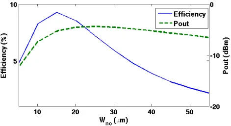
Figure 4.14: Efficiency and Pout vs. Wno, the width of Mno in output branch of Figure 4.13 ... 51
Figure 4.15: Modified and optimized power amplifier ... 53
Figure 4.17: Efficiency, Pout and total current vs. Vtune after optimization ... 54
Figure 4.18: Transmitter circuit (fabricated chip) ... 56
Figure 4.19: Transmitter layout (1.2×1.2 mm2) ... 57
Figure 4.20: Chip microphotography of the fabricated transmitter (1.2×1.2 mm2) ... 58
Figure 5.1: Simplified diagram of the setup used for testing the fabricated chip ... 61
Figure 5.2: The developed Printed Circuit Board (PCB) for measurement ... 61
Figure 5.3: Time-domain I and Q signals (related to frequency of 11.5 MHz when VDDOSC is 0.89 V) using the parameters of Table 5.1 ... 63
Figure 5.4: Frequency and current consumption of the proposed QVCO vs. VDDOSC related to parameters of Table 5.1 ... 63
Figure 5.5: A 2 MHz I/Q signal generated by the proposed QVCO with VDDOSC=0.45 V using paramters of Table 5.1 ... 64
Figure 5.6: Frequency and current of the oscillator vs. VDDOSC using parameters of Table 5.2 .. 65
Figure 5.7: 40 MHz I/Q signal generated by the proposed QVCO with VDDOSC=0.45 V using parameters of Table 5.2 ... 65
Figure 5.8: Variation in oscillation frequency for 100 iterations of Monte-Carlo simulation for a set of parameters in Table 5.1 when VDDOSC=0.5 V ... 66
Figure 5.9: Histogram of the oscillation frequencies due to 100 iterations of Monte-Carlo simulation ... 67
Figure 5.10: Produced signal of Vp in the start-up circuit due to 100 iterations of Monte-Carlo simulation ... 67
Figure 5.11: Produced delay due to signal of Vp in the start-up circuit due to 100 iterations of Monte-Carlo simulation ... 68
Figure 5.12: Histogram of the produced delays in the start-up circuit due to 100 iterations of Monte-Carlo simulation ... 68
Figure 5.14: Simulated and measured frequency and current consumption of the implemented
QVCO considering the external capacitive and resistive loads ... 70
Figure 5.15: Simulated and measured current consumption ... 71
Figure 5.16: Simulated FSK signal when data varies between '1' and '0' with 4 Mb/s rate related to the implemented transmitter using 130 nm technology ... 72
Figure 5.17: Simulated output FSK signal when data varies with 8, 10 and 20 Mb/s rates ... 73
Figure 5.18: Simulated output FSK signals when data='1' or '0' when Δf=0.5 MHz ... 74
Figure 5.19: Captured output FSK signals when Δf=4 MHz ... 74
Figure 5.20: Measured and simulated amplitude of the generated output signal (Pout) ... 75
Figure 5.21: Captured frequency variation vs. time for data-rate=100 kb/s and Δf=460 kHz ... 76
Figure 5.22: Captured frequency variation vs. time for data-rate=1 Mb/s and Δf=460 kHz ... 76
Figure 5.23: Captured frequency variation vs. time for data-rate=2 Mb/s and Δf=2 MHz ... 77
Figure 5.24: Captured frequency variation vs. time for data-rate=4 Mb/s and Δf=2 MHz ... 77
Figure 5.25: Demodulation properties of the captured 8 Mb/s FSK signal with frequency deviation of 4 MHz showing an average FSK error of 2.13% for 100 extracted bits ... 78
Figure 5.26: Demodulation properties of the captured 1 Mb/s FSK signal with frequency deviation of 1 MHz showing an average FSK error of 0.64% for 100 extracted bits ... 79
LIST OF ACRONYMS AND ABBREVIATIONS
ADC Analog to Digital Converter BFSK Binary Frequency-Shift-Keying BPF Band-Pass Filter
BSN Body Sensor Network
CMOS Complementary Metal-Oxide-Semiconductor DCO Digitally-Controlled Oscillator
IF Intermediate Frequency
ILFD Injection-Locked Frequency Divider ISM Industrial-Scientific-Medical
EEG Electroencephalography ESD Electrostatic Discharge
fNIRS Functional Near-Infrared Spectroscopy FOM Figure-Of-Merit FSK Frequency Shift-Keying GFSK Gaussian Frequency-Shift-Keying LC Inductor-Capacitor LO Local Oscillator MI Modulation Index OOK On-Off-Keying PA Power Amplifier
PPF Poly-Phase Filter PSK Phase Shift-Keying QFN Quad Flat No-lead
QVCO Quadrature Voltage-Controlled Oscillator
RF Radio Frequency
RFID Radio Frequency Identification RMS Root Mean Square
Rx Receiver
SNR Signal-To-Noise Ratio TRX Transceiver
Tx Transmitter
LIST OF APPENDICES
Appendix A Test-bench in ADS ………..……….……….…..….…94 Appendix B QVCO Layout …………..……….……….….….…95 Appendix C QVCO’s Start-Up Layout ……….….…..96
CHAPTER 1
INTRODUCTION
1.1 RF transceivers in medical applications
Medical applications of implantable and wearable body sensors keep short-range wireless communication as a challenging and hot research topic for monitoring and detection of various health parameters, such as temperature, pressure, oxygenation, seizures and other signs of diseases. For instance, the continuous monitoring of oxygen level of the blood for patients suffering from epilepsy may help locating, treating and even preventing the emerging of seizures. Even monitoring the behaviour of freely-moving animals, where free-running circuits are demanded, offers the chance to extract medical information in realistic conditions, thanks to wireless technologies. However, all requirements of a medical interface have to be considered and implementing such wireless communication interface remains challenging in many aspects.
Thanks to CMOS technology, the small size of the implemented front-ends helps to get rid of external bulky components. Among all challenges to realize the link between the implanted device and the external processing base station, the main challenge in addition to the size is in reducing the power consumption of the communication front-end for transferring information. Since the implanted devices have limitation over power storage, different circuits and systems design techniques have to be employed [1-4]. Radio Frequency (RF) transceivers, as the wireless communication front-end of body sensors, have the role of transmitting (Tx) and receiving (Rx) information (Figure 1.1) and usually they sink more than 90% of consumed power in emerging bio-devices. Data modulation is necessary to transmit the digital or analog data and to efficiently use the limited electrical bandwidth. Specific frequency ranges are allocated to be used as the electrical frequency bandwidth for the mentioned transceivers, mostly North-American Industrial-Scientific (ISM) frequency band (902-928 MHz) and European Medical-Implant-Communication-Service (MICS) frequency band (402-405 MHz). Consequently, the transceiver architecture and the employed modulation directly affect the performance of the target transmitter in terms of size, power consumption and data-rate.
Wireless sensor networks show their importance in communication for remote and inaccessible locations including inside the human body. Wireless transceivers are usually the most critical blocks in sensors in terms of power consumption. In addition to power consumption, the size, communication data-rate and, in total, designing high-efficiency wireless transceivers have been an interesting topic in circuit and system designs.
T° O2 RF Tx/Rx Body Sensors Short-Range Communicaiton Implantable/
Wearable Device External
Analysis
Figure 1.1: RF Transceivers used for human-machine wireless interface
In general, the transmitter power may be reduced to less than 1 mW in short-range communication application to relax the total current budget [5]. As an example, in the 400 MHz transmitter [6], the output power level is reduced to -59 dBm when the transmitter consumes less than 0.5 mW for transmitting each bit of data for a 1 m communication distance. As another example for monitoring freely-moving animals, a 900 MHz transmitter [7] consumes 1 mW to maintain the communication in ~2 m range. Power harvesting techniques may be used to power up the device, but, managing the collected power is a great challenge itself. The related reported front-end circuits in the literature and their performance are summarized and discussed in the following chapter.
In total, in addition to the current budget, the number of needed external components and maximum data-rate still remain challenging issues in implantable/wearable wireless communication devices. In practice, the medical sensor node is used to detect and monitor the target information from body using a number of channels, such as in electroencephalography (EEG) recordings. After the biomedical signal acquisition, the signal is digitized by an
analog-to-digital converter (ADC) with a specific sampling rate and reasonable precision. Finally, the extracted data can be processed (compressed for example) before the transmission starts with a high data-rate RF transmitter operating in range of few Mb/s [8].
The electrical bandwidth together with the signal-to-noise ratio, according to the well-known Shannon-Hartley theorem, defines the maximum communication channel capacity. Signal power level is usually defined according to the application and can be lowered in low-power applications to reduce energy consumption. In practice, the power level may be at least 30 to 40 dB higher than noise level and the attenuation caused by the working environment has to be considered. On the other hand, modulation is necessary to wisely use the limited electrical bandwidth and to physically transmit the digital or analog data. When the information signal is digital and the amplitude is varying according to the digital data, the Amplitude Shift-Keying (ASK) modulation, such as OOK, is used. Similarly, when the information is integrated into the frequency or phase, the modulation is called FSK and Phase Shift-Keying (PSK), respectively. In the following, characteristics of the FSK and OOK modulation schemes are briefly discussed and compared. Then, advantages and disadvantages of the common RF transmitter architectures, heterodyne and direct-conversion, are reviewed towards low-power implementation. In the next chapter, an overview on the architectures, behaviour, advantages and disadvantages of the low-power ISM-band transmitters is presented. The literature review is narrowed down to 915 MHz Binary FSK (BFSK) transmitters concluding that a high data-rate and low-power integrated design is mandatory for emerging medical devices.
1.1.1 Modulation: FSK vs. OOK
Proper choice of architecture results in how efficient the system can operate [9]. In order to have a low-power transceiver, the modulation scheme has to be as simple as possible. As reported in literature [10-19], the modulation schemes of FSK and OOK are widely used in transmitter (Tx) and receiver (Rx) building blocks, respectively, since they are phase independent and can be detected by non-coherent architectures. Implementing a data modulator with low-power consumption in wireless transceivers is of interest as the low-power budget is limited especially in implantable devices where long-life batteries are required.
In general, carrying information in the amplitude requires a highly linear power amplifier and the signal would be more susceptible to noise. In implantable and low-power consumption applications, where the level of signal is intentionally reduced, the information is more likely to be carried in the frequency. When the signal level is low, a linear power amplifier is needed in OOK modulation while FSK modulation has constant envelope with continuous phase and can be realized using non-linear power amplifiers [4, 20, 21]. In practice, the frequency content of the information is shifted up using a carrier frequency (fc) to reduce the effect of noise and disturbance from surrounding instrument and, hence, a Local Oscillator (LO) is necessary. In OOK, the biasing point of the transmitter circuit and the oscillator have to settle in less than a single bit period and this may limit the data-rate. Due to discontinuity in phase, the power spectrum of the binary PSK has larger side lobes than that of the binary FSK. As a result, FSK modulation is the best candidate in the implantable side while the OOK modulation is used in the external side. In FSK modulation, which is generally simpler than PSK in terms of detection, the center frequency is shifted to two close frequencies and this can be considered as sending the data of '1' and '0', as shown in Figure 1.2. The minimum bandwidth for FSK modulation is approximated as B=2(Δf+fd), where B is the channel bandwidth, Δf is the shifting frequency and
fd is the data-rate. In definition, Modulation Index (MI) for FSK modulation can be defined as the frequency deviation over the data-rate and the frequency deviation can be chosen due to bandwidth availability or data-rate requirement. Large modulation index of 2 in an FSK modulation, for example, can help relaxing the precision requirement [4] which means less deviation from the constellation points and, hence, smaller FSK error is expected.
t
Tx
t
Base-Band Signal BFSK Signal‘1’
‘0’
f
‘1’
‘0’
f
c+Δf
B
f
c-Δf
1.1.2 General RF Transmitter Architectures
Performance of any RF transmitter in terms of total power consumption and data-rate depends on its architecture and the employed modulation [22]. As reported in a survey in [9], which reviews the transceivers reported from 1997 to 2007 in IEEE Solid-State forums, Zero-IF architecture is a first choice for Rx path as well as Direct-Up Conversion for Tx path in most communication standards. Expensive and bulky heterodyne architectures with their high-power consumption are not acceptable for mentioned applications. Also, image-reject architectures suffering from first and secondary images need a high I/Q matching and even a two-step-up conversion still suffers from image problem. Low cost, high integration level, simplicity and having no image problem make the Zero-IF/Direct-Up Conversion architectures suitable for implantable transceivers.
A transceiver has both transmitter and receiver parts which may share one or more circuitries. RF modules are used for high speed data-transmission and they may be implemented with both analog and digital circuits. Since digital circuits may consume less power, in particular cases, and give advantage of scalability, it is preferable to bring the digital domain closer to the antenna which can be very challenging. Passive components may also be used to reduce the power consumption. Simplicity, data-rate and power dissipation as well as number of external components are the primary criteria in choosing transceiver architecture. Depending on the application and the required specifications, different architectures may be used to develop a transmitter. Practically, the goal is to modulate the data by varying one or more properties such that the transmission or reception would be beneficial in terms of speed and power consumption.
The RF transmitter performs modulation, up-conversion and power amplification. The two main transmitter architectures, Heterodyne and Direct-Conversion, are discussed in the following.
1.1.2.1 Direct-Conversion transmitters
To achieve a highly integrated and low-power consumption transceiver, direct-conversion method is used which can replace the heterodyne architecture. In this architecture, the baseband data is quadrature modulated while the I and Q signals are up-converted using a local oscillator
(ωc), as shown in Figure 1.3. Simplicity of this architecture makes suitable for implantable and low-power applications. Also, the image-rejection is no more a problem in the receiver side for direct down-conversion. In total, avoiding the problem of image-rejection and having less current consuming building blocks are two main benefits of this architecture [23]. Also, Direct-Up Conversion architecture needs a simple frequency plan for multi-standard designs [9].
PA
+
Cos (ωct) Matching Sin (ωct) TxData ModulatorI/Q Digital Domain
I
Q
Figure 1.3: General direct-conversion transmitter architecture
Notice that the baseband signals generated in the transmitter side are sufficiently strong and noise of mixers is not critical such as in receivers [22]. However, the leakage of PA output to the oscillator is still an issue since the output of the PA is a modulated waveform with high signal power and a spectrum centered around the LO frequency. Due to imperfection of shielding, injection pulling is inevitable and the noisy and amplified output of PA corrupts the spectrum of the oscillator. Moreover, phase and amplitude mismatch of I/Q signals in addition to DC offset and 1/f noise may lead to large error in constellation diagram and have to be minimized.
1.1.2.2 Two-Step transmitters (Heterodyne)
A heterodyne transmitter (Figure 1.4) is the reverse operation of a heterodyne receiver [1, 24]. Two-step up-conversion gives the advantage of having less severe issues with injection pulling as the baseband signal is up-converted in at least two steps using two oscillators (ω1 and ω2). As illustrated in Figure 1.4, the output frequency is far from the frequency of each oscillator. However, more filtering is needed and the band-pass filter (BPF) has to reject the unwanted sideband by large factor since the second up-converting mixer generates wanted and unwanted sidebands with equal magnitudes [22]. The necessity of off-chip passive components in filters
limits the integration aspect. Also, the additional oscillator circuit brings more complexity and power consumption to the architecture. In total, heterodyne architectures have a more reliable performance with a flexible frequency plan at the expense of being bulky and consuming more power than the direct-conversion based circuits.
PA
+
Cos (ω1t) Sin (ω1t) I BPF BPF Cos (ω2t) ω1 2ω1 ω ω1 2ω1 ω ω1-ω2 ω ω ω1+ω2 ω1+ω2 QFigure 1.4: Two-step up conversion transmitter architecture
Generation of RF signal, its modulation and driving it into an antenna are the basic functions of any RF transmitter [4, 22]. Direct-Up conversion architecture is chosen to avoid image-rejection problem. FSK modulation is also chosen to realize the transmitter side since OOK is strongly susceptible to interference and a linear power amplifier (PA) is required. In practice, two desired frequencies corresponding to data '1' and '0' are generated by the transmitter. The frequency deviation depends on the available channel bandwidth which is essential in narrow-band applications.
To sum up, the principles of the FSK modulation in comparison with OOK modulation were reviewed and it was conferred that the FSK modulation is more suitable and common for implantable transmitter section of a bidirectional transceiver while OOK modulation is more used for the receiver section. Then, the basic transmitter architectures, Direct-Conversion and Two-Step, were reviewed concluding that the Direct-Conversion architecture is more fit to integrated and low-power applications.
1.2 Motivation
Continuous monitoring and detection of health parameters of patients' body is practicable these days using new implantable and wearable biomedical sensors. Indeed, human-machine direct interaction can be minimized by using such wireless sensors and the patients do not need to be connected permanently (or for long period of time) to monitoring equipment. High energy-efficient circuits and systems design techniques are demanded to realize smart medical devices where low-power consumption, size and speed of communication are the priorities [25]. Different wireless sensor network (WSN) platforms may be used for health monitoring where wearable and implantable wireless circuits are needed. Such medical devices can have electrode-tissue interface or an implanted sensor and they may be used for detection of different body parameters such as temperature or drug delivery.
As depicted in Figure 1.1, Radio Frequency transceivers as the communication interface of wireless sensor networks (WSNs) are required in several biomedical applications such as monitoring brain activities for patients with brain diseases (Epilepsy). Such implanted devices have to consume very low power; otherwise, the battery cell of these devices has to be recharged through frequent medical surgeries. In general, the goal is to keep the implantable transmitter as simple and low-power as possible. Instead, the external receiver can be more complex.
The implemented transmitter in this thesis is dedicated to a target EEG-fNIRS brain monitoring sensor for patients suffering from Epilepsy, similar to [26]. In this research, the goal is to transfer the extracted information from blood to predict the seizure using up to 32 channels of EEG and 128 channels of fNIRS with 320 and 20 Hz needed sampling rate, respectively. A 16-bit analog-to-digital convertor (ADC) is also considered for digitization. The approximate required data-rate for real-time monitoring is then estimated by channels × sampling rate (Hz) × bits (ADC) resulting in about 500 kb/s of data-rate in the communication front-end. However, the data needs to be encoded and the necessary communication protocols have to be applied, which mean a throughput rate of 3 or 4 times higher in Mb/s range is necessary. One may use a novel encoding technique to lower the total needed power such as in [27], but the power-hungry analog front-end is usually the center of attention when low-power and high data-rate communication is of interest.
As a result, a much higher data-rate in range of few Mb/s is needed for real-time monitoring while the integrated front-end consumes as low power and small area as possible. In practice, a new modulation and architecture can be implemented to realize a low-power and high data-rate communication interface. Then, circuits of the composing building blocks in the designed architecture need to be carefully designed and implemented to minimize current consumption and area. Finally, the corresponding prototype has to be tested and verified according to the target requirements.
1.3 Research objectives and contributions
The RF integrated transmitter section of a power-efficient bidirectional communication front-end in the implantable side (Figure 1.5) is the target of this research. The transmitter section has to be carefully and separately investigated and implemented such that it is able to efficiently communicate with its external counterparts.
The goal of this research is to design and implement a binary Frequency-Shift-Keying (FSK) based integrated wireless transmitter section of the target transceiver, such as in Figure 1.6, operating at North American ISM frequency band with center frequency of 915 MHz. The main objectives for designing such RF transmitter are low-power consumption, high data-rate and small silicon area, as addressed in this thesis.
FSK Signal (OOK) (FSK) B o d y se n so r External 01 Wearable Rx Tx (FSK)Rx (OOK)Tx Short-range Communication Implantable/ 01 ….. Analysis
Figure 1.5: Target FSK transmitter in the communication front-end
In this project, a new FSK modulation scheme is introduced and developed using the basic modulation principles and the mathematics background. Reduction in total current consumption was the first advantage of the presented architecture and the corresponding block
diagram and initial implementation simulation results were published in a conference, CCECE 2011, titled as “A New FSK-based Transmitter Dedicated For Low-Power Wireless Medical
Transceivers” [28]. Freq. Synthesizer Wake-up Rx D ig it al D o m ai n Filter/ Demod. Filter/ Mod. Tx section Rx section PA LNA
Figure 1.6: General architecture for RF transmitters and receivers
The proposed transmitter architecture was implemented and optimized for high data-rate performance and the post-layout simulation results were published in a second conference paper, ICECS 2012, titled as “A 20 Mb/s 0.084 nJ/bit ISM-band Transmitter dedicated to medical
sensor networks” [29]. The performance of the presented transmitter and its characteristics were
also published in NEWCAS 2013, titled as “A 0.084 nJ/b FSK Transmitter And 4.8 μW OOK
Receiver For ISM-band Medical Sensor Networks” [30].
The proposed FSK modulation scheme and the corresponding transmitter architecture were further investigated and characterized. The alternatives for applying the modulation block as well as the sensitivity over phase and amplitude discrepancies were studied.
The circuits of the composing building blocks of the proposed transmitter architecture are adopted, designed and optimized towards low-power, high data-rate integrated transmitter. A new quadrature voltage controlled-oscillator (QVCO) was implemented to provide differential
rail-to-rail quadrature signals with tunable frequency from 300 kHz to 11.5 MHz with very small current consumption of 0.5 to 160 uA, respectively. This QVCO is in important building block in the proposed transmitter architecture to avoid additional external reference frequency. The interesting design point for this oscillator is the frequency of 2 MHz with current consumption of 5.5 uA. The results were published in the IET Electronics Letters, titled as “A New Differential
Rail-To-Rail Voltage-Controlled Quadrature Ring-Oscillator For Low-Power Implantable Transceivers”,
2014. Moreover, as an alternative frequency tuning range, the proposed QVCO oscillates at a frequency varying between 3 and 40 MHz with a current consumption of 3 to 117 uA, correspondingly. The related results are summarized and reported in chapter 5 of this thesis.
The layout of the designed transmitter was implemented for fabrication using the 130 nm CMOS technology to test and confirm the performance. Thanks to high frequency measurement setup, the experimental results were compared with state-of-the-art and similar related RF transmitters. The implemented transmitter prototype provided a data-rate of up to 8 Mb/s with 2.13% average FSK error while consuming 1.4 mA from a 1.2 V voltage supply and relatively small active silicon area of 0.25 mm2. The achieved measurement results were submitted to a journal paper, Analog Integrated Circuits and Signal Processing, titled as ”An Energy-Efficient
High Data-Rate 915 MHz FSK Wireless Transmitter for Medical Applications”, 2014. The
related simulation and measurement results as well as the developed test-setup are reported in chapter 5.
1.4 Thesis outline
In Chapter 2, the two widely-used data modulation schemes for low-power transceivers, FSK and On-Off-Keying (OOK), as well as two main transmitter architectures, Direct-Conversion and Two-Step, are reviewed and compared. A technical overview of low-power RF transceivers is presented. The transceivers are intended for the communication interface of medical implants where the size, power consumption and data-rate are the main challenges. The focus is narrowed down to integrated transmitters operating at ISM frequency band (915 MHz) and the design constraints and parameters as well as Figure-Of-Merit (FOM) are discussed.
In Chapter 3, a new efficient FSK modulation scheme is introduced and corresponding mathematical equations are presented towards realizing the block diagram of the target
transmitter. Characteristics and behaviour of the proposed modulation scheme, such as sensitivity, is then discussed. Finally, the proposed transmitter architecture is presented.
In Chapter 4, the building blocks in the proposed transmitter architecture are implemented in circuit- and layout-level. Alternative design and implementation choices for each block and their behaviour are briefly discussed. A novel low-power rail-to-rail differential QVCO, which can be tuned in different frequency ranges, is introduced and implemented. Special attention was paid to design the output stage of the transmitter, the Power Amplifier (PA), including its optimization. The final layout of the fabricated transmitter is also presented.
Post-layout simulation and measurement results of the integrated QVCO and the energy-efficient RF transmitter are presented in Chapter 5. Different parameters of the implemented QVCO and transmitter are investigated in simulation and measurement. The achieved performance of the proposed transmitter in this work is then compared with State-Of-The-Art showing the improvement in size, power consumption, data-rate and FOM.
Summary and conclusion of this dissertation are brought in Chapter 6, where the contributions of the overall work are outlined and benefits of this work are discussed. The possible future work is then discussed and a few related circuits are recommended to be designed and implemented.
In the Appendices, the related system-level test-bench and layouts of the implemented QVCO are shown.
CHAPTER 2
LOW-POWER ISM-BAND RF TRANSMITTERS: A REVIEW
2.1 RF transmitters in medical applications
As mentioned earlier, implantable wireless Microsystems for human bodies may be used to detect and transfer different information such as Oxygen level of the blood for treatment of different diseases [31]. Low-power CMOS RF transmitters have been always an interesting challenging research topic, such as the 915 MHz transmitter [32] published in 1996 with up to 160 kb/s and relatively large power consumption. The reported ISM-band low-power transmitters and their energy efficiencies are discussed in the following section. As a recent example of body implantable devices, a CMOS transceiver is presented in [33] for telemetry services. In [33], the transmitter side communicates at 400 MHz frequency range with a data-arte of 500 kb/s with an output power of -2.87 dBm while consuming 22 mW which is relatively high. The corresponding energy consumption is 44 nJ per transmitting bit. The power consumption has to be reduced by using less complex circuits or by improvement in data-rate which is directly affected by the architecture and the employed modulation. As another example, the Bluetooth module of [34] is produced in 2013 for communication with a data-rate of 186 kbps and energy efficiency of 13 nJ/b. Alternatively in [35], the battery-powered and wirelessly-powered RF body sensors are reported to be useful for monitoring of temperature and blood behaviour, for example, but the data-rate of the emerging methods is around 100 kb/s with a short period of operating time. In total, the goal is to come up with an energy-efficient communication front-end which consumes low power for transmitting each bit of data.
New medical experiments such as monitoring a given animal’s activity is feasible with light and tiny medical devices, such as battery-free RFID sensing tags on freely-behaving insect and small animals in [36] and [37]. Experiments on freely-moving rats are also very interesting where the micro-size integrated sensors are promising. For example, the telemetric system for recording EEG activity in freely-moving rat in [38] uses an implantable transmitter which communicates a sampling rate of 500 b/s with the external receiver via radio transmission over a short distance (less than 3m) similar to Figure 2.1. In this system the data-rate is reported 115.2
kb/s when 1.6 mA is drawn from two batteries of 1.55 V (~ 5 mW) for only 14 hours of measurements.
Figure 2.1: Continuous monitoring of freely-moving rats using implanted transmitter [38]
2.2 Case studies of low-power 915 MHz transmitters
In this section, the main FSK-based ISM-band transmitters are reviewed and studied. The state-of-the-art transmitters from literature, simulated and fabricated using CMOS technology, are summarized. The target range of current consumption is around 1 mA and the typical supply voltage is between 1.2 and 1.8 V depending on the used technology and the circuit design. Moreover, a few off-the-shelf transmitter chips are also reviewed to understand the level of performance in the market.
Comparing customized integrated RF transmitters is not an easy task due to the fact that each one is designed and optimized for a specific application with specific power level or frequency range and bandwidth. Consequently, similar designs with similar specifications have to be investigated to have a fair comparison.
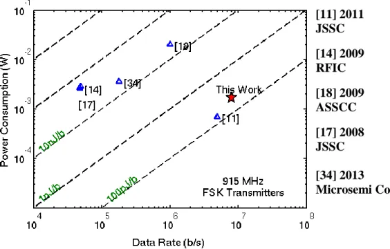
Figure 2.2 shows the power consumption of recent low-power 915 MHz binary FSK transmitters. Each of the mentioned transmitters in this graph is discussed in the following as well as other related transmitters. In this figure, the trend in power consumption and data-rate is summarized while the dashed lines shows the constant lines of consumed energy per transmitting bit. Other concerning parameters, such as size, simplicity and suitability for implantable medical devices, are also discussed in the following sections. Also, notice that the technical overview on the performance of the related ISM transmitters brought in this dissertation is actually based on
what the authors have reported in their work. Not everyone reports and discusses all parameters in their published work and, therefore, important parameters are basically discussed here. In addition to the absolute value of current consumption, simplicity and size, the main focus is to compare the commonly-used FOM of the low-power ISM band transmitter, which is the consumed energy per transmitting bit (J/b). [11] 2011 JSSC [14] 2009 RFIC [18] 2009 ASSCC [17] 2008 JSSC [34] 2013 Microsemi Co.
Figure 2.2: Trend in recent energy-efficient binary FSK 915 MHz transmitters
One of the best reported transmitters was published in the JSSC [11] in 2011, which is an energy-efficient 915 MHz FSK-based transceiver for wireless body sensor network (BSN) applications. It is implemented in 0.18 um CMOS technology with 0.7 V supply. The architecture is based on injection-locked frequency divider (ILFD) for the low-energy consumption. In the receiver, the ILFD in the signal path converts the received FSK signal to amplitude-modulated signal which is applied to the next envelope detector. In the transmitter, the ILFD is used as digitally-controlled oscillator (DCO) which directly modulates the FSK signal with digital data. This is, indeed, one example of sharing components in both receiver and transmit path to reduce the total needed chip area. Also, the DCO is claimed to replace the frequency synthesizer to
eliminate the crystal oscillator to reduce power consumption and cost. The active chip area is around 0.35 mm2 while 5 off-chip inductors are used. The transmitter consumes 700 uW at -10 dBm output power with a data rate of 5 Mb/s, resulting in the energy consumption of 0.14 nJ per transmitted bit. The transmitter efficiency of 15 % is reported when the output power is set to -10 dBm. The 5 MHz bandwidth is used to provide a data-rate of 5 Mb/s with the modulation index of 1.
The reported current and energy consumption is one of the best leading designs in the literature; however, there are still few issues to consider. The transceiver has to detect whether injection locking occurs or not, and needs to calibrate the frequency drift of DCO over temperature variation. The calibration process requires a complicated additional circuitry where a frequency bandwidth of 5 MHz is necessary. This is actually not vey suitable when many channels are needed for narrowband RF communication. Moreover, three different LC tanks for matching, harmonic filtering and oscillation are needed in the transmitter path in addition to the capacitor bank which is used to tune the desired frequency.
In total, the published architecture has shown good performance in terms of data-rate and energy efficiency. The total current consumption and, hence the energy consumption are low in spite of the need for 5 off-chip inductors for higher quality factor and the required process of calibration. In other words, the required area needs to be reduced to make it more suitable for implantable devices where frequent surgeries for calibrations are not feasible.
Similarly, an ultra low power 400 MHz transmitter also uses FSK as the modulation scheme and its oscillator requires being periodically calibrated [39]. In practice, it is claimed that a ring-type oscillator has been considered instead of LC-type as it reduces the buffer’s power consumption immediately following the oscillator. A switch is used in order to disconnect the frequency calibration unit and to turn on the PA after the channel frequencies have been calibrated. According to simulation results, the transmitter is claimed to work from a data rate of 250 kb/s to 1 Mb/s. It draws an average current of 180 μA from a 1.6V supply to provide an output power of -16 dBm achieving a very low current consumption for a transmitter designed at the 400 MHz band and allowing for multichannel operation. The transmitter is not tested yet and the inductor is off-chip with very high quality factor of 50 in the simulations.
The minimum required power for transmission is generally a function of the operating frequency and distance as well as receiver sensitivity and losses of the path. As reported in [24], for a transmission range of about 2 m, a 1 GHz communication system requires about -18 dBm of transmission power with a sensitivity of -60 dBm in the receiver side. Also, according to the modeling and optimization methods for different carrier frequencies shown in [40] an optimal transmission frequency and antenna size can be found such that a 1 Mb/s of data-rate over a 1-m wireless link with a transmitter power consumption of 10 uW is achievable which is very much challenging to realize. In [40], the power consumption for two data-rates of 10 kb/s and 1 Mb/s is studied and it is also shown that the difference in needed power consumption for the two data-rates is much larger at higher frequencies of 2.4 and 5 GHz comparing with 400 and 915 MHz. In other words, for data-rate communication, the needed power consumption at higher frequencies (2.4 and 5 GHz) is much larger than that at lower frequencies (sub-1 GHz). As a result, in spite of the smaller antenna size for higher frequencies, sub-1 GHz frequencies are more common as the carrier frequency of the communication front-ends in low-power applications.
The BFSK-based transmitter in published in JSSC, 2011, which has injection-locking oscillator, has lowered the output power to -17 dBm (20 uW) with 22% transmitter efficiency to achieve the energy efficiency of 0.45 nJ/b with a data-rate of 200 kb/s [13]. In this transmitter, the injection-locking oscillator generates low-frequency signals of A1-9 in Figure 2.3a and the edge-combiner circuit of Figure 2.3b combines the received pulses to generate the high-frequency signal in the output node before the LC matching circuit. The nine received phases from the oscillator are, in fact, combined to generate the 400 MHz output frequency. The edge-combiner is acting as a multiplier, indeed. In this way, the high-frequency node is shifted toward the antenna.
(a) (b)
Figure 2.3: The frequency multiplication used in [13]: (a) A1-9 phases from the oscillator and (b) schematic of the edge-combiner to multiply the frequency by 9
The maximum data-rate in this work is dependent on the behaviour of the employed external Crystal oscillator. In practice, a part of the loading capacitor of the Crystal oscillator is switched on and off using the input digital data to distinguish between data ‘1’ and ‘0’. The switching time for this capacitor is limited and cannot provide a high data-rate. Also, the value of the loading capacitance is also limited and cannot have a wide frequency tuning range. Moreover, for 915 MHz frequency generation the number of transistor branches is doubled and more mismatch and harmonics will be introduced. In total, the power consumption is reduced significantly.
In some transmitters, the baseband data is used to directly control the behaviour of the transmitter. The transmitter published in [12] (ISSCC 2013) is a multichannel one that supports different FSK modulations to provide up to 5 Mb/s for high-bandwidth channels. In this 400 MHz transmitter, the baseband data is used to directly control the synthesizer inputs using a pulse-shaping filter and it achieves various FSK modulations, such as BFSK and Gaussian FSK (GFSK). In GFSK, the baseband waveform passes through a filter to smooth the transitions and limit the spectral width. Off-chip matching network is used to improve the output efficiency. The reported BFSK error for this work is about 12% when the data-rate is 5 Mb/s with modulation
index of ~0.5. The produced output power is -8 dBm when 2.35 mA is consumed. The related FOM for this work is 0.11 nJ/b and it is considered as one of the best energy-efficient 400 MHz multichannel transmitters.
The low-power FSK transmitter presented in [41] uses a direct VCO modulation scheme where the LC-based VCO is directly modulated to change the tank capacitance. It is dedicated for body area network applications with carrier frequency of 2.4 GHz. The FSK synthesizer consumes 600 μW. A few buffers drive the power amplifier (PA) where the output stage is a differential class-E stage and a differential transformer is required for antenna matching resulting in a large consumed area. The load impedance seen by the PA is 840 Ω and an integrated step-up transformer is used to up-convert the antenna impedance. The circuits are integrated in a 0.13-μm CMOS technology. The overall transmitter consumes 8.9 mA to deliver +1.9 dBm to the antenna with a total power efficiency of 17.4%. The reported RF output power of -5.7 dBm with power efficiency of about 7% in this work is due to the current of 3.7 mA from 1 V supply. The data-rate is reported 1 Mb/s resulting in the FOM of 3.7 nJ/b. The FSK modulation index for this work is also 0.5±10% and the FSK error is not reported. In total, the proposed direct VCO modulation technique is proved to be novel, simple and functional; however, the total current consumption is high which makes it not suitable for implantable devices.
Several transmitters in literature with relatively larger current consumption are also notable to understand the range of concerning parameters in non-recent transmitters. For example, 14 mA is drawn from a 2.7 V supply in the 915 MHz BFSK transmitter of [42] (reported in 2003) to provide 0 dBm of output power and 115.2 kb/s data-rate with an energy efficiency of 328 nJ/b. The size of the chip is also reported 5.4 mm2 using 0.35 um technology which is relatively large. Similarly, the large current of 32.3 mA from 1.2 V supply in [43] (reported in 2005) gives an energy efficiency of 387 nJ/b when the data rate is 100 kb/s with FSK modulation index of 2. Also, in the off-the-shelf BFSK 915 MHz transmitter chip of [44] (reported in 2006), a data-rate of 76.8 kb/s with modulation index of ~1.7 is reported. In this chip, 8.6 mA is consumed to provide an output power of -20 dBm giving an energy efficiency of ~335 nJ/b. As another example, the 900 MHz transmitter in [19] (reported in 2007) consumes 16 mA from a 1.8 V supply to provide an output at 0 dBm. The reported FSK error is 6.3% for 40 kb/s data-rate resulting in an energy efficiency of 720 nJ/b. The die size is also reported 2.16 mm2 using 0.18 um CMOS technology.
Several ISM-band transmitters are available in the market and each one has its own specifications in terms of current consumption and data-rate. A few of the related low-power ISM-band integrated transmitters are summarized and compared here. In general, the commercial transmitters have many supporting blocks and features, such as control units for programmable outputs, selectable modulations, ADCs, integrated switches, power management blocks, etc. Therefore, the range of reported current consumption in the data-sheet of these products is usually higher unless specified.
Table 2.1 summarizes the specifications of the transmitter section of the selected related off-the-shelf ICs. Notice that the reported values in this table are due to the FSK-mode performance of the transmitter sections. As predicted, the total power consumption of these transmitters is relatively large and, hence, the Figure-Of-Merit (FOM), which was defined as consumed Energy per transmitting bit (J/b), remains large. In practice, FOM is calculated by dividing the DC power consumption (VDD×IDC) by the data-rate. As highlighted in Table 2.1, only the integrated circuit of ZL70250 [34] has a relatively small current consumption resulting in the best and lowest FOM of 19.35 nJ/b. For this case, FSK modulation is used to provide the data-rate of 186 kb/s and modulation index of ~0.5.
The presented FSK transmitters in Table 2.1 operate at 915 MHz. However, the off-the-shelf transmitters in 400 MHz range have similar performance. For example, the 433 MHz version of the integrated chip, ZL70101 [45] can provide up to 256 kb/s data-rate with 5 mA current consumption and 35 nJ/b of energy consumption. Also notice that the commercialized integrated circuit are likely to use higher voltages (~3 V) for the supply for more compatibility with other chip such as the microcontroller. This is another reason why the total power consumption is still high. In the integrated transmitter circuit of TRC103 produced by Murata Co. [46], both OOK and FSK modulations are used to provide up to 200 kb/s of data-rate and up to +11 dBm transmit power from 3.6 supply voltage.
As shown in Table 2.1, the range of the reported data-rates are less than 500 kb/s which is mainly due to the general requirement of applications. More importantly, the reported current consumptions are very large that is an interesting research area. Speaking of low-power implantable devices, a low-power RF transmitter is consequently required.
Table 2.1: Summary of selected off-the-shelf low-power integrated ISM-band (915 MHz) transmitters IC [Ref] (year)/ Company Modulation Maximum Data-Rate Tx Current/ VDD FOM Energy/bit (nJ/b) Output power Related Applications TRC103 [46] (2012)/ Murata OOK/FSK 200 kb/s – /3.6 V - > 11 dBm - General Applications AT86RF212 [47] (2010)/ ATMEL BPSK 40 kb/s 17 mA/3.6 V 1530 5 dBm - General Applications QPSK 200 kb/s 306 ZL70250/70 101 [34] (2013)/ Microsemi FSK (MI:~0.5) 915 MHz: 186 kb/s 2 mA/1.8 V 19.35 -13 dBm - Body-Area Network - WSN 433 MHz: 400 kb/s 5 mA/2.8 V 35 -4.5 dBm ADF7020 [48] (2012)/ Analog Devices FSK/GFSK 200 kb/s 14.8 mA/3.6 V 266 -20 dBm -Low cost wireless data transfer CC1150 [49] (2009)/ Texas Inst. BFSK/GFS K/MSK 500 kb/s 15.2 mA/3 V 91 0 dBm - Low power telemetry - WSN MICRF405 [50] (2006)/ Micrel ASK/FSK 200 kb/s 9.6 mA/3 V 144 -7 dBm - Remote control systems - Wireless security systems
One common way to reduce the current consumption and area is to share few blocks in the architecture of the transceiver as is reported in literature. An example of sharing building blocks is the energy-efficient transmitter-receiver of [51]. A configurable and energy-efficient transceiver architecture is introduced in [51], 2009 and is operating at 2.4 GHz using PSK modulation. Active mode power consumption is reported to be 11 mW and 14 mW in receive and transmit modes, respectively, on a 1.6 V supply in 0.18 μm technology. In this transceiver, in addition to the mixer, the LNA circuitry is also shared for both transmission and reception. The
transceiver is designed for the short range wireless sensors but complexity of the proposed structure is still one of its drawbacks. In this work, the LNA is used in a loop such that it also functions as the VCO for both paths, Tx and Rx. However, the loop and the total Rx/Tx paths are still complicated and many blocks are involved. Moreover, the number of on- and off-chip inductors makes it not fit for implantable devices.
Another example in which the LNA and the PA stages are reconfigurable to save silicon area is reported in [52]. In this work, the LNA and PA stage are combined to realize a reconfigurable antenna interface. The transmitter uses BFSK modulation with modulation index of ~1 to provide 100 kb/s of data-rate while consuming 1.6 mW to produce an output power of -5 dBm. The energy consumption then becomes 28 nJ/b. Notice that a differential transformer is used in addition to the inductor of the LC tank and more area is consumed. In total, the presented transmitter has shown a fairly efficient performance as a result of trade-off between power consumption, data-rate and silicon are.
Simplicity of the architecture directly leads to a high performance transmitter if the blocks are carefully optimized and implemented. For instance, the transmitter in [20] is implemented using 0.5 μm CMOS technology and uses direct-conversion architecture. It operates at 434 MHz frequency band and uses FSK modulation to maintain a data-rate of 25 kb/s. The initial proposed Tx architecture seems to be very simple as shown in Figure 2.4, but, the complexity of each block is a disadvantage.
In this transmitter, the I/Q signals with the deviation frequency are determined by a digital baseband modulator based on an analog oscillator circuit and the absolute value of the frequency is controlled by the Δf Ctrl signal. When the input data changes, the settling time for the new deviation frequency may limit the data-rate. This modulator has several blocks, including several OTAs and active mixers resulting in a large required chip area. The reported power consumption is 0.5 mW for an output of 10 dBm with overall efficiency of 38% from a 1.2 V supply voltage. Also, the power amplifier is composed of three-stage class-A preamplifiers with 7 mW power dissipation and an output class-B stage with 8 mW power dissipation. Moreover, the matching circuit is realized using off-chip inductors and capacitors.
IQ
g
en
er
at
o
r
+
TX Data
Δf Ctrl
LO
ILO
QPA
LC
Figure 2.4: Simplified FSK-based Tx diagram reported in [20]
In total, the presented Tx architecture is simple but requires a large area and the complexity of several blocks has increased the total power consumption to 25 mW which makes inappropriate for low-power implantable applications. It is shown later in the following chapters and the proposed transmitter architecture benefits from its simplicity while the building blocks are implemented with less complexity to lower the total current and area.
The BFSK transmitter in [14] operates at 868/915 MHz and was implemented using 0.13 μm CMOS technology in 2009. Zero-IF architecture is used to implement the transceiver. The simplicity in [14] is an advantage where the number of blocks (Figure 2.5) is low and, hence, the current consumption is supposed to be at a low level. However, an additional block of divide-by-2 is used to divide the output frequency from the synthesizer and to bring it to 915 MHz. Binary FSK modulation is used to realize a 45 kb/s data-rate. In total, the reported current consumption of the transmitter is 1.8 mA from a 1.5 V supply voltage to generate an output of -6 dBm. The power amplifier is a class-AB which is reported to be very suitable for low-power output, but, it requires three different supply voltages in addition to several resistors and capacitors.
PA
M
o
d
.
+
TX Data ÷2 Synthesizer Synthesizer (I/Q)Figure 2.5: Simplified TX architecture in [14]
One of the most interesting circuits in [14] is the modulator circuit which is implemented using digital circuits, as shown in Figure 2.6. In this configuration, the TX data, the quadrature signals with deviation frequency and the quadrature signals from the synthesizer are the inputs. The TX data chooses between the I and Q signals with the deviation frequency to get mixed with the LO signals through multiplexers. The output FSK signal is generated through the logic gates. In this modulator, multiplication is replaced by an XOR function while the summation function is replaced by AND/NOR functions. However, the current consumption is 110 μA. The output frequency is fLO+Δf for Tx D='1' and fLO–Δf for Tx D='0'.
TX Data
TX Data
Δf
IΔf
QΔf
IΔf
QLO
ILO
QOut
The current consumption of this modulator in addition to the PA stage is reported as more than 1.14 mA. The maximum overall efficiency of the PA stage is 32.4 % when delivering -4 dBm. However, the digital FSK-modulator is claimed to be functional but has sub-optimum performance when combined with the PA. In total, using digital components has reduced the total power consumption and the transmitter is implemented with a simple architecture. In the following chapters, a proposed FSK modulation scheme is implemented with small current consumption where the main modulation block consumes no DC current.
Reviewing all the mentioned ISM-band transmitters, it is notable that implementing an energy-efficient transmitter suitable for implantable and wearable devices has many issues to address, more importantly current consumption, data-rate and chip area. As a result, a new RF transmitter is proposed to realize the wireless communication interface of medical devices. This transmitter is the subject of next chapters.
2.3 Summary
Medical application of RF transmitters for human-machine interactions and freely-moving animals were discussed. A technical overview on several related published low-power ISM-band transmitters for short-range communication was given while focusing on their performance in terms of size, power consumption, maximum data-rate and, in total, energy efficiency. Several related low-power off-the-shelf components were also listed and their performances were compared in spite of higher level of needed power consumption.
The strength of the presented transmitter in this work is the energy efficiency to provide a high data-rate, simplicity of the employed FSK modulation and the small size. Moreover, low complexity is a benefit when the low-power transmitter circuit is implemented. The proposed FSK modulation scheme and the corresponding architecture are presented in the next chapter.
![Figure 2.3: The frequency multiplication used in [13]: (a) A 1-9 phases from the oscillator and (b) schematic of the edge-combiner to multiply the frequency by 9](https://thumb-eu.123doks.com/thumbv2/123doknet/2340358.33755/36.918.163.791.142.452/figure-frequency-multiplication-oscillator-schematic-combiner-multiply-frequency.webp)