Publisher’s version / Version de l'éditeur:
Applied Optics, 50, 9, pp. C201-C209, 2010-12-13
READ THESE TERMS AND CONDITIONS CAREFULLY BEFORE USING THIS WEBSITE. https://nrc-publications.canada.ca/eng/copyright
Vous avez des questions? Nous pouvons vous aider. Pour communiquer directement avec un auteur, consultez la
première page de la revue dans laquelle son article a été publié afin de trouver ses coordonnées. Si vous n’arrivez pas à les repérer, communiquez avec nous à PublicationsArchive-ArchivesPublications@nrc-cnrc.gc.ca.
Questions? Contact the NRC Publications Archive team at
PublicationsArchive-ArchivesPublications@nrc-cnrc.gc.ca. If you wish to email the authors directly, please see the first page of the publication for their contact information.
NRC Publications Archive
Archives des publications du CNRC
This publication could be one of several versions: author’s original, accepted manuscript or the publisher’s version. / La version de cette publication peut être l’une des suivantes : la version prépublication de l’auteur, la version acceptée du manuscrit ou la version de l’éditeur.
For the publisher’s version, please access the DOI link below./ Pour consulter la version de l’éditeur, utilisez le lien DOI ci-dessous.
https://doi.org/10.1364/AO.50.00C201
Access and use of this website and the material on it are subject to the Terms and Conditions set forth at
Design and manufacture of metal/dielectric long-wavelength cutoff
filters
Ma, Penghui; Lin, Fengchen; Dobrowolski, J. A.
https://publications-cnrc.canada.ca/fra/droits
L’accès à ce site Web et l’utilisation de son contenu sont assujettis aux conditions présentées dans le site LISEZ CES CONDITIONS ATTENTIVEMENT AVANT D’UTILISER CE SITE WEB.
NRC Publications Record / Notice d'Archives des publications de CNRC:
https://nrc-publications.canada.ca/eng/view/object/?id=6ee60de4-f55b-45c1-9fd8-f7bef02612ab https://publications-cnrc.canada.ca/fra/voir/objet/?id=6ee60de4-f55b-45c1-9fd8-f7bef02612ab
Design and manufacture of metal/dielectric
long-wavelength cutoff filters
Penghui Ma,* Fengchen Lin, and J. A. Dobrowolski
National Research Council of Canada, 1200 Montreal Road, Ottawa, Ontario K1A 0R6, Canada *Corresponding author: penghui.ma@nrc.gc.ca
Received 13 August 2010; revised 31 October 2010; accepted 3 November 2010; posted 4 November 2010 (Doc. ID 133345); published 13 December 2010
Thin films of high reflecting metal, such as Ag, have a high reflectance in the long-wavelength region. When they are combined with dielectric layers, it is possible, through thin film interference effects, to induce transmission in certain shorter wavelength regions. Thus, they are useful components for the design of long-wavelength cutoff filters with a broad rejection region. In this paper, metal/dielectric multi-layer designs based on this principle are numerically investigated. Three designs with different cutoff wavelengths and with very broad transmission regions in the visible or near-IR spectral ranges are pre-sented. An excellent rejection on the long-wavelength side extends beyond 20 μm. Experimental results for one of the designs produced in our magnetron sputtering system are given. © 2010 Optical Society of America
OCIS codes: 350.2460, 310.3915, 310.6845, 310.1860.
1. Introduction
Cutoff filters are a generic filter type that finds nu-merous applications in optical instruments. A cutoff filter with an ideal performance will have a very high transmittance in the transmission region and a very low transmittance in the rejection region, both re-gions being as broad as possible. The transition from one region to the other should occur at the specified wavelength as rapidly as possible. The ideal cutoff fil-ter would be very compact, operate in normally inci-dent transmitted light, and be affordable. Of course, real cutoff filters do not meet the above ideal require-ments. More information on the terminology used in the definition of cutoff filters, and on the performance of real devices will be found in Refs. [1–3].
Two basic types of cutoff filters exist: those that re-move radiation of short or of long wavelengths. There exist many colored glasses, chemical compounds, semiconductors, and liquids with extinction coeffi-cients that can be used to produce short-wavelength cutoff filters that satisfy almost all of the above requirements.
Unfortunately, the same goals are much harder to achieve for wavelength cutoff filters. In long-wavelength cutoff filters based on the intrinsic optical properties of the materials, the transitions between the transmission and rejection regions are much less steep than in the case of short-wavelength cutoff filters.
The first thin film interference long-wavelength cutoff filters with a steep transition between the transmission and rejection regions were essentially two-material quarter-wave stacks with thicknesses that were somewhat modified to remove the reflection ripples in the transmission band [4]. Unfortunately, the rejection region of such a coating is rather narrow. Depositing a second, contiguous reflectance coating onto the first could extend the rejection region. How-ever, this required a doubling of the number of layers, and, in addition, it was at the expense of the width of the transmission region because of the appearance there of higher order reflectance peaks. This narrow-ing of the transmission region can be avoided through the use of inhomogeneous layer reflectors in which higher order reflectance peaks are suppressed or by employing multilayer coatings consisting of three or more materials, as demonstrated by Thelen [5].
0003-6935/11/09C201-09$15.00/0 © 2011 Optical Society of America
However, such solutions still have a limited rejection region that will depend on the transition wavelength and that will be small compared to the rejection re-gions offered by the cutoff filters to be described below. Long-wavelength cutoff filters have been produced in which the light is incident on the multilayer coating at an oblique angle. For example, multilayers em-bedded between prisms are used for color separation purposes, but usually for these applications, the re-quired transmittance and rejection bands are not very wide and the cone angle at which the devices operate is also not very large. For some parts of the spectrum, it is possible to produce nonnormal incidence long-wavelength cutoff filters with a high transmittance and a broad rejection region that are based on a com-bination of thin film interference and critical angle ef-fects and absorption [6,7], but these devices are useful only for collimated light. Efficient long-wavelength cutoff filters based on multiple reflections from sev-eral identical all-dielectric reflecting coatings can be made, but they are bulky and are difficult to inte-grate into commercial devices [1].
Broadband blocking is also an issue with narrow-band transmission filters. The problem has been solved long ago through the use of one or more thin silver layers embedded in a dielectric layer stack with the thicknesses of the various dielectric and me-tal layers selected so that transmittance is induced in the required wavelength region and suppressed elsewhere [8]. Of course, the price for the extended blocking was a reduced transmittance in the trans-mission region.
Long-wavelength metal/dielectric cutoff filters were reported in 1995, but the main object of that work was to reduce the reflected beam in the visible spectral region through absorption [9]. For this rea-son, the absorbing metal layers were made of a rela-tively poorly reflecting material, such as Ni.
In this paper, we are not concerned with low reflec-tance. The aim is to produce a metal/dielectric cutoff filter with a rejection over a broad spectral region but with as high a transmittance in the transmission re-gion as possible. The metal of choice was, therefore, silver.
Section2of this paper deals with the design of the long-wavelength cutoff filters. In Section3, the imple-mentation of one such filter is described. Section 4
contains a discussion of the results and some conclusions.
2. Design of Metal/Dielectric Long-Wavelength Cutoff Filters
A. General Remarks on Materials and the Design Approach
The three coating materials used in all the multi-layer designs in this paper are SiO2, Nb2O5, and Ag. The substrate is made of BK7 glass. The refrac-tive indices of SiO2and Nb2O5were experimentally determined in our laboratory (see Table 1). These values may be different from those in other published
data, but, because the two materials are very stable, the differences will be small enough so that they will not affect any conclusions in this paper. The case of silver is different. The optical constants of Ag are much more sensitive to the deposition method and to process parameters. To make things worse, the op-tical constants of Ag layers are also a function of the film thickness. It is hard to find consistency in pub-lished thin film Ag optical constants. In this paper, we chose to use the bulk optical constants for silver given by Palik [10]. These constants do not depend on the deposition method, and it is our experience that the optical constants of good Ag films are close to the bulk values, and so the multilayer designs presented in this paper should be of use to others. Another pro-blem with Ag films is that silver forms islands during its initial growth. This also means that the effective optical constants of very thin Ag layers are strongly dependent on their thickness. The optical constants of such discontinuous layers are very different from those of bulk Ag. Such layers are much more absorb-ing than a continuous silver layer. Usabsorb-ing very thin Ag films in the multilayer therefore causes complica-tions in the design process. Because such layers do
Table 1. Optical Constants of Nb2O5, SiO2, and Ag Used in This Papera
Wavelength (nm) Nb2O5 SiO2 Ag Ag n n n k 400 2.427 1.484 0.173 1.950 450 2.346 1.478 0.151 2.470 500 2.297 1.474 0.130 2.918 550 2.264 1.470 0.125 3.339 600 2.241 1.468 0.124 3.732 650 2.224 1.466 0.139 4.129 700 2.212 1.464 0.142 4.523 750 2.203 1.463 0.146 4.899 800 2.196 1.462 0.144 5.289 850 2.190 1.461 0.152 5.678 900 2.186 1.460 0.170 6.052 950 2.182 1.460 0.196 6.404 1000 2.179 1.459 0.214 6.757 1050 2.176 1.459 0.231 7.113 1100 2.174 1.459 0.244 7.475 1150 2.172 1.458 0.267 7.680 1200 2.170 1.458 0.301 7.818 1250 2.169 1.458 0.333 7.957 1300 2.167 1.457 0.363 8.095 1350 2.166 1.457 0.392 8.233 1400 2.165 1.457 0.418 8.370 1450 2.164 1.457 0.434 8.742 1500 2.164 1.457 0.451 9.013 1550 2.163 1.457 0.469 9.320 1600 2.162 1.456 0.489 9.636 1650 2.162 1.456 0.509 9.952 1700 2.161 1.456 0.529 10.260 1750 2.161 1.456 0.548 10.571 1800 2.160 1.456 0.569 10.923 1850 2.160 1.456 0.589 11.245 1900 2.160 1.456 0.609 11.545 1950 2.159 1.456 0.629 11.883
not reflect as well as bulk Ag, this results in a degra-dation of the blocking performance. For this reason, in this paper all Ag layers used have a layer thick-ness that is not less than 15 nm.
Designs of long-wavelength cutoff filters with dif-ferent performances were found numerically. The commercial OptiLayer program [11] and proprietary software developed at the National Research Council of Canada [12] were used for the calculations. Both programs contain refinement and the needle synth-esis method routines that were applied to different starting designs. In the calculations, the constant target transmittance in the transmission region started at a rather high value and was gradually re-duced in different sets of calculations until a value was found for which a cutoff filter with a good perfor-mance could be obtained.
There are obvious limitations on the number of metal layers, the thickness of an individual metal layer, and the total thicknesses of all the metal layers that can be used in the multilayer designs: the great-er these quantities are, the lowgreat-er the transmittance in the rejection region, but also in the transmission region. So, a compromise solution must be found that depends on the particular application or design tar-get. In order to reduce the absorption in the trans-mission region, the metal layers must be placed at positions within the multilayer stack at which the electric field is small. This is done automatically by the numerical design programs, which adjust the thicknesses and positions of the metal layers as well as those of the dielectric layers to achieve the best approximation to the desired design target. In the following multilayer stack design examples, two to four Ag layers are used, each with a thickness no less than 15 nm.
B. Long-Wavelength Cutoff Filter Designs
1. Visible Transmission Region
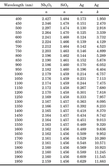
Figure1(a)shows the refractive index profile of a 32-layer design. It contains three Ag 32-layers, and the other layers are made of SiO2 or Nb2O5. The calcu-lated transmittance (solid curve) and absorption (dashed curve) of the layer system are plotted in Fig. 1(b). The transmission region covers the entire visible range (400 to 700 nm), and the final target transmittance is 50%. The average deviation from the target transmittance is about 1.5% in the trans-mission region. The transmittance in the rejection region is small, but it depends on the wavelength and is generally decreasing as the wavelength in-creases. Between 800 and 2000 nm, the calculated transmittance is less than 3:0× 10−
4and the average transmittance in this wavelength range is 9:5× 10⁻⁵. The calculations were only performed up to 2000 nm because of a lack of optical constants for the layer materials at longer wavelengths. However, from ac-tual transmittance measurements on the samples produced in our laboratory (see next section), we
know that the good rejection extends well into the far-IR spectral region. In Fig.1(b)we can see that ab-sorption in the rejection region is quite small (less than 10%). This means that more than 90% of the rejection in the rejection region can be attributed to reflection.
2. Near-IR Transmission Region
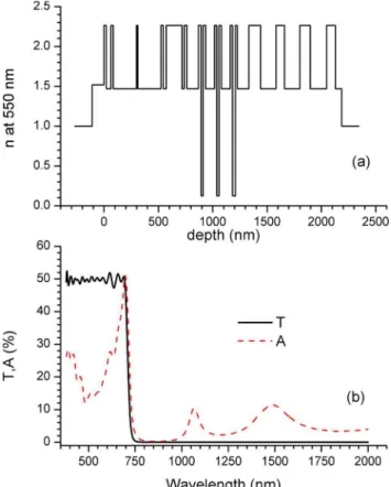
It is possible to design a long-wavelength cutoff filter with a transmission region located in a wavelength range longer than the visible part of the spectrum. How far the transition between transmission and re-jection regions can be shifted toward longer wave-lengths depends on the thickness of the Ag layers. Generally, for the same desired transmission region transmittance, thinner Ag layers will be needed for transmission regions located at longer wavelengths. It will be the discontinuous growth mode of very thin Ag layers that will set a limit on the upper wave-length at which the transition from transmission to rejection regions can occur in this type of filter. Figure 2(a) represents the refractive index profile of a long-wavelength cutoff filter with a transmission region transmittance of 44% extending from 1200 to 1580nm. Only two Ag layers are needed in this mul-tilayer because the transmission region is relatively narrow. There are 36 layers in the multilayer. The total metric thickness of the multilayer is 7:60 μm. This is much thicker than for the long-wavelength
Fig. 1. (Color online) Long-wavelength cutoff filter design with a 50% transmittance in the visible.
cutoff filter for the visible transmission region. In the rejection region (up to 3000 nm), the calculated max-imum and average transmittances are about 2:8× 10⁻⁴ and 1
:0× 10−
4, respectively. The absorption in the rejection region is also relatively small, as in the case for the filter with the visible transmission region.
3. Broad Transmission Region
By using more Ag layers, we can design a filter with an even broader transmission region. Figure3shows such a design. The transmission region extends from 390 to 1000 nm with a transmittance of about 36%. The width of the rejection region is expected to be si-milar to those of the above two examples. We can see from the refractive index profile in Fig.3(a)that the much broader transmission region is not at the ex-pense of a more complicated multilayer structure. Actually there are 33 layers in the multilayer, and the total metric thickness is only 1:74 μm. However, because the total thickness of Ag is larger, there is more absorption and, therefore, it was necessary to accept a lower transmission region transmittance. For a given transmission region transmittance, hav-ing more Ag layers also means that the thicknesses of individual Ag layers have to be thinner. So, in this case, the minimum requirement on the thickness of the Ag layers limits the width of the transmission region. The transmittance in the rejection region
(1100 to 2000 nm) of this filter decreases monotoni-cally from 3:0× 10−3 to 1
:3× 10− 5.
C. Electric Fields and Suppression and Enhancement of Transmission
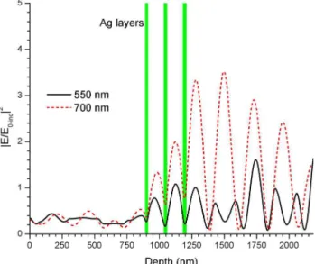
For metal/dielectric multilayers, the electric field within the multilayer structure is very critical to the filter performance. The electric field at a metal layer is directly related to the loss or absorption in the layer, and this is almost always a focal point when designing a multilayer with absorbing layers. For a cutoff filter, high transmission in the transmis-sion region requires that the electric field be as low as possible at the metal layers at the corresponding wavelengths. In the rejection region, higher absorp-tion is helpful for rejecabsorp-tion, but rejecabsorp-tion can also be realized by the high reflection. So, in a rejection re-gion, a high electric field is not necessarily an issue for cutoff filters. As we see in Figs.1–3, the absorp-tion in the rejecabsorp-tion region is actually lower than it is in the transmission region, which suggests a lower electric field. To visualize the electric field distribu-tion, we calculate the square of the electric field nor-malized to the incident electric field as a function of position within the multilayer. Figure 4 plots this quantity for the 50% visible transmission region design (Fig. 1) at two representative wavelengths in the transmission region. The vertical bars in the figure indicate positions of the Ag layers inside the multilayer. In this and the following diagram, 0 and 2200 nm on the x scale correspond to the
Fig. 2. (Color online) Long-wavelength cutoff filter design with a 44% transmittance in the near-IR spectral region.
Fig. 3. (Color online) Long-wavelength cutoff filter design with a 36% transmittance in the visible and near-IR.
substrate/multilayer and the multilayer/air inter-faces. Light is incident from the right side. We see that at both wavelengths, one at the center of the transmission region (550 nm) and the other at the cutoff edge (700 nm), there is a significant electric field distribution over the entire multilayer, although the field is generally larger on the right side of the Ag layers. Another noticeable feature for these two dis-tributions is that the electric field distribution has minimum values at the positions of the metal layers. This is also the case for almost every wavelength in the transmission region. It suggests that the numer-ical procedures optimized the multilayer structure to minimize the loss and therefore to enhance the trans-mission in the transtrans-mission region. However, it should be noted that because the optimization is for a broad wavelength range, the positions of Ag layers are not exactly located at the electric field minima. In Fig.5, the square of the electric field is plotted at two wavelengths in the rejection region. We see that the electric field only fluctuates significantly on the right side of the Ag layers. The field progressively de-creases in the Ag layers along the incident direction; i.e., less and less light penetrates each Ag layer. So, the rejection in a rejection region is much like the re-flection from a mirror. The most significant contribu-tion of absorpcontribu-tion comes from the first Ag layer where the electric field is the largest among the three Ag layers. At 1067 nm, the electric field is much lar-ger than that at 900 nm. This also means that there is a higher field in the Ag layers at 1067 nm and, therefore, more absorption at this wavelength. The small peak at 1067 nm of the absorption curve in Fig. 1(b)is the result of this high electric field.
We thus see that the rejection in the rejection re-gion is mainly due to reflection and that the
trans-mittance in the transmission region relies on induced transmission. It would be interesting to know how effective the multilayer stack is in enhan-cing these two effects. In Fig. 6(a) are plotted the transmittances of the 50% transmission region cutoff filter and that of a single Ag layer on a BK7
sub-Fig. 4. (Color online) Electric field in the transmission region of a long-wavelength cutoff filter of Fig.1. In this and the following dia-gram, 0 and 2200 nm on the x scale correspond to the substrate/ multilayer and the multilayer/air interfaces. Light is incident from the air side.
Fig. 5. (Color online) Electric field in the rejection region of a long-wavelength cutoff filter of Fig.1.
Fig. 6. (Color online) (a) Calculated transmittances in the trans-mission and rejection regions of the 50% long-wavelength cutoff filter and of a single Ag layer on a BK7 substrate. The total Ag thickness in the 50% transmission region filter is the same as that of the single Ag layer. (b) Ratio of the above two transmittances.
strate. The thickness of the single Ag layer equals the total Ag thickness in the 50% transmission region cutoff filter. We can see that in the transmission gion, the transmittance of the 50% transmission re-gion filter is much higher than that of the single Ag layer. The ratio of the two transmittances varies from 8 to 100 in the transmission region, with the largest ratio located at the cutoff edge. In the rejection re-gion, the transmittance ratio varies between 0.2 and 0.03. Thus, the multilayer stack, compared to a sin-gle Ag layer, enhances both the transmittance and the rejection in the corresponding regions by 1 or 2 orders of magnitude.
D. Some Interesting Properties of the Solutions
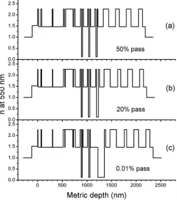
The metal/dielectric long-wavelength cutoff filter de-signs described in the above sections have some in-teresting properties. With not much more than a change of the metal layer thicknesses, one can obtain new long-wavelength cutoff designs with different transmission and rejection region transmittances. We use the visible transmission region cutoff filter to demonstrate this property. For this purpose, a ser-ies of filters was designed with the average transmit-tances in the transmission region varying from 50% to 0.0001%. The refractive index profiles of three of these filters are shown in Fig.7. We can see from this figure that the most significant difference in the mul-tilayer structure of these designs is in the Ag layer thicknesses. This is also true for the other two filter designs described in this paper. The design process is quite simple: start with an existing design, set a new
target by reducing or increasing the transmittance in the transmission region, and then optimize the mul-tilayer. This usually results in an equally good new design of different transmission and rejection region transmittances. Figure 8 shows the transmittances of these filters on a logarithmic scale. Except for the absolute values, the shapes of these transmittance curves are very similar, even though the transmit-tances in the transmission regions differ by many magnitudes.
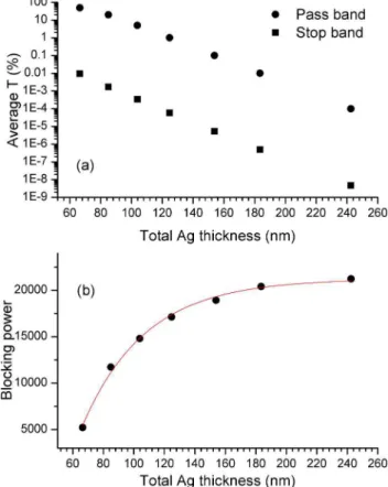
The average transmission region (400 to 700 nm) and average rejection region (800 to 2000 nm) trans-mittances are plotted in Fig.9(a)as a function of total Ag thickness. We see that on a logarithmic scale, both the average transmission and rejection region trans-mittances appear to lie on straight lines. In other words, both quantities depend on the total Ag thick-ness exponentially.
It is very interesting that such a relationship, which is similar to the behavior of a single absorbing layer, even exists for absorbing layers embedded in a complicated dielectric multilayer structure. To see some further implications of this feature, we intro-duce the concept of an average blocking power, which is defined to be the ratio of the average transmission to the average rejection region transmittances. This quantity describes the capability of the cutoff filter to block the unwanted radiation intensity relative to the desired radiation intensity. The blocking power is again plotted in Fig. 9(b) as a function of total Ag thickness. In view of Fig.9(a), it is not surprising that the blocking power has also an exponential relation-ship to the total Ag thickness. This can be clearly seen by the least-squares fit to an exponential func-tion [red line in Fig. 9(b)]. The blocking power in-creases with the Ag thickness, and for these visible transmission region long-wavelength cutoff filters, the blocking power converges toward a limiting value of 2:12× 10
4[Fig.9(b)]. For the 50% filter, the block-ing power is about 5000. Clearly, thicker Ag layers
Fig. 7. Multilayer refractive index profiles for visible transmission region long-wavelength cutoff filters with different transmission region transmittances.
Fig. 8. Set of visible long-wavelength cutoff filters with different transmittances in the transmission region.
result in higher blocking powers. However, long-wavelength cutoff filters with blocking powers close to the saturation value or very large Ag thickness will have such small transmission region transmit-tances that they will not be useful.
3. Deposition of the Long-Wavelength Cutoff Filters As already mentioned, the transmittance in both the transmission and rejection regions depends critically on the optical constants of the Ag layers. The chal-lenge in making the cutoff filters is to produce Ag layers with low n and high k values. Because the op-tical constants of the Ag layer are sensitive to deposi-tion condideposi-tions and are also thickness dependent, it is necessary to fully characterize the Ag layers before the multilayer design is finalized. Another problem related to the Ag layers is that an Ag layer can be oxidized during the deposition of the next layer. This would result in a high absorption and could comple-tely destroy the effectiveness of the Ag layer. To pre-vent this from happening, it is usually necessary to deposit a buffer layer to prevent oxidation. For exam-ple, a very thin amorphous silicon layer can be used for such a purpose. The thickness of the silicon layer is such that it is just fully oxidized during the deposi-tion of the next dielectric layer [13].
The cutoff filters were made in our magnetron sputtering system. A general description of a similar
apparatus can be found in Ref. [14]. As described in the cited paper, a broadband optical monitor was used for an in situ determination of the layer thick-nesses after the deposition of each layer. But since that paper was written, the magnetrons can now also be run with pulsed DC power supplies. It is this pro-cess that was used to produce the SiO2 and Nb2O5 layers by reactive sputtering of Si and Nb targets, re-spectively. An oxygen and argon gas mixture was used in the reactive sputtering of these two materi-als. The total pressure for the SiO2 and Nb2O5 deposition processes was 2.3 and 3:1 mTorr, respec-tively. The Ar partial pressure was about 1:0mTorr for both materials. The Ag layers were deposited in pure Ar gas at a pressure of 0:8mTorr. The pulsed DC power supply provided about 2 to 3 kW for the deposition of the dielectric layers and much less for Ag. The actual power used depended on the deposi-tion rate required in the process. As stated above, the optical properties of the Ag layers are both thickness and process dependent. However, one can also expect different Ag properties when one switches to a differ-ent multilayer design. It is important to converge onto the correct optical constants of the various thicknesses of Ag required. The Ag layers are first deposited on separate substrates, and then they are accurately measured with a spectrophotometric
Fig. 9. (Color online) (a) Transmission and rejection region trans-mittances as a function of total Ag thickness in the visible long-wavelength cutoff filters. (b) Blocking power as a function of total Ag thickness of the visible long-wavelength cutoff filters. The line is an exponential fit to the data points.
Fig. 10. (Color online) Measured transmittance of an experimen-tally produced long-wavelength cutoff filter of 50% transmittance in visible spectral region: (a) from 0.4 to 2:0 μm, measured with a spectrophotometer (the dashed curve is the calculated transmit-tance based on the layer thicknesses determined in the deposition run) and (b) from 2.0 to 20 μm, measured with an IR ellipsometer.
ellipsometer. The multilayer thicknesses are then adjusted for best performance, and the whole layer system is deposited and evaluated. Usually, several such deposition-characterization-design loops are needed before satisfactory results are obtained.
The measurements on a long-wavelength cutoff fil-ter with 50% transmission region transmittance in the visible spectral region will be described below. Figure 10(a) shows the measured transmittance (solid line) in the 0.4 to 2:0 μm spectral region of the filter. The transmittance was measured with a Perkin-Elmer Lambda 900 spectrophotometer. The dashed curve in this figure is the calculated transmittance based on the layer thicknesses determined during the deposition run. We see that the general agreement between the measured and the calculated transmit-tances is good, with all the spectral features in the measured curve explained by the calculated curve. The largest difference is in the transmission region, and it is somewhat larger than for an all-dielectric multilayer with a structure of similar complexity that is produced in the same deposition system. This is mainly because of the sensitivity of the multilayer to the uncertainty in the Ag optical constants. The transmittance in the rejection region is very small, as predicted by the calculations. For longer wave-lengths, the transmittance at normal incidence was measured using an IR ellipsometer (IR-VASE, J. A. Woollam Co., Inc.). The results between 2.0 and 20 μm are shown in Fig. 10(b). The transmittance in this spectral region is certainly less than 0.4%, because the curve is essentially the same as the noise level curve obtained when the sample was removed and the measurement beam was blocked. The fluctuations in the curve at the longer wavelength end cannot pos-sibly be explained by interference effects in the multi-layer. So the only conclusion that we can draw from the IR measurements is that the transmittance is small and that it well below the instrument noise level in this part of the spectrum.
4. Conclusions
We have shown in this paper that using the high reflectivity of Ag and the concept of induced transmis-sion, it is possible to design high-performance long-wavelength cutoff filters with wide transmission and rejection regions. The broad rejection regions are mostly due to high reflection, but absorption in the Ag also plays a part. To maximize the transmittance in the transmission region, the Ag layers are placed in locations within the multilayer structure at which the electric field strength is a minimum for wave-lengths within the transmission region in order to minimize absorption losses. The width of the trans-mission region depends on the number of Ag layers used in the design, more layers generally giving rise to a wider transmission region. The thicker the com-bined thickness of the Ag layers in a design, the lower the transmittance will be in the rejection region. A lower average transmittance in the rejection region is always accompanied by a lower average
transmit-tance in the transmission region. We define the ratio of these two average transmittances to be the blocking power of the long-wavelength cutoff filter. The prac-tical limit on the blocking power will be set by the minimum acceptable average transmittance in the transmission region. We have shown that only the thicknesses of the Ag layers need to be scaled in a long-wavelength cutoff filter design to obtain another filter with the same transmission region width but with higher or lower average transmittances in both the transmission and rejection regions.
In our experimental work, we avoided the use of Ag films thinner than 15 nm in order to ensure that the optical constants of the films are close to those of the bulk metal. In fact, the biggest challenge in the man-ufacture of such metal/dielectric coatings was to de-velop a repeatable and accurate deposition process for Ag layers with good optical constants, as also pointed out by other researchers [15]. We used DC pulsed magnetron sputtering to produce one of the long-wavelength cutoff filters and found good agree-ment between the calculated and the measured transmittance data. The measurements showed that blocking is good for wavelengths at least as high as 20 μm, and probably much higher.
In the Introduction, we referred to prior work on narrow bandpass filters based on induced transmit-tance. Because Ag has a significant extinction coeffi-cient throughout the UV, visible, and IR spectral regions, the methods described here should be equally applicable to the design of wide bandpass filters with good rejection on both sides of the transmission region.
All our design and experimental work was based on the use of thin Ag films. For long-wavelength cut-off filters with a near-UV or -IR transmission region, Al or Au films may be more suitable.
References
1. J. A. Dobrowolski, “Coatings and filters,” in Handbook of
Optics, W. G. Driscoll and W. Vaughan, eds. (McGraw-Hill,
1978), pp. 8.1–8.124.
2. H. A. Macleod, Thin Film Optical Filters, 4th ed. (CRC, 2010). 3. J. A. Dobrowolski, “Optical properties of films and coatings,” in
Handbook of Optics, 3rd ed., M. Bass, ed. (McGraw-Hill, 2010),
Vol. 4, pp. 7.1–7.136.
4. P. W. Baumeister, “Design of multilayer filters by successive approximations,” J. Opt. Soc. Am. 48, 955–958 (1958). 5. A. Thelen, Design of Optical Interference Coatings
(McGraw-Hill, 1988), p. 256.
6. J. A. Dobrowolski, L. Li, and J. Hilfiker, “Long-wavelength cut-off filters of a new type,” Appl. Opt. 38, 4891–4003 (1999). 7. Y. Guo, J. A. Dobrowolski, L. Li, D. Poitras, and J. Hilfiker, “Implementation of long-wavelength cut-off filters based on critical angle,” Appl. Opt., doc. ID 132815 (posted 16 September 2010, in press).
8. P. H. Berning and A. F. Turner, “Induced transmission in absorbing films applied to band pass filter design,” J. Opt. Soc. Am. 47, 230–239 (1957).
9. J. A. Dobrowolski, L. Li, and R. A. Kemp, “Metal/dielectric transmission interference filters with low reflectance. I. design,” Appl. Opt. 34, 5673–5683 (1995).
10. E. D. Palik, Handbook of Optical Constants of Solids I (Academic, 1985).
11. http://optilayer.com/.
12. B. T. Sullivan and J. A. Dobrowolski, “Implementation of a numerical needle method for thin-film design,” Appl. Opt. 35, 5484–5492 (1996).
13. B. T. Sullivan and K. L. Byrt, “Metal/dielectric transmission interference filters with low reflectance. 2. experimental results,” Appl. Opt. 34, 5684–5694 (1995).
14. B. T. Sullivan, G. Clarke, T. Akiyama, N. Osborne, M. Ranger, J. A. Dobrowolski, L. Howe, A. Matsumoto, Y. Song, and K. Kikuchi, “High-rate automated deposition system for the manufacture of complex multilayer coatings,” Appl. Opt. 39, 157–167 (2000).
15. H. A. MacLeod,“Anewapproachtothedesignofmetal-dielectric thin film optical coatings,” J. Mod. Opt. 25, 93–106 (1978).