Publisher’s version / Version de l'éditeur:
Green Chemistry, 12, 7, pp. 1248-1252, 2010-07-01
READ THESE TERMS AND CONDITIONS CAREFULLY BEFORE USING THIS WEBSITE. https://nrc-publications.canada.ca/eng/copyright
Vous avez des questions? Nous pouvons vous aider. Pour communiquer directement avec un auteur, consultez la première page de la revue dans laquelle son article a été publié afin de trouver ses coordonnées. Si vous n’arrivez pas à les repérer, communiquez avec nous à [email protected].
Questions? Contact the NRC Publications Archive team at
[email protected]. If you wish to email the authors directly, please see the first page of the publication for their contact information.
NRC Publications Archive
Archives des publications du CNRC
This publication could be one of several versions: author’s original, accepted manuscript or the publisher’s version. / La version de cette publication peut être l’une des suivantes : la version prépublication de l’auteur, la version acceptée du manuscrit ou la version de l’éditeur.
For the publisher’s version, please access the DOI link below./ Pour consulter la version de l’éditeur, utilisez le lien DOI ci-dessous.
https://doi.org/10.1039/c001813a
Access and use of this website and the material on it are subject to the Terms and Conditions set forth at
Green synthesis of tunable Cu(In1-xGax)Se2 nanoparticles using
non-organic solvents
Al Juhaiman, Layla; Scoles, Ludmila; Kingston, David; Patarachao,
Bussaraporn; Wang, Dashan; Bensebaa, Farid
https://publications-cnrc.canada.ca/fra/droits
L’accès à ce site Web et l’utilisation de son contenu sont assujettis aux conditions présentées dans le site LISEZ CES CONDITIONS ATTENTIVEMENT AVANT D’UTILISER CE SITE WEB.
NRC Publications Record / Notice d'Archives des publications de CNRC:
https://nrc-publications.canada.ca/eng/view/object/?id=87dc1a27-22b1-4fe9-b63a-36ac2cbce25e
https://publications-cnrc.canada.ca/fra/voir/objet/?id=87dc1a27-22b1-4fe9-b63a-36ac2cbce25e
PAPER
www.rsc.org/greenchem
| Green Chemistry
Green synthesis of tunable Cu(In
1
-x
Gax)Se
2
nanoparticles using
non-organic solvents
Layla Al Juhaiman,
a,bLudmila Scoles,
aDavid Kingston,
aBussaraporn Patarachao,
aDashan Wang
aand
Farid Bensebaa*
aReceived 28th January 2010, Accepted 29th April 2010
First published as an Advance Article on the web 27th May 2010
DOI: 10.1039/c001813a
A green synthesis route of Cu(In1-xGax)Se2nanoparticles with variable Ga content is described in
this report for the first time. Only water and a minimum amount of energy input are used. Heating appropriate amounts of Cu, In, Ga and Se dispersed in an aqueous solution containing
mercapto-acetic acid in a microwave oven gives rise to small and uniform nanoparticles. These new materials have been characterized to confirm composition, geometrical and structural properties. Transmission electron microcopy (TEM) confirmed size distribution around 4 nm. XRD confirmed the chalcopyrite structure with an average crystallite size of 3 nm. Atomic concentration and oxidation states of the different elements have been investigated using X-ray photoelectron spectroscopy (XPS). UV-visible absorption characterization confirmed the tunable optical properties of these materials. The proposed synthesis is scalable for commercial production with minimal environmental impact.
Introduction
The last two decades have seen an exponential increase of reports on nanoparticles synthesis and their potential industrial
applications.1,2The ability to produce high quality size tunable
quantum dots using wet chemical approaches3contributed to
this interest from both academia and industry. A variety of wet chemical synthesis routes have been developed, focusing mostly on the size distribution monodispersity, requiring extensive purification and size selection steps. Unfortunately the lack of scalability of these synthesis approaches and utilisation of large amount of organic solvents will continue to hinder their sustainable development and commercialisation. Development
of simple, clean and effective nanoparticle synthesis routes4,5
including the possibility of precursors separation and reuse6is
critical to fulfil the potential of these nanoparticles.
Nanoparticles are used in numerous applications to address long term environmental and energy issues. Ultra-small metallic nanoparticles are used to improve gravimetric energy density of
polymeric fuel cells.7,8Oxides nanomaterials are used to improve
photocatalysis efficiency9,10 and gravimetric energy density of
lithium ion batteries.11 Semiconductor nanoparticle are used
to form 3D heterojunctions12and high density13,14photovoltaic
films using non-vacuum coating techniques. These nanoparticles provide numerous advantages over bulk materials obtained
via conventional vacuum deposition techniques.
Nanoparticle-based coating techniques are inexpensive since they do not require high temperature and high vacuum processing. However,
aInstitute for Chemical Process and Environmental Technology National
Research Council of Canada, 1200 Montreal Rd, Ottawa, ON, K1A 0R6, Canada. E-mail: [email protected]; Tel: +1-(613) 991-6347
bChemistry Department, Science College, King Saud University,
P.O.Box. 22452, Area code 11495, Riyadh, Saudi Arabia
current fabrication processes of nanoparticles may have signifi-cant environmental impact that could negate these advantages. In recent years, numerous green chemistry approaches have been
developed to synthesize nanoparticles to address this issue.4,5,15
Often these synthesis processes have been developed to optimize utilization of bio-based precursors and to avoid organic solvents and toxic chemicals during the fabrication process. Several green techniques have been developed to produce transition metals and
group II–VI semiconductor nanoparticles.16 Other industrially
relevant photovoltaic materials have received little attention.
This is particularly the case of Cu(In1-xGax)SySe1-y (where x
and y vary from 0 to 1 and 0 to 2 respectively), often refereed as CIGS. These CIGS materials, a promising alternative to silicon solar cells and other optoelectronic applications, are currently obtained using expensive and low yield co-evaporation bulk
deposition techniques17and other particle-based techniques that
are difficult to scale.18–26
Non-vacuum fabrication techniques of CIGS film from particles precursors is presently attracting great interest from both academia and industry. Both solid state and solution-based synthesis approaches have been used in the past to produce these particles. These synthesis techniques require numerous reagents, organic solvents and reaction steps at relatively high tempera-ture with a significant amount of by-products. Reaction time, temperature, solvent and other preparation conditions are used to define the optimal synthesis process. Furthermore, obtaining small and monodispersed CIGS nanoparticles with tunable Ga
content is very important for photovoltaic applications17,27,28and
other potential applications.
Few attempts to synthesize Cu(In1-xGax)S2 or
Cu(In1-xGax)Se2 nanoparticles have been reported. Even
fewer attempts have been made to control the Ga content
within the CIGS structure.23–25 In their study, Ahn et al. used
above 15 nm.23 Using dichlorobenzene and relatively high
synthesis temperature (180 ◦C), Panthani et al. succeeded in
synthesizing CIGS nanoparticle with different Ga content.25
These processes are hardly scalable with potentially significant
negative environmental impact.4
Following our recent work,14we have used a microwave oven
to synthesize CIGS nanoparticle with variable Ga content. Numerous studies have been published on applications of
mi-crowave heating for nanomaterials synthesis.29Low microwave
processing30–32 temperature (95 ◦C) for about half an hour is
used. No organic solvent is used. Since selenium is already
incorporated in these nanoparticles, no toxic H2Se gas treatment
is required for the synthesis of the final CIGS materials.
Experimental
CuIn1-xGaxSe2 nanoparticles with x = 0, 0.25 and 0.5 were
prepared according to the following procedure. The value x corresponds to the relative percentage of Ga within the starting raw materials. Around 120 mg of copper acetate dihydrates was mixed with 300 ml de-ionized (DI) water in 500 mL round
bottomed flask. Indium chloride (InCl3) and Gallium chloride
(GaCl3) were added to the previous solution. Given the
instabil-ity of the Ga precursor in the presence of oxygen, air exposure is minimised. Solution is degassed prior to Ga addition, and
reaction was conducted under nitrogen atmosphere. The GaCl3
and Na2Se precursors were weighed in the glove box and kept
under argon gas pressure. They were used immediately by diluting in water then added to the solution according to the
description above. Except for Na2Se obtained from Alfa-Aesar,
all other chemicals were purchased from Sigma-Aldrich. After stirring the Cu and In (with or without Ga) solution for two minutes, we added 2 mL from a fresh 6 mL solution consisting of 1 ml mercapto-acetic acid and 5 mL of de-ionized (DI) water. This new solution was stirred for 5 min, then
disodium selenide (Na2Se) was added. The color of solution
turned to dark brown. The reaction vessel was transferred to the microwave oven (Mars 5X from CEM Corp. NC, equipped
with a reflux condenser) and heated to about 95◦C for 30 min.
After cooling, the solution product is centrifuged with DI water giving rise to a black powder.
After diluting the precipitate, a few drops of the resulting aqueous solution was deposited on a nickel grid and allowed to dry. TEM (transmission electron microscopy) analysis was recorded using a Philips CM20 200 kV electron microscope equipped with an Oxford Instruments energy dispersive X-ray diffraction detector. XRD characterization was performed at room temperature with Cu-Ka radiation using a Bruker diffrac-tometer D8. Powder samples were uniformly spread over a low background silicon holder.
Results
Colloidal nanoparticles obtained following microwave heating and cleaning steps are characterized to provide information about size distribution, composition and structure. In this study,
CuIn1-xGaxSe2samples with the following values of the relative
atomic concentration of Ga are synthesized and characterized:
x = 0, 0.25 and 0.5.
Fig. 1 shows TEM images of as-synthesised CuInSe2,
CuIn0.75Ga0.25Se2and CuIn0.5Ga0.5Se2nanoparticles. In all cases
sub-10 nm nanoparticles with relatively uniform size distribution are shown. The majority of the nanoparticles have an average
size of about 4 nm in the case of CuInSe2. Similar size
distri-bution has been obtained elsewhere.33CIGS nanoparticles with
higher Ga are slightly larger. It is also important to emphasize that no post-synthesis size selection has been performed. Indeed to obtain sub-10 nm nanoparticles, previous work used a large amount of different types of organic solvent to remove
larger particle sizes.33This step is not only expensive and time
consuming, but adds a negative environmental impact to the process. Furthermore, potentially significant reduction in the overall synthesis yield is expected, making these wet synthesis approaches quite prohibitive.
CIGS nanoparticle with higher Ga content showed relatively higher level of agglomeration. Presently, we can not explain why Ga-containing CIGS nanoparticles are more likely to agglomerate. Later, we will analyze the surface composition of these nanoparticles to detect any difference that could explain this trend.
Schulz et al. prepared sub-100 nm CIGS nanoparticles by reacting under nitrogen atmosphere a mixture of CuI,
InI3 and GaI3 in pyridine with Na2Se in methanol at low
temperature.13 The resulting nanoparticles are ill-defined with
diameter size ranging from 10 to 30 nm. Using a similar ap-proach, CIGS nanoparticles with a nominal chemical formulae
of Cu0.9In0.64Ga0.23Se2and average size of 20 nm have been also
reported.23,24Panthani et al. reported CIGS nanoparticle with
diameter size of 10–25 nm following a size selection step.25This
size selection step requires a large volume of different organic solvents. A solvothermal process has been also used to synthesize
CIGS nanoparticles using ethylenediamine as a solvent.34In this
case, nanoparticles with a diameter in the range of 30–80 nm
were obtained. Increasing heating temperatures up to 280◦C
for more than 24 h using this solvothermal method give rise to
larger particle size.34
In all these reports, organic solvents are used during the synthesis and also in cleaning and separation steps. Although relatively higher quality nanoparticles have previously been obtained, these organic solvents have negative environmental impact.
The average size distribution of CIGS nanoparticles obtained in this study is much lower than previously reported. Lower particle size distribution is important since they require lower temperature processing when dense films are prepared. Indeed, nanoparticle melting temperature is lowered when their diameter is reduced. The combination of uniform heating process using a microwave energy source and relatively lower processing temperature has lead to small and uniform CIGS nanopar-ticles. Microwave synthesis has been shown by this group to provide high quality Pt–Ru alloy nanoparticle with tunable
properties.30 Heating uniformity has been found to be a key
attribute of microwave synthesis of metals,30oxides31and alloyed
semiconductors32 nanoparticles. However, current microwave
design may need improvements to address potential hazards that may occur when implementing large scale productions.
To the best of our knowledge there is no report showing uniform sub-10 nm CIGS nanoparticles size distribution.
Fig. 1 TEM image of as synthesized: (a) CuInSe2, (b) CuIn0.75Ga0.25Se2
and (c) CuIn0.5Ga0.5Se2nanoparticles.
However, Castro et al. used chemical molecules containing Cu,
In, S or Se to synthesize small sub-10 nm CuInS2and CuInSe2
nanoparticles.33
Besides using size-selective step to eliminate larger particles, their structure did not include gallium.
X-Ray diffraction (XRD) has been used to characterize the structure of these as-synthesized CIGS nanoparticles. Fig. 2 shows typical diffraction features of chalcopyrite materials. Three relatively broad diffraction peaks are detected around
28, 47 and 55◦. These patterns are indicative of a chalcopyrite
tetragonal structure after comparing with the Joint Committee on Powder Diffraction Standards (JCPDS) card File No. 27– 0159. Indeed, these three peaks correspond to the (112), (220)
and (116) planes of a tetragonal structure respectively.27,28
Fig. 2 XRD spectra of CuInSe2(black solid line), CuIn0.75Ga0.25Se2(red
solid line) and CuIn0.5Ga0.5Se2(green solid line) nanoparticles.
The well-defined diffraction peak observed at 2q = 28◦ has
been used to estimate the crystallite size of these nanoparticles. The signal-to-noise ratio of the XRD spectrum is the highest around this peak. Diffractions peak width of nanoparticles are
much larger than those of bulk materials.27,28
Line broadening of the XRD diffraction peaks has been used in the past to estimate the average crystallite size of nanoparticles. Peak broadening due to instrumental artefacts and strain are not considered here.
The size of the crystallites (dc) has been determined using the
Debye-Scherrer equation:30,35
dc= 0.9 l/bcosq
whereb (in radians) is the linewidth at an angle 2q (in radians)
and l is the X-ray wavelength, 1.5406 A˚ . Based on the linewidth
of the (112) diffraction peak, we estimate the size of the crystallite to be around 3 nm. There is no significant variation in the peak linewidth using different Ga/In ratios. Thus the crystallite size does not change with Ga content.
A small but gradual peak shift is clearly observed for the (112)
peak around 2q = 28◦when Ga content is increased. Indeed, a
difference of about 0.6 degree in the peak positions of CuInSe2
and CuIn0.5Ga0.5Se2samples could be inferred from Fig. 2. This
shift is assigned to a change in lattice dimensions. This trend is consistent with Vegard’s law that support a gradual In–Ga
alloying. This has been reported on bulk27,28and nanoparticle25
Based on TEM and XRD data, we conclude that CIGS nanoparticles consist of single crystallite of 3 nm. The difference in diameter between XRD and TEM data could be assigned to a noncrystalline surface layer. Relatively larger CIGS nanopar-ticles with high Ga contents have been obtained. Indeed, an average diameter of about 4 nm or more has been estimated.
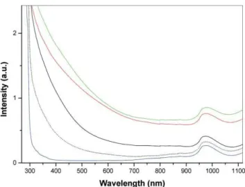
Displayed in Fig. 3 is the UV-absorption spectra of CuInS2
nanoparticles (black dotted line), CuInSe2nanoparticle (black
solid line), CuIn0.75Ga0.25Se2(red solid line) and CuIn0.5Ga0.5Se2
(green solid line). For reference purpose, UV-visible absorption spectrum of water containing surfactant is included. Absorption peak around 975 nm is assigned to water since it is also observed on pure water. We could observe an increase in
the onset of the absorption following this order: CuInS2,
CuInSe2, CuIn0.75Ga0.25Se2 and CuIn0.5Ga0.5Se2. Similar
UV-Visible absorption features are reported elsewhere on CIGS
nanoparticle.25,33–36 This could be explained by the increase
in the bandgap when substituting sulfur by selenium and/or substituting indium by gallium.
Fig. 3 UV-Visible absorption of aqueous solution (from
bottom-to-top) of: acetic-acid (blue), CuInS2(black dotted line), CuInSe2(black
solid line), CuIn0.75Ga0.25Se2(red solid line) and CuIn0.5Ga0.5Se2(green
solid line) nanoparticles.
XPS is used to evaluate the oxidation states of the different ele-ments within the CIGS nanoparticles and also characterize their surface composition. Survey XPS scans showed the presence of elements such as Cu, In, Ga and Se. Some differences in the rel-ative ratios are noticed from sample to samples. Other elements such as C and O have been also observed. The presence of these elements is assigned to the surfactant and contaminations on the surface of the nanoparticle. Although relatively high amount of mercapto-acetic acid is used, the final product does not contain significant amount of surfactant following cleaning steps. Indeed we didn’t observe any dominant Sulfur peak using XPS. In solid-state, these nanoparticle tend to agglomerate following surfactant removal. Adventitious carbon on the surface of these nanoparticles is also believed to contribute significantly to the overall XPS signal. Note that redispersion of nanoparticles in aqueous solution requires the addition of surfactant followed by stirring.
High-resolution XPS data showed the presence of single
Cu2p3/2 centered around 932.0 eV. This position is consistent
Table 1 Summary of relative atomic concentrations obtained by XPS
for three CIGS samples
CuInSe2 CuIn0.75Ga0.25Se2 CuIn0.5Ga0.5Se2
Ga 0 0.7 1.29 Cu 8.36 9.65 10.86 O 21.8 20.16 17.31 In 12.21 11.18 8.07 C 42.52 41.8 45.04 Se 15.11 16.51 17.43
with a chalcopyrite structure.37,38 Indeed Cu2p
3/2 peaks from
CuInSe2and Cu2Se with assigned positions around 931.9 and
932.8 eV respectively have been reported.38
In the case of Se3d5/2, optimal curve fitting indicates the
presence of two distinct peaks at around 54.2 and 55.2 eV. These
two peaks are assigned to Se0and Se-2species respectively. This
assignment is consistent with high resolution XPS of bulk CIGS
film reported in the literature.39It is difficult to determine the
origin of these two selenium states based solely on XPS data. We could however speculate the coexistence of two structures containing metallic and reduced selenium.
Relative atomic concentrations of these CIGS samples within the probing depth of XPS are summarized in Table 1. Carbon and oxygen are assigned to the surfactant and adventitious carbon contaminations at the surface of the nanoparticles. Values of Cu/Se ratio are estimated to be 0.55, 0.58 and 0.62 for
CuInSe2, CuIn0.75Ga0.25Se2and CuIn0.5Ga0.5respectively. It seems
that there is nearly no significant change in the value of Cu/Se for the different x values. This is consistent with XRD data that do not show any peak related to poor Cu CIGS materials
diffraction characteristics.14
Cu/(In+Ga) ratio of 0.68, 0.81 and 1.16 have been estimated
for CuInSe2, CuIn0.75Ga0.25Se2and CuIn0.5Ga0.5Se2respectively.
The trend of increased Cu/(In+Ga) as the relative amount of Ga is increased is difficult to explain. It is however possible that there is a small excess of copper rich phase at the surface of nanoparticle. Another possible explanation is the relative increase in agglomeration when Ga content is increased. Indeed TEM micrographs indicate that Ga-rich CIGS nanoparticles are agglomerated. With larger particles, copper segregation at the surface when Ga content is increased will give rise to relatively higher XPS copper signal. This is does not contradict XRD data showing a single phase on all CIGS materials. Indeed, XPS is a surface sensitive technique which is not the case of XRD.
Work is under way to replace mercapto-acetic acid surfactant with other water soluble bio-based alternatives. It will be also of interest to study the effect of other parameters such as reagents compositions and concentrations on the nanoparticles properties.
Conclusions
For the first time CIGS nanoparticle with an average size of 4 nm and variable Ga content has been synthesized without using organic solvent. These nanoparticles are stable in aqueous solution for several weeks. Size-selective step often used for quantum dot synthesis is not performed in this work. XRD data clearly showed change in lattice constant when Ga content is increased. UV-Visible data confirmed tunability of the optical
properties. Proposed synthesis approach will thus have minimal negative environmental impact since even spent water solvent could be easily recycled. Except for the surfactant, proposed synthesis satisfies the green chemistry principles. These sub-10 nm nanoparticles could be integrated in the fabrication of high density CIGS photovoltaic films and other optoelectronic applications.
References
1 Nanoparticles: From Theory to Application, ed. G. Schmid, Wiley-VCH, Weinheim, 2004.
2 H. Fukumori and H. Ichikawa, Adv. Powder Technol., 2006, 17, 1– 28.
3 C. B. Murray, D. J. Norris and M. G. Bawendi, J. Am. Chem. Soc., 1993, 115, 8706–8717.
4 J. A. Dahl, B. L. S. Maddux and J. E. Hutchison, Chem. Rev., 2007,
107, 2228–2269.
5 K. N. Thakkar, S. S. Mhatre and R. Y. Parikh, Nanomed.: Nanotech-nol., Biol. Med., 2010, 6, 257, and references therein.
6 P. T. Anastas and J. C. Warner, Green Chemistry: Theory and Practice, Oxford University, Oxford, 1998.
7 N. M. Markovic and P. N. Ross, Catal. Technol., 2000, 4, 110– 126.
8 F. Bensebaa, A. A. Farah, D. Wang, C. Bock, X. Du, J. Kung and Y. LePage, J. Phys. Chem. B, 2005, 109, 15339.
9 B. L. Abrams and J. P. Wilcoxon, Crit. Rev. Solid State Mat. Sci., 2005, 30, 153–182.
10 A. Hagfeldtt and M. Gratzel, Chem. Rev., 1995, 95, 49– 68.
11 D. R. Rolison, J. W. Long, J. C. Lytle, A. E. Fischer, C. P. Rhodes, T. M. McEvoy, M. E. Bourg and A. M. Lubers, Chem. Soc. Rev., 2009, 38, 226–252.
12 W. U. Huynh, J. J. Dittmer and A. P. Alivisatos, Science, 2002, 295, 2425–2427.
13 D. L. Schulz, C. J. Curtis, R. A. Flitton, H. Weisner, J. Keane, R. J. Matson, K. M. Jones, P. A. Parilla, R. Noufi and D. S. Ginley, J. Electron. Mater., 1998, 27, 433–437.
14 F. Bensebaa, C. Durand, A. Aouadou, L. Scoles, X. Du, D. Wang and Y. Le Page, J. Nanopart. Res., 2009, DOI: 10.1007/s11051-009-9752-5.
15 Y. Mao, T. J. Park, F. Zhang, H. Zhou and S. S. Wong, Small, 2007,
3, 1122.
16 H. Zhang, D. Wang, B. Yang and H. Mohwald, J. Am. Chem. Soc., 2006, 128, 10171–10180.
17 I. Repins, M. J. Contreras, E. B. Romero, C. DeHart, J. Scharf, C. L. Perkins and R. Noufi, Progr. Photovolt.: Res. Appl., 2008, 16, 235– 239.
18 B. M. Basol, Thin Solid Films, 2000, 361–362, 514–519.
19 V. K. Kapur, A. Bansal and O. L. Asensio, Thin Solid Films, 2003,
431–432, 53–57.
20 C. Eberspacher, C. Frederic, K. Pauls and J. Serra, Thin Solid Films, 2001, 387, 18–22.
21 M. Kaelin, D. Rudmann, F. Kurdesau, T. Meyer, H. Zogg and A. N. Tiwari, Thin Solid Films, 2003, 431–432, 58–62.
22 M. Kaelin, D. Rudmann, F. Kurdesau, T. Meyer, H. Zogg and A. N. Tiwari, Thin Solid Films, 2005, 480–481, 486–490.
23 S. J. Ahn, K. H. Kim and K. H. Yoon, Colloids Surf., A, 2008, 313–
314, 171–174.
24 S. J. Ahn, K. H. Kim, Y. G. Chun and K. H. Yoon, Thin Solid Films, 2007, 515, 4036–4040.
25 M. G. Panthani, V. Akhavan, B. Goodfellow, J. P. Schmidtke, L. Dunn, A. Dodabalapur, P. F. Barbara and B. A. Korgel, J. Am. Chem. Soc., 2008, 130, 16770–16777.
26 C. J. Carmalt, D. E. Morrison and I. P. Parkin, J. Mater. Chem., 1998, 8, 2209–2211.
27 V. Alberts, Mater. Sci. Eng., B, 2004, 107, 139–147. 28 V. Alberts, Thin Solid Films, 2009, 517, 2115–2120.
29 G. A. Tompsett, W. C. Conner and K. S. Yngvesson, ChemPhysChem, 2006, 7, 296–319, and references therein.
30 F. Bensebaa, N. Patrito, Y. Le Page, P. L’Ecuyer and D. Wang, J. Mater. Chem., 2004, 14, 3378–3384.
31 F. Bensebaa, F. Zavaliche, P. L’Ecuyer, R. W. Cochrane and T. Veres, J. Colloid Interface Sci., 2004, 277, 104–110.
32 V. Firth, Y. Tao, D. Wang, J. Ding and F. Bensebaa, J. Mater. Chem., 2005, 15, 4367–4372.
33 S. L. Castro, S. G. Bailey, R. P. Raffaelle, K. K. Banger and A. F. Hepp, J. Phys. Chem. B, 2004, 108, 12429–12435.
34 Y. G. Chun, K. H. Kim and K. H. Yoon, Thin Solid Films, 2005,
480–481, 46–49.
35 C. Czekelius, M. Hilgendorf, L. Spanhel, I. Bedja, M. Lerch, G. Muller, U. Bloeck, D. S. Su and M. Gersig, Adv. Mater., 1999, 11, 643–646.
36 J. J. Nairn, P. J. Shapiro, B. Twamley, T. Pounds, R. von Wandruszka R, T. R. Fletcher, M. Williams, C. Wang and M. G. Norton, Nano Lett., 2006, 6, 1218–1223.
37 J. Llanos, A. Buljan, C. Mujica and T. J. Ramirez, J. Alloys Compd., 1996, 234, 40–42.
38 E. P. Domashevskayaa, V. V. Gorbachev, V. A. Terekhova, V. m. Kashkarova, E. V. Panfilova and A. V. Shchukarev, J. Electron Spectrosc. Relat. Phenom., 2001, 114–116, 901–908.
39 B. Canava, J. Vigneron, A. Etcheberry, J. F. Guillemoles and D. Lincot, Appl. Surf. Sci., 2002, 202, 8–14.