HAL Id: hal-02157332
https://hal.archives-ouvertes.fr/hal-02157332
Submitted on 7 Nov 2020
HAL is a multi-disciplinary open access
archive for the deposit and dissemination of
sci-entific research documents, whether they are
pub-lished or not. The documents may come from
teaching and research institutions in France or
abroad, or from public or private research centers.
L’archive ouverte pluridisciplinaire HAL, est
destinée au dépôt et à la diffusion de documents
scientifiques de niveau recherche, publiés ou non,
émanant des établissements d’enseignement et de
recherche français ou étrangers, des laboratoires
publics ou privés.
Sub-nanosecond delay CMOS Active Gate Driver for
Closed-Loop dv/dt Control of GaN Transistors
Bau Plinio, Marc Cousineau, Bernardo Cogo, Frederic Richardeau, Vinnac
Sébastien, Didier Flumian, Nicolas Rouger
To cite this version:
Bau Plinio, Marc Cousineau, Bernardo Cogo, Frederic Richardeau, Vinnac Sébastien, et al..
Sub-nanosecond delay CMOS Active Gate Driver for Closed-Loop dv/dt Control of GaN Transistors.
31st IEEE International Symposium on Power Semiconductor Devices and ICs (ISPSD), May 2019,
Shanghai, China. �10.1109/ispsd.2019.8757693�. �hal-02157332�
Email: [email protected]
[email protected]
Abstract— This paper presents an AGD (active gate driver) implemented with a low voltage CMOS technology to control the
dv/dt sequence of low voltage (100V) and high voltage (650V) GaN power transistors. Such an AGD can control and reduce the dv/dt of fast switching GaN devices with a reduced impact on switching losses. In the case of both low voltage and high voltage GaN fast switching transistors, such an AGD must have a total response time lower than 1ns. Therefore, introducing a feedback loop to control the dv/dt requires a specific design with a very high bandwidth (550MHz). Moreover, probing the vDS voltage and its derivative is
quite challenging, as the voltage level is higher than the low voltage gate driver supply. The purpose of this work is to optimize a low voltage CMOS AGD with fully integrated functions, and implement such a solution in GaN-based power converters.
Keywords—Active gate driver, GaN, switching analysis, dv/dt, EMI, power electronics, ASIC for power ic.
I. INTRODUCTION
Different solutions have been previously demonstrated to control separately the dv/dt and di/dt sequences with silicon, SiC and GaN FETs in the view of improving the loss versus EMI tradeoff. Different strategies to improve this tradeoff are: a variable impedance output stage, an open-loop control with previously programmed, an adjusted impedance sequence [1-5] or a closed-loop control to reduce the gate current during the dv/dt sequence [6,7]. The open-closed-loop solutions rely on pre-optimization and fine tuning of the variable impedance switching sequence, which can be sensitive to parameter dispersion [1-5]. Closed-loop controls are either based on discrete components [6,7] or integrated solutions [3]. The discrete solutions typically have a large response time, above few nanoseconds or tens of nanoseconds. Our approach consists to get a full CMOS integration for all the required functions. The size of the high voltage capacitor required to sense the dvDS/dt has been reduced to a few pico-Farads, which can
be integrated on-chip in our work. This method can be used both for turn-on and turn-off transients. However, the first developments concern only the active control of the turn-on transient. The turn-off sequence is typically controlled by the output load current in the case of high switching speed (low switching losses), and the Zero Voltage Switching (ZVS) condition is more critical than the turn-off switching speed, in the case of synchronous buck converter [8]. However, it should be mentioned that the proposed active gate driver can be easily modified to actively control the turn-off of a fast switching GaN transistors using the exact same principle as the one detailed hereafter.
II. PRINCIPLE OF THE ACTIVE GATE DRIVER
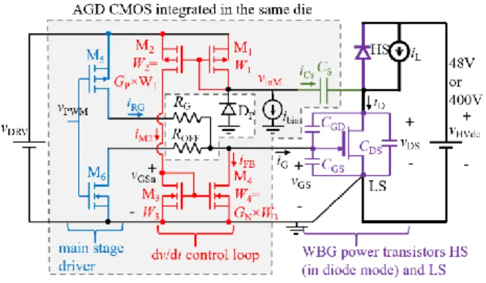
Fig. 1 shows the transistor level schematics of the proposed CMOS AGD. Additionally, to the required output buffer (M5-M6), a high voltage sense capacitor CS and a two stage current mirror M1-M2 and M3-M4 are integrated. During the dv/dt
sequence, the dv/dt sense current iCs is amplified and participates to reduce the gate current ig during the Miller plateau (Fig. 2).
Consequently, the dv/dt is reduced, while keeping a fast di/dt sequence unchanged. The trade-off between dv/dt and the turn-on energy loss EON is then optimized, comparatively to a change of the gate resistor RG, as already demonstrated [6,7].
Author version of the accepted article published in the IEEE proceedings ISPSD2019 –
https://doi.org/10.1109/ISPSD.2019.8757693
Fig. 1. CMOS AGD topology in a transistor level schematic.
As presented earlier, the transistors M1-M6 are 5V transistors which are particularly suited to drive efficiently EPC GaN transistors, and can also drive GaN systems transistors, albeit with non-optimal driving voltages. The transistors M5 and M6 are designed with a +/-3A source/sink current rating, with integrated pre-amplification and short-circuit protection. DP is a protection
diode to prevent the current mirror input voltage vinM from achieving values outside the safe operating region of the transistor
M1. ibias is a current source improving the response time of the feedback loop, which will be further discussed in section IV.
Fig. 2 shows the qualitative current and voltage waveforms during a turn-on of the GaN power device. This time interval can be divided into the di/dt (between t1 and t2) and the dv/dt (between t2 and t3) sequences. The time duration tD-t2 is the feedback
loop delay, further analyzed in section IV.
Fig. 2. Qualitative waveforms for gate voltage and currents with the AGD during turn-on (closed-loop). (a) Current and voltage at the power gate and (b) currents being supplied and sinked simultaneously by the AGD.
The main idea of this method is to emulate a virtual capacitor added between the gate and drain nodes of the power device only during the dv/dt phase. The value of such an equivalent capacitor can be controlled by the gain G of the feedback loop (gain of the cascaded current mirrors M1-M2 and M3-M4). One should note that this gain G results from the first stage PMOS transistors and the second stage NMOS transistors G = GP × GN. The emulated capacitance effect occurs when a feedback current
iFB is sinking from the gate of the power device during the dv/dt phase. This feedback current is generated by the current mirror
gain G and the CS sense capacitor value. This added emulated capacitance equal to GCS can be easily computed using a simplified
model for the power transistor where the dv/dt of the power device is expressed by (1): d𝑣DS d𝑡 = − 𝑣DRV−𝑣M 𝑅G𝐶GD + 𝑖FB 𝐶GD= − 𝑣DRV−𝑣M 𝑅G(𝐶GD+𝐺𝐶S) (1)
where vDRV is the power supply voltage of the driver and vM is the Miller plateau voltage, shown in Fig. 2.
This principle has been previously and successfully applied to the control of Silicon IGBT [6] and high voltage GaN FET [7] for which the turn-on time is significantly high. However, this closed-loop approach is particularly difficult to achieve when GaN
Reduction in | dV/dt | 1.8 to 0.5V/ns 27 to 8V/ns 45 to 6.6V/ns vHVdc 600V 300V 400V and 48V vDS fall time during turn-on 333ns 11ns 20ns and 4ns Embedded in an ASIC No No Yes III. IMPLEMENTATION A. CMOS AGD
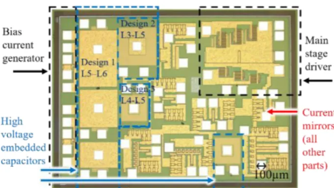
Fig. 3 shows a microscope photograph of the fabricated AGD in AMS 180nm CMOS technology. This first prototype has been designed as a test chip with several current mirror designs and embedded high voltage capacitors. Even though quite simple, the design of the current mirrors is subject to important compromises such as the feedback loop gain splitting between the CS
value, the first and second current mirror stage gain values, the large maximum output current in M4, the dynamic bias current
ibias and the M2-M3 biasing during the active driving. Key constraints are current consumptions, total silicon area (embedded
capacitor + current mirrors) and bandwidth. These design considerations will be illustrated in section IV. After a quick characterization in probe station [9], the AGDs are packaged in QFN24 6mm×6mm. The packaged AGDs are then implemented to drive commercially available low voltage and high voltage GaN FETs.
Fig. 3. Optical microscope photograph of the CMOS AGD test chip built in 0.18µm technology.
B. Implementation in 48V and 400V DC bus voltages
Two different boards have been developed to demonstrate the active control of GaN transistors in 48V and 400V applications. In both experiments, only the low side (LS) GaN transistor is driven by our CMOS AGD, while the high side (HS) GaN transistor has its gate and source shorted. The 4-layer PCB (48V) and 6-layer PCB (400V) have been designed to minimize the gate and power loops, hence only voltage probes are used. In this first implementation, an external CS ceramic capacitor is used, 2pF/250V
for 48V (J0603D2R0BXPAJ) and 1pF/500V for 400V (MC0805N1R0C501CT).
Fig. 4 (a) shows the system implementation in a 48V-36A power commutation cell with EPC2001 eGaN™FET. Fig. 4 (b) shows a similar implementation in a 400V-30A application, with GaN systems e-mode GS66508T transistors. Additional components are limited to decoupling capacitors, protection and configuration buffers and gate resistors.
Author version of the accepted article published in the IEEE proceedings ISPSD2019 –
https://doi.org/10.1109/ISPSD.2019.8757693
Fig. 4. AGD in a half bridge configuration for test in double pulse for (a) 4-layer board with 48V DC bus voltage with 100V GaN EPC 2001C device. (b) 6-layer board with 400V DC bus voltage with 650V GaN systems GS66508T devices.
C. Experimental Results
In the case of 48V bus voltage, the dv/dt is attenuated from 15V/ns to 6.3V/ns with the CMOS AGD (Fig. 5). Simulation results shows the switching losses are increased from 1.93µJ to 2.34µJ during turn-on. Cadence™ simulation results fitting experimental data shows the switching losses are reduced by 15.7% comparing to the increase of the gate resistance RG, while
keeping the same attenuation in dv/dt. For the 400V application, the dv/dt is attenuated from 45V/ns to 6.6V/ns, (Fig. 6). Both cases use RG = 4.4Ω. This choice of RG has been made for the EPC2001C because characterization tests in open-loop with lower
values showed no more significant increase in peak dv/dt with lower RG values. For 400V tests, the same value is used for
comparative purposes.
Fig. 5. Experimental results with the CMOS AGD in the 48V DC bus voltage. With the closed-loop, the dv/dt is attenuated from 15V/ns to 6.3V/ns.
bias
able to provide a very fast response for any external transient. Table I shows the results obtained with Cadence™-Spectre™ transient simulations to determine the value of the delay defined in Fig. 2 for different biasing currents ibias. Different total gain
values (5, 10, 20 and 50) for the current mirrors are simulated and implemented within the prototype. One has to note that all transistors M1-M4 are designed differently for each case of total gain G value. If different gain modifies the dv/dt in closed-loop and consequently the input current iCs, it also implies different parasitic capacitance values which impact the overall
response time. In these simulations, for comparison purpose, a constant dv/dt equal to 15V/ns with a sense capacitor of 2pF is considered. The design must be done carefully, splitting the total gain G into two different gain GP and GN to minimizing the
parasitic capacitors of the transistors, leading to an optimized size reducing the several time constants of the feedback loop.
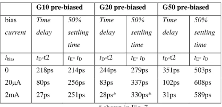
TABLEII
SIMULATED RESPONSE TIME FOR DIFFERENT VALUES OF BIASING CURRENT WITH THREE DIFFERENT GAINS
G10 pre-biased G20 pre-biased G50 pre-biased bias current Time delay 50% settling time Time delay 50% settling time Time delay 50% settling time ibias tD-t2 tE- tD tD-t2 tE- tD tD-t2 tE- tD 0 218ps 214ps 244ps 279ps 351ps 503ps 20μA 80ps 256ps 83ps 337ps 102ps 608ps 2mA 27ps 251ps 28ps* 330ps* 31ps 589ps * shown in Fig. 7
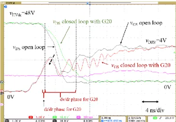
The time intervals tD–t2 and tE–tD are determined on Fig. 7 showing a simulation of the response time with the current mirror
G = 20 pre-biased with a 2mA ibias current. The input current goes from 0 to 26mA that correspond to a dv/dt equal to either
26V/ns with CS = 1pF or 13V/ns with CS = 2pF.
After tens of picoseconds the feedback loop provides a current at the output (iFB) and therefore is already acting and affecting
the dv/dt.
The delay decreases as the bias current ibias increases. This improvement is at the expense of an additional power
consumption. Indeed, using a pre-bias current, extra losses in transistors M1 to M4 are generated, which can reach high levels due to the high value of the gain GP. It should be noted that, this biasing current can be provided only during the switching.
Author version of the accepted article published in the IEEE proceedings ISPSD2019 –
https://doi.org/10.1109/ISPSD.2019.8757693
Fig. 7. Simulation of the transient response time with G = 20 (vDRV = 4V, ibias = 2mA, iCs = 30mA).
B. Bandwidth analysis
If a non-null current ibias is used to pre-bias the two current mirrors, a small signal analysis can be performed to determine the
bandwidth of the feedback loop. Fig. 8 shows the equivalent circuit required for the study in the frequency domain. The input signal is the current coming from the capacitor CS during a turn-on event assuming that a constant dv/dt occurs during the
transient. The output of the second stage is connected to the resistance RG and the gate of the power device behaving like a
voltage-dependent capacitor CISS during the Miller’s plateau. Small signal models of transistors M1 to M4 are used in Fig. 8:
Fig. 8. Small signal analysis of the AGD current mirrors during dv/dt phase.
The current gain transfer function is expressed by (2).
𝐼FB(𝑠) 𝐼Cs(𝑠)= 𝐺𝑃𝐺𝑁 1−𝐶GD2 𝑔m2𝑠 1+𝜏21𝑠 . 1−𝐶GD4 𝑔m2𝑠 1+𝜏43𝑠 (2)
where GP and GN are respectively the gains of the current mirrors M1-M2 and M3-M4, gmi and gDSi respectively the
transconductances and the drain-to-source admittances of transistors M1 to M4, τ21 and τ43 the time constants of both current
mirrors.
The mirror time constants are calculated with the following expressions:
𝜏21= 𝐶1 𝑔m1; 𝜏43= 𝐶2 𝑔DS2+𝑔m3 (3) with { 𝐶1= 𝐶DP+ 𝐶DS1+ 𝐶GS1+ 𝐶GS2+ 𝐶GD2(1 + 𝑔m2 𝑔DS2+𝑔m3) 𝐶2= 𝐶DS2+ 𝐶DS3+ 𝐶GS3+ 𝐶GS4+ 𝐶GD4(1 + 𝑔m4 𝑔DS4+𝑅G1 )(4)
where CDP is the capacitive contribution of the reverse biased protection diode DP.
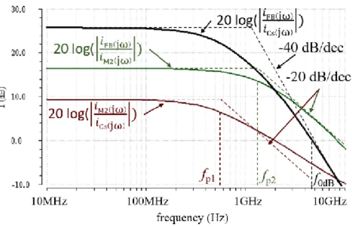
A Cadence™ AC simulation (Fig. 9) demonstrates a bandwidth close to 550MHz (-3dB gain) for the two-step current mirror with a current gain G = 20 and considering an input current made of a biasing current ibias = 2mA increased by a 12mA current
V. EMBEDDED CAPACITOR FOR DV/DT SENSING
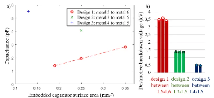
In order to propose a fully integrated solution, high voltage pF range CS capacitors are integrated on chip. The different
designs involve different metal and oxide layers offered by the CMOS technology. The design compromises are the capacitor density, the breakdown voltage and the common mode parasitic capacitor. The breakdown voltages of three different designs are measured between 500V and 3.5kV (Fig. 10). The measurements have been done in a probe station under vacuum. For low voltage applications (48V), 5.5pF are measured with a surface of 0.13mm² and a destructive breakdown at 450V. For medium voltage applications (400V), 1.3pF to 2.9pF are measured for a surface of 0.19mm² to 0.35mm² respectively. The destructive breakdown for those capacitors occurs at 3.5kV. These measurements confirm the viability of a full CMOS integration of our solution.
Fig. 10. High voltage embedded capacitor integration measurements for the proposed method (a) capacitance (b) breakdown voltage (L3 to L6 are the metal layer of the technology).
VI. CONCLUSION
A solution to reduce the dv/dt value while saving switching loss is presented and fully integrated in CMOS technology. 15.7% EON switching energy is saved compared to a simple reduction in dv/dt by changing the gate resistance. A high bandwidth
is demonstrated both theoretically and experimentally for the feedback loop, showing sub-nanosecond delays. The experimental characterizations show the effectiveness of the active dv/dt control of fast switching GaN power transistors both for 48V and 400V applications. The key benefits of our technique are: a fully CMOS integrated solution, a reduced overcurrent during turn-on, an improved EMI vs switching-loss tradeoff, simple and fast analog circuits to implement a closed-loop technique and the possibility to integrate pF range high voltage capacitor used as a dv/dt sensor. Next steps will be the integration of continuously variable feedback gains and further optimization both in design and topology.
REFERENCES
[1] M. Takamiya, K. Miyazaki, H. Obara, T. Sai, K. Wada and T. Sakurai, "Power electronics 2.0: IoT-connected and Al-controlled power electronics operating optimally for each user," 2017 29th International Symposium on Power Semiconductor Devices and IC's (ISPSD), Sapporo, 2017, pp. 29-32.
[2] M. Rose, Y. Wen, R. Fernandes, R. Van Otten, H. J. Bergveld and O. Trescases, "A GaN HEMT driver IC with programmable slew rate and monolithic negative gate-drive supply and digital current-mode control," 2015 IEEE 27th International Symposium on Power Semiconductor Devices & IC's (ISPSD), Hong Kong, 2015, pp. 361-364. [3] J. Yu, W. J. Zhang, A. Shorten, R. Li and W. T. Ng, "A smart gate driver IC for GaN power transistors," 2018 IEEE 30th International Symposium on Power Semiconductor
Devices and ICs (ISPSD), Chicago, IL, 2018, pp. 84-87.
Author version of the accepted article published in the IEEE proceedings ISPSD2019 –
https://doi.org/10.1109/ISPSD.2019.8757693
[4] H. C. P. Dymond et al., "A 6.7-GHz Active Gate Driver for GaN FETs to Combat Overshoot, Ringing, and EMI," in IEEE Trans. on Power Elect., vol. 33, no. 1, pp. 581-594,
Jan. 2018.
doi: 10.1109/TPEL.2017.2669879.
[5] Shihong Park and T. M. Jahns, "Flexible dv/dt and di/dt control method for insulated gate power switches," Conference Record of the 2001 IEEE Industry Applications
Conference. 36th IAS Annual Meeting (Cat. No.01CH37248), Chicago, IL, USA, 2001, pp. 1038-1045 vol.2.
[6] B. Sun, R. Burgos, X. Zhang and D. Boroyevich, "Active dv/dt control of 600V GaN transistors," 2016 IEEE Energy Conversion Congress and Exposition (ECCE), Milwaukee,
WI, 2016, pp. 1-8.
doi: 10.1109/ECCE.2016.7854818.
[7] R. Grezaud, F. Ayel, N. Rouger and J. Crebier, "A Gate Driver With Integrated Deadtime Controller," in IEEE Trans. on Power Elect., vol. 31, no. 12, pp. 8409-8421, Dec. 2016.
doi: 10.1109/TPEL.2016.2517679.
[8] P P. Bau, M. Cousineau, B. Cougo, F. Richardeau, D. Colin and N. Rouger, "A CMOS gate driver with ultra-fast dV/dt embedded control dedicated to optimum EMI and turn-on losses management for GaN power transistors," 2018 14th Cturn-onference turn-on Ph.D. Research in Microelectrturn-onics and Electrturn-onics (PRIME), Prague, 2018, pp. 105-108.