Advanced Silicon Photonic Modulators
by
Cheryl M. Sorace
Submitted to the Department of Electrical Engineering and Computer Science in partial fulfillment of the requirements for the degree of
Master of Science in Electrical Engineering and Computer Science at the
MASSACHUSETTS INSTITUTE OF TECHNOLOGY
September 2010
C Massachusetts Institute of Technology 2010. All rights reserved.
ARCHIVES
0
CT 3 5 2Z
~ TA uthor...
Department of Electrical Engineering and Computer Science September 3, 2010
a .' / I
Certified by... ...
A ccepted by ...
Franz X. Kartner Professor of Electrical Engineering Thesis Supervisor
,1 ~
Terry P. Orlando Chairman, Department Committee on Graduate Students
ADVANCED SILICON PHOTONIC MODULATORS
by
CHERYL SORACE
Submitted to the Department of Electrical Engineering and Computer Science on September 3, 2010 in partial fulfillment of the
requirements for the degree of Master of Science in Electrical Engineering and Computer Science
Abstract
Various electrical and optical schemes used in Mach-Zehnder (MZ) silicon plasma dispersion effect modulators are explored. A rib waveguide reverse biased silicon diode modulator is designed, tested and found to operate at speeds up to 13 GHz with a V"L of 1.2 Vcm. MOS capacitor modulator designs are investigated as an alternative, but are not found to offer significant advantages. Modulators are also designed for fabrication in an actual CMOS process -a crucial step in the quest for low-cost integration with modern electronic devices. Photonic crystal structures, which promise smaller footprint sizes and lower power requirements, are also investigated, but it proves difficult to obtain a physically feasible design. Finally, a linearization scheme for Mach-Zehnder modulators is proposed to significantly improve signal fidelity in analog applications. Simulations are used to demonstrate the effectiveness of this scheme for reverse biased silicon diode modulators.
Thesis Supervisor: Franz X. Kartner
ACKNOWLEDGEMENTS
First, I'd like to thank my advisor, Franz X. Kartner, for all his fantastic guidance and for giving me the opportunity to work on this project. He has been a patient mentor, a receptive sounding board, and an invaluable source of direction in my research.
So far at MIT, I've had the opportunity to work with many wonderful people and I'd like to express my gratitude to them. Anatoly Khilo, especially, has been my go-to person for patiently explaining everything from basic physical concepts to MIT logistics. He should really be a coauthor on the Linearity Section. I am also grateful to Amir Nejadmalayeri for his valuable explanations and experimental help. Jason Orcutt from Rajeev Ram's group has also provided me with helpful insights and many fruitful conversations. Additionally, I'd like to thank him for letting me borrow his measurement setup. I'd like to thank Dorothy and Donna for all the behind the scenes work that keeps the group running smoothly. Special thanks, or maybe recriminations, go to Dorothy for fueling my mid-afternoon candy habit. Finally, I'd like to thank all the
members of the OQE group for making my time so far enjoyable and productive. I look forward to continuing to work with them.
I'd also like to thank our collaborators at Lincoln Laboratory; Dr. Steven Spector, Dr.
Michael Geis, Dr. Matthew Grein, and Dr. Jade Wang, for the countless hours they have spent working on this project with us, and particularly for fabricating our devices and for
characterizing many of them.
Additionally, I'd like to thank all the wonderful teachers I have had a Cornell and MIT that have prepared me so well for research. In particular, I'd like to thank Professor David Muller for all his advice, and Professor Michel Louge for giving me a great undergraduate introduction to research.
I'd like to thank my friends and family for all the incredible support they have provided me
over the years. I'd especially like to thank Kendra for being my voice of reason, Tom for always seeing the bright side, and LEM for providing me with my first MIT home. Finally, I'd like to thank my fiance, Ameya, for celebrating the good times with me and pulling me through the bad times.
SUPPORT
This work was funded by DARPA as part of the EPIC program and by a National Science Foundation Graduate Research Fellowship. Additional support was provided by the MIT Ida M. Green Fellowship.
CONTENTS
IN TR O D U C T IO N ... 11 A PPLICATIONS OF M ODULATORS...1 Photonic AD C Converters ... I I SILICON PHOTONICS...13 SCOPE OF THESIS ... 15 M O D U LA TO R BA SIC S...16PHYSICAL EFFECTS U SEFUL FOR M ODULATION ... 16
Pockels and K err Effects...16
Quantum Confined Stark Effect and Franz-Keldysh Effect... .... 16
Therm o-Optic Effect...17
Plasm a-D ispersion Effect ... 17
MACH-ZEHNDER MODULATORS - RATIONAL AND TRANSFER FUNCTION ... 19
FIGURES OF M ERIT...22
FUNDAMENTAL LIMITATIONS OF PLASMA-DISPERSION MZ MODULATORS... ... 22
M O D U LA TO R M O D ELIN G ... 29
ELECTRICAL SIM ULATION D ETAILS ... 30
O PTICAL SIM ULATION D ETAILS ... 33
RIB WAVEGUIDE MZ MODULATOR DESIGNS ... 36
M ODAL O VERLAP CONSIDERATIONS ... 36
A CTIVE D EVICES FOR M OVING CARRIERS ... 40
D iode M odulators ... 41
M OS Capacitor M odulators ... 54
Other Modulator Electrical Structures in the Literature ... ... 63
LINEARIZATION OF MZ MODULATORS... 64
SCHEM E PROPOSED IN THIS W ORK...64
APPLICATION OF SCHEME TO REVERSE BIASED SILICON MZ MODULATOR...70
MZ MODULATORS IN THE NATIVE CMOS PROCESS ... 75
PH O TO N IC C R Y STA L M O D U LA TO R S...83
BACKGROUND...83
USE AS SLOW WAVE STRUCTURES AND SLOW WAVE MODULATORS...87
SLOW -W AVE M ODULATOR D ESIGN ... 89
A chievable Slowdown ... 89
Contacting Issues...93
C O N C LU SIO N S A N D FU T U R E W O R K ... 97
A PPEN D IC ES...98
A : SELECT PARAM ETERS U SED IN ELECTRICAL SIM ULATIONS ... 98
B : EXAM PLE ELECTRICAL SIM ULATION CODE ... 103
C : O PTICAL PROCESSING CODE ... 109
D : EXAM PLE "M IT PHOTONICS BANDS" CODES ... 118
INTRODUCTION
Applications of Modulators
As electronics become more complex and performance demands become more exacting, it becomes increasingly important that each component in a system be as accurate and efficient as possible. Sometimes the performance of traditional electrical components is acceptable for the desired specifications. Increasingly, however, the use of non-traditional components is necessary or will be necessary to meet performance targets [1]. Optical components, in particular, provide a path forward towards achieving much-desired performance gains. Including optical components in a system, however, requires successfully passing the requisite information back and forth between the optical and the electrical components in the system. Such communication is accomplished by the use of photodetectors, which allow optical signals to be passed to electrical systems, and modulators, which pass electrical signals to optical systems. While any photonic link would need to consist of both a modulator and a photodetector, this work will be
focused on the design and implementation of electrical to optical modulators.
There are many applications in which opto-electronic integration is desirable. One such application is communication between multiple processing cores and memory modules in integrated circuits, particularly when these components are located on different chips, or far apart on the same chip. Currently data transmission between these components is accomplished via electrical interconnects. However, as transistor density and the bandwidth required increase, power density and interconnect latency become problematic. Photonic links are likely to be faster, have higher bandwidth, and use less power than traditional electronic solutions [1].
Photonic ADC Converters
ADCs are the means by which analog signals (from, say, an imaging system or an antenna) are digitized for further processing. Many different effects, including thermal effects, ambiguity, quantum uncertainty and jitter, place limits on the performance of ADC systems [38]. These limits for available technologies are summarized in Figure 1, which also summarizes the performance of current electronic ADCs. As can be seen, aperture jitter - random deviation from the nominal sampling period - is the effect that currently limits electrical ADC performance. At present, aperture jitter in electronic ADCs is on the order of 100 fs and improves only slowly [7]. Optical sources can be much more precisely timed, with jitters of less
than 100 attoseconds, and, therefore, offer a way around this problem. Optical schemes to implement or improve ADC performance have been around for several decades, but only recently have mode-locked lasers been stable enough for these schemes to be practical [7]. Optical ADC schemes generally fall into one of four categories: (1) where photonics simply "assist" an existing electrical component, (2) where optics are used to sample and electronics to quantize the signal, (3) the reverse, where optics quantize and electronics sample the signal, and (4) where optics are used to both quantize and sample the signal [39].
20
14-110
8 E
0"
1.E+04 1.E+.05 1.E+06 1.E+07 1.E+08 1.E+.09 1.E+1D 1,E+11 Analog Input Frequency (Hz)
Figure 1: Performance of electrical ADC and performance limits. From [38].
Our group is currently working on designing an ADC of the second type; in which optical sampling is combined with electrical quantization. The optical sampling allows for a significant increase in the ADC bandwidth at a given accuracy. Specifically, the
jitter
problem is overcome by the use of a stable mode-locked laser to determine the sampling times, thus increasing the timing precision, and by the use wavelength division multiplexing (WDM) to split the signal between several electronic ADCs and thereby multiply the effective sampling rate achievable at a given ENOB level. To be more precise, a mode locked laser and a dispersive fiber are used to generate a sequence of chirped pulses. An electro-optic modulator, driven by the RE signal to besampled, imprints the signal on the chirped pulse stream. The modulated signal is then passed through an optical filter bank where different channels pick out the different frequencies of the chirp. Each channel passes its frequency to a photodetector, which converts it back into an electrical signal. Finally, this electrical signal is quantized using an electronic ADC. Because the temporal relationship between the frequencies is known, the digital output from all of the different channels can be stitched back together to create a finely-sampled version of the signal. The sampling rate of the ADC is then that of the electronic ADCs multiplied by the number of different channels of the filter bank [7]. For example, if the system had 20 channels and each channel had an electrical ADC sampling at 2 GHz, the overall sampling rate would be 40 GHz. The achievable ENOB could then be as high as the 8-10 effective bits 2 GHz electrical ADCs can achieve, instead of the 4 or so effective bits higher speed electronic ADCs can obtain [38].
Mode-locked Dispersive laser fi0be -' 0 00 Bandpas
O
O..
s filter MZ modulator 0 0 O SAIDC Figure 2 Schematic of optically sampled, electrically quantized ADC. Knowledge of the precise temporal location of each different optical frequency allows the outputs from all of the electronic ADCs to be recombined to yield a finely sampled version of the original signal. From [7].Silicon Photonics
Much attention has been paid to silicon photonics because it promises to integrate optical and electronic devices together on the same chip, or even optical and electronic functions into the same device. Such integration would allow for the cheap, efficient and effective use of optics to improve the performance of what are presently all-electronic systems where the electronics are hitting their fundamental performance limits. Additionally, silicon photonic structures can take advantage of silicon fabrication techniques that have been developed into maturity for the electronics industry [5]. This allows silicon photonic devices to be made easily and cheaply.
There are other reasons that silicon is a good candidate for optical device design. The high index contrast between silicon and air, or, more importantly, between silicon and its native oxide
(SiO2) allows for high index contrast (HIC) waveguides to be easily fabricated. HIC structures have the advantage of tight confinement (which decreases necessary power), small size and a tight bending radius (which decreases device size-key for any sort of integration with electronics or with other optical devices on the same chip) [7]. The tight bending radius also allows for the creation of ring filters with large free-spectral-range and of high-Q ring resonators (which, among other things, are useful for ring modulators) [1][7]. Finally, silicon is transparent at most of the traditional telecommunications wavelengths, allowing for on chip processing of signals sent over fibers without any sort of wavelength conversion, and for the use of laser sources already developed to maturity for the telecommunications industry [6].
However, silicon also has several drawbacks. Perhaps the most significant one is the lack of a direct bandgap, which makes the use of silicon to create optical sources all but impossible (requiring either an outside source, or that a source be bonded onto the silicon wafer) [6]. For better or for worse, the nonlinear coefficients of silicon are quite low, precluding most useful nonlinear effects (e.g., electro-optic modulators using the Pockels effect or the Kerr effect are not practical, see below) [1]. Moreover, HIC structures like those in silicon can be highly sensitive to fabrication variations and the tight tolerance specifications can be difficult or impossible to meet
[7]. Often this requires some post-fabrication way to correct errors. Thermal control is a
common solution, but leads to decreased power efficiency, more complicated designs, and degraded performance as it must be maintained without drift [6]. Furthermore, coupling into and out of HIC structures from fiber, often necessary due to the lack of on-chip sources, can be difficult and is in many cases associated with high losses (on the order of a few decibels.) Moreover, because HIC structures are often highly polarization dependent, some sort of polarization control must be maintained in the fiber parts of the system [7]. Finally, propagation in the waveguides is also associated with loss on the order of 0.1-0.5 dB/cm at minimum. This loss is mainly caused by sidewall roughness (but loss from impurities can also be high) [6]. In some applications these losses are problematic.
In all, silicon is a very promising material for optics due to its high index contrast, mature fabrication processes, and easy integration with electronic components. Use of silicon photonics can lead to important functional improvements to current electronic systems. However, there are still many challenges that need to be overcome before silicon photonics can be practically implemented at large scale.
Scope of Thesis
This work concentrates on Mach-Zehnder modulator structures that use the plasma dispersion effect in silicon, for applications in integrated photonic systems such as the ADC system outlined above. The next chapter, "Modulator Basics" outlines basic modulator designs and the limits of what is theoretically possible using silicon phase shifters using the plasma dispersion effect. The following chapter, "Modulator Modeling" explains the physical and numerical models used for the simulations carried out in this thesis. "Rib Waveguide MZ Modulator Designs" explains the basic structures that can be used to inject or extract carriers. It focuses on simulated and experimental results for diode modulators and simulation results for
MOS capacitor modulators. "Linearization of MZ Modulators" shows how linear operation can
be achieved in a simple MZ structure, and applies this to the main diode design of the previous chapter. "MZ Modulators in the Native CMOS Process" explores the integration of silicon plasma dispersion effect MZ modulators into a current silicon electronics fabrication process. Finally, slow wave structure options are discussed in "Photonic Crystal Modulators".
MODULATOR BASICS
Physical Effects Useful for Modulation
There are many different physical effects that can be exploited to make modulators, and a variety of ways that each effect can be implemented. The most commonly used physical effects in modulation include the Pockels effect, the Kerr effect, the Franz-Keldysh effect, the quantum confined Stark effect (QCSE), the thermo-optic effect and the plasma dispersion effect. All of these effects use physical phenomena to change either the index of refraction or the absorption of the material or both. In general, modulation schemes that rely on changes in the index of refraction, while trying to minimize absorption, are considered to be more useful for analog modulation.
Pockels and Kerr Effects
In the Pockels and Kerr effects the anharmonic nature of the electron potential allows for an applied electric field to change the polarization of a material and, thus, change its refractive index. Modulation speeds can be very fast since the effects are based on bound electronic states in the material, so no carrier transport is involved. For the same reason, modulators based on these effects consume very little power. However, the Pockels effect is only present in crystals that lack inversion symmetry. In centrosymmetric (unstrained) silicon - the material addressed in this work - the Pockels effect vanishes. The Kerr effect is present in all materials, including silicon. However, in silicon it is very weak-yielding index changes on the order of 10-6 to 10-4 at the most [1].
Quantum Confined Stark Effect and Franz-Keldysh Effect
The quantum confined stark effect (QCSE) and the Franz-Keldysh effect both use an electric field to modify the energy bands of a semiconductor in order to shift the absorption spectra of the material to longer wavelengths. In the Franz-Keldysh effect, the applied electric field tilts the bands throughout the crystal material, leading the electron and hole wavefunctions, which do not tilt, to extend slightly further into the bandgap. Photon-assisted tunneling may then occur at slightly longer wavelengths than before, and light at these wavelengths will be absorbed instead of transmitted [1]. Similarly, in the QCSE, the applied electric field changes the bands in the quantum well in such a way as to lower the electron energy and raise the hole energy. Thus, the
energy needed to excite an electron decreases and longer wavelengths are absorbed during photon-assisted tunneling. In silicon the absorption due to the Franz-Keldysh effect is relatively small - demanding large device sizes to work - and only works at certain wavelengths. The
QCSE is routinely used in Ill-V materials and has been demonstrated to be relatively strong in
Ge-SiGe quantum wells [40]. However, Ge-SiGe quantum wells are difficult to fabricate, and there are still no good schemes for coupling into the quantum well structures from standard, thin
silicon waveguides [1].
Because a change in absorption also yields a change in refractive index through the Kramers-Kronig relations, the QSCE and Franz-Keldysh effect can also be exploited to change the index of refraction of the material. For wavelengths that are much longer than the bandgap the index change has a larger effect than the absorption change, and phase modulator designs work better. Such is the case for modulation in silicon at the telecommunications wavelengths. However, the Franz-Keldysh effect is still quite small - on the order of 10-5 for an electric field of 100,000 V/cm [1]. The QCSE is larger, but the same coupling and fabrication issues remain.
Thermo-Optic Effect
The thermo-optic effect refers to the impact of a change in temperature on the optical properties of a material. Thermal expansion changes the optical path length through the material. More importantly, a change in temperature causes a change in electron distribution because it alters the band structure and the electron-phonon interaction coefficients. This change in electron distribution translates into a change in index of refraction, and is the dominant of the two effects in both amorphous and crystalline silicon [33]. The thermo-optic coefficient is defined as the effective change in refractive index for 1 C change in temperature of the material. At telecommunication wavelengths in room-temperature silicon, the thermo-optic coefficient is about 2x10⁻⁴ K-' [6]. Despite the comparatively large effect, the thermo-optic effect is not a good modulator candidate due to the time it takes to effect large, uniform temperature changes in a material. In the end, device operation is limited to about 1 MHz [9].
Plasma-Dispersion Effect
The plasma-dispersion effect, caused by free carrier injection or extraction, can also change the index of refraction and absorption of a material. A theoretical interpretation of this effect can be derived starting from the Drude model of electrical conduction [1] [6]. The Drude model
dv v
states that electron movement in a crystal is governed by: eE = m -+ m v
dt r . When this equation is substituted into Maxwell's equations, a carrier-dependent index of refraction and absorption result. After a little algebra one eventually finds that:
An=- 8 22 "mem + and 8 0~2OO 0 ce ch
e AN AN
Aa= 412 2
n In
M 2[] ± + h []4,z c'sonom0 2pmi
m h h
However, the Drude model makes many approximations, most of which work best for metals, and also does not account for many physical phenomena. Because of this, the standard empirical results of Soref et. al. [10] for silicon in the 1.55 ptm telecommunications band are more useful for that material.
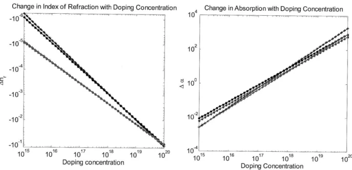
To obtain these results, Soref et al. compiled, from the literature, measured values of absorption, a, as a function of wavelength and doping. They then used the Kramers-Kronig relations to calculate the expected change in refractive index, and plotted these results along with the absorption data on a series of graphs. Interpolating, they came up with a set of data that relates free carrier concentration to Aa and to An in the two telecommunications bands (1.3 and
1.55um). Their results for 1550nm are shown in Figure 3. 10- -,- -auCO. Tz3COM 10 ~-I -FREE ELEC7TRDN3 MEE m4OL!FS 100:-'-100 REEE ELCZGNRDS / 10 3 10 10
I I I ill INJ I r ~ 10-l - 11,11 11jI
to' 10s j019 101 1017 1018 10 1020 101 __V SILICON T - ILO' 100 /
7
-N 10 10 10 102c AN (crn- 3) Figure 3 Left to right: fits to the change in refractive index as the concentration of electrons and holes varies (Soref et al. Fig. 11), the change in absorption coefficient with a change in free electron concentration(Soref et al. Fig. 14), and the change in absorption coefficient with a change in free hole concentration (Soref et al. Fig.15). From [10].The data can be fit to get simple equations relating these quantities. These equations are usually given as [1], [6]:
An = -8.8e-22-ANe -8.5e-18-(ANh) 0 8, and Aa = 8.5e-18-(ANe) + 6.0e-18-(ANh)
However, refitting Soref et.al.'s absorption data shows that a better fit is actually given by
[5]:
Aa = 9.1e-22-(ANe)1.2 2 + 2.5e-20-(ANh)'. 13
It is useful to note that neither of these sets of equations is presented in Soref et. al.'s original paper, though the first set of equations is used in later papers by Soref (for example, [11]). Soref et. al. did do a similar fit to the data in their original paper, but ended up with slightly different numbers, which are not, generally, used in the literature.
Index changes caused by carrier changes can be as high as 2x10⁻³ for 1x10¹⁸ p-type doping in
silicon. Modulation speeds, which are determined by the time necessary to move the free carriers, can be in the GHz range [5]. Thus, the plasma-dispersion effect is the most widely used modulation mechanism in the current silicon modulator literature. It is this mechanism that is used for all the designs in this thesis.
Mach-Zehnder Modulators - Rational and Transfer Function
There are many different device designs for exploiting a change in index to create a working modulator. Possibly the biggest split in these structures is between resonant and non-resonant modulators. Resonant modulators are usually made in rings or photonic crystal cavities [5] [20]
[18]. Non-resonant modulators are usually made in a Mach-Zehnder (MZ) configuration.
Resonant modulators have a smaller footprint and require less power, but have smaller bandwidth and are more sensitive to temperature and fabrication variations. Mach-Zehnder modulators require more power and space, but have larger bandwidth and are more robust to variations [2]. Because the relevant application requires a large bandwidth, this work addresses Mach-Zehnder modulators
A Mach-Zehnder (MZ) modulator is created by splitting the power from an incoming light
pulse between two paths of different effective length, then recombining it at the output. When the pulse recombines, the difference in effective length has caused a phase difference, which yields either constructive or destructive interference, thereby changing the output amplitude. In
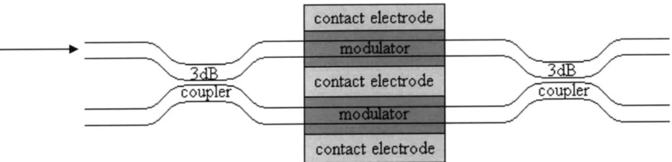
order to dynamically change the output signal, it is necessary to dynamically change the effective length of one or both arms. Such a change is accomplished by including a device which employs one of the phase-affecting modulation effects described above: in our case the plasma-dispersion effect. For the remainder of this work "MZ modulator" will refer to the entire modulator structure, while "modulator" or "phase-shifter" will refer to the device present in one or both arms to modulate the effective path length. In order to ensure that full modulation depth can be achieved-that is that full cancelation is possible when the arms are 180* out of phase-the light must be split evenly between the two arms. This can be accomplished with either a 3dB coupler or a Y-junction. In our system (depicted in Figure 4) 3dB couplers are used as the 50-50 splitter at both the input and the output.
Modulators are included in both MZ arms of our system [7]. While, technically, only one arm needs to contain a phase shift (and thus a modulator), operating in both arms allows for push-pull operation. In push-pull, opposite biases are applied to the arms around some DC bias point, adding more phase in one arm and less in the other. A ir-phase change can then be achieved in half the modulator length. To take advantage of the most linear part of the MZ transfer function, the MZ modulator is operated in quadrature. To place the MZ modulator in quadrature, a titanium heater is fabricated over one of the modulator arms. The heater is then used to adjust the accumulated phase change using the thermo-optic effect (see above) until the outputs indicate that the device is in quadrature [7]. After the second 3 dB coupler the desired output (the optical version of the input electrical RF signal) is transmitted in the top waveguide and its complement in the bottom one. Often both outputs are used in future processing to minimize errors [7].
Fehld3 dB
couple
The MZ transfer function itself can be calculated as follows. It is assumed that all light is input on the upper channel, that the MZ modulator is operated at quadrature in push-pull, and that the 3dB input and output couplers are ideal. The phase shift on the upper arm is denoted by eip and that on the lower arm by (P2 and the input power is denoted by Po. The requirement that the MZ modulator be operated in quadrature places an extra 7n/2 phase-shift on one of the arms. In this calculation it is placed on the lower arm. For simplicity it is assumed that the modulators are lossless. The effects of loss will be discussed in the "Linearization of MZ Modulators" section below. After the first 3dB coupler the amplitude in the upper arm is given by
At1 1 P7 2 and that on the lower arm by:
Ab = Pe'e'22 /
The heater and the modulators add a phase change to these signals:
At2 ~ P (I/
b= VPOeiT1/ 2
At the second 3dB coupler part of the light in each arm stays in that arm and part is coupled across to the opposite arm. The final output amplitudes are :
t3
e
2+ir/2 2 4 sin 192
b3 - P el2+1fIrr/
rr
2 2 42 4)2 4)
Multiplying by the complex conjugates yields the final output powers:
P,,, =P sin2 (91 -92 _
It can be seen that the two outputs are complementary, and that the MZ transfer function is sinusoidal, and not linear, in shape. This has important implications for modulator accuracy which will be discussed in "Linearization of MZ Modulators" section below.
Figures of Merit
There are several common figures of merit (FOM) that are used when evaluating modulator performance. The most important ones are V,,L, the 3dB optical bandwidth, the 3dB RF bandwidth, and the insertion losses incurred by the device. These last three are more or less
self-explanatory. The 3dB optical bandwidth is the wavelength range over which the device works. The 3dB RF bandwidth is the fastest electrical signal that can be faithfully modulated. The insertion loss is the total optical loss through the device, including all waveguide loss mechanisms and input and output coupling. It is usually given in dB/cm, and, especially in smaller devices, can be quite high [26]. V2L is meant to be a measure of device sensitivity and corresponds to the length of the device times the voltage which, when placed across it, yields a i-phase-shift (thus allowing the MZ output in one channel to be changed across the full range from zero to the input power using a phase-shift section in only one arm). In linear, electro-optic modulators (like LiNbO3), VTL is a very good metric; increases in device length translate to
decreases in voltage in such a way that the VL of a given modulation scheme stays constant even as device length varies. However, in silicon plasma dispersion modulators, this FOM is problematic because such a nice relationship does not hold. More specifically, because the carrier concentrations are not linear functions of bias voltage, some voltage steps create larger changes in phase than others. The DC operating point and the amplitude of the RF voltage swing, thus, both matter when determining the phase change achieved. There are then locations on this phase-change versus voltage curve where increasing the voltage has more or less effect than increasing the length. For example, in a forward biased diode modulator, the relationship between voltage and phase is exponential and a small change in voltage can swamp even a large change in length [5]. Alternatively, in a reverse biased diode modulator, once the waveguide is largely depleted, increasing the voltage across the device does little in comparison to increasing the device length. Because, in the end, the quantity of interest is the power required to operate the device, a much better FOM would simply be the total RF power required to achieve a a-phase-shift. The footprint of the device, which is more relevant than the length in determining packing density, could then be reported separately
Fundamental Limitations of Plasma-Dispersion MZ Modulators
The plasma dispersion effect relies on injection or extraction of free carriers in order to create a change in refractive index. In order for a modulator based on the plasma dispersion effect to
work, there must exist both a way of injecting and extracting carriers at high speed, and a way to exploit the generated change in refractive index to create modulation.
The generation of free carriers is usually accomplished though the inclusion in the design of one or more electronic devices which inject or deplete them. Diodes are by far the most common structures used in the literature [5] [4] [1] [19] [20]. MOS capacitors are also common [9] [14]
[15] [16] and a few researchers have used specialty structures (e.g. [12] [13] [2] [37].) In
non-integratable modulator designs carrier creation is sometimes accomplished by use of an external light source (such as a pumping laser) [17]. The work in this thesis focuses on diode structures, with some work on MOS capacitors.
The details of diode and MOS capacitor modulator structures are discussed below. However, it is first useful to consider the limitations imposed by the use of the plasma dispersion effect itself.
The first restriction to note is that changes in refractive index are coupled with changes in the loss. This is always the case - refractive index and loss are related through the Kramers-Kronig relations. In the case of the plasma dispersion effect, it is clear what the physical source of much of this loss is: free carriers can be excited optically within the bands and then relax back thermally through the emission of one or more phonons [6]. The more free carriers there are, the more undergo this process, and the higher the loss is. Because a certain amount of index change is associated with the presence (at some point) of a given number of carriers, it will also be associated with a minimum amount of loss. In general, holes yield both a larger change in index and a lower loss. It is therefore desirable that phase changes be accomplished entirely using holes. While this is not possible in practice (though it is possible to mainly use holes), to discuss fundamental limitations it will be assumed for the remainder of this section that all free carriers are holes.
Given the maximum tolerable loss in a silicon phase-shifter that uses the plasma dispersion effect, the maximum achievable phase change can be calculated by first assuming that all losses in the waveguide are the result of free carriers (with no contributions from side-wall roughness, insertion loss, etc.) It is further assumed that the dependence of the index of refraction change on free carriers has the form:
and that of loss on carriers has the form:
Aa = A,(Ap)p"
Where Ap denotes the change in the hole concentration and An, Aa,pn, andpa are coefficients. The maximum phase shift achievable for a given amount of loss, Mss, is then:
A ~p = k LC , An 1 1 I (
) l
LC, A,
where L is the length of the phase shifter, Cf represents how much of the mode is confined in the region of carrier change, and M10s is the total loss, in dB, tolerated through the device. From this equation we note that if pa pn the achievable phase shift will be a function of device length and of confinement factor. Because these coefficients are, in fact, not the same for holes in silicon at
1550 nm, we can see that a confinement factor of one (the highest allowed) will yield the most
phase shift, and that longer modulators with lower carrier densities will achieve larger phase shifts per loss than shorter ones with higher carrier densities. Specifically, at 1550 nm the above equation becomes:
Ap=k0LCf *-8.5e-18 M10 1 0>n(1O)j
6.Oe-18-LC,
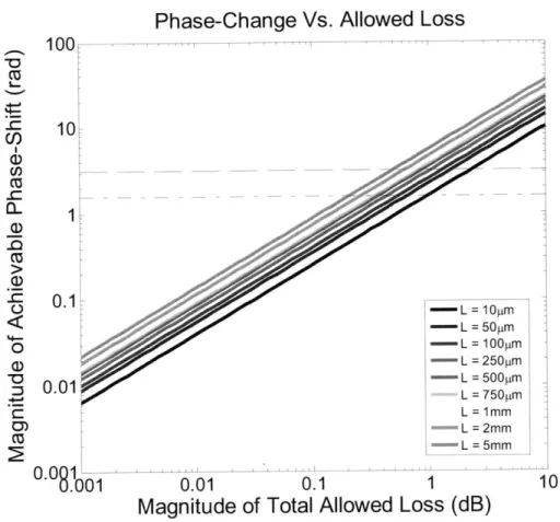
Phase-Change Vs. Allowed Loss
(U -C al) --0a)
0) a) 3; 100 10 1 0.1 0.010.
0
01o
0.001
0.01 0.1 1Magnitude of Total Allowed Loss (dB)
Figure 5: Dashed line corresponds to a n shift, dashed-dotted line to a n/2 shift. In a push-pull MZ modulator a n/2 shift in each arm is enough to achieve full modulation depth.
The 7r/2 radian shift needed to achieve maximum modulation depth in a MZ modulator driven
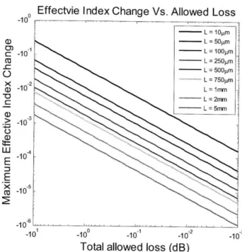
in push-pull, is theoretically achievable for all considered lengths at a total loss of less than 1 dB. However, almost three times as much phase shift is achievable in the longest device. To see why such a difference is present, it is useful to consider carrier concentration and the effective index change as a function of the total losses. These are shown in Figure 6.
Carrier Concentration Vs. Allowed Loss
Total allowed loss (dB)
Allowed Loss per Distance
-10 -10 -10 -10-2
Total allowed loss (dB)
Figure 6: (a) The maximum carrier concentration that can be present for a given loss and 100% mode confinement. We can see that
short modulators have significantly higher
changes in carrier density than longer ones. (b) The maximum index change possible per length in the material at the desired loss/length value, (c) The maximum loss/length value given the maximum tolerable overall loss.
102
10~4
-10 -10 -10- -102 -10-3
Total allowed loss (dB)
It can be seen that in the shorter structures, higher carrier concentrations are used to make up for the shorter length. However, because loss increases at a faster rate with carrier concentration than index change does, these higher concentrations are not able to compensate completely for the length difference. In the case where the loss and index change relations are of the same order, as is the case for electrons, increasing the carrier concentration while shortening the length leaves the overall phase shift unchanged.
The above calculations represent a theoretical limit and are, of course, unrealistically optimistic. The modal confinement to a modulated carrier region is usually much less than 50%, not the 100% assumed here. Furthermore, the modulated region, and thus the confinement to it, changes in volume as device doping concentrations are changed. Often, though not always, higher doping concentrations yield poorer overlaps, preventing the full benefit of having more carriers present from being realized. Making longer devices is also problematic, as not only is small size a desired modulator property, but there are often other losses (such as those from sidewall roughness or impurities) that limit practical device length.
Fundamental limitations to device speed also result from the use of the plasma dispersion effect. Because the index change is caused by a change in carrier concentration, it is necessary to move carriers into and out of some region of space. The speed that these carriers can be moved will determine how fast the device can be operated. There are several physical mechanisms that can limit speed. In the case of minority carrier presence, these carriers must either travel out of the region or recombine. Since both diffusion and recombination are slow processes, clearing a volume of minority carriers can take on the order of 100ps-lps and can place a severe limit on device speed - limiting performance to a few GHz at best. However, as modulation can be accomplished with majority instead of minority carriers, lifetimes do not provide a fundamental limit on device speed.
When only majority carriers are present, speed is usually limited by the dielectric relaxation rate of silicon, the RC time constant of the device, or by the saturation velocity of the carriers. The dielectric relaxation time is a measure of how fast a perturbation in the distribution of majority carriers can recover to the equilibrium distribution. It is a function of doping and is generally well known (it is given by F/). In p-doped silicon, with NA = lx1018 cm-3, the dielectric relaxation time is around 4x 10⁻⁴ s, which, if dominant, would allow the device to
operate at about 30 THz. The RC time constant places a speed-limit based on the capacitance of the device. While, in practice, this is often the limiting factor, there is no theoretical reason why it needs to be. Presumably, a low-capacitance, low-resistance design could be realized by either good device engineering (particularly if holes and electrons could be made to move in the same direction making the carrier plasma charge neutral and, thus, capacitance free), by the use of traveling wave electrodes to cut capacitance, or even, for some device designs, simply if the contacts have low enough capacitance and resistance that the intrinsic RC time constant of the
device (which can be quite low) dominates. It is, therefore, assumed that the RC time constant does not limit device performance. However, carriers cannot move arbitrarily fast - moving carriers scatter off the vibrations of the silicon lattice, not matter how pure the material, how high the field, or how few other carriers are present; the resulting limit on their speed is known as the saturation velocity. In situations where carriers need to move across large distances to restore equilibrium, saturation velocity ultimately provides the theoretical limit to device performance. In silicon, the saturation velocity for electrons is 1x107 cm/s (or 1/1000 the speed of light). If the modulated region they need to move in and out of is 400 nm wide, device operation is then limited to 95 GHz. For holes it is 6x 106 cm/s. For the same modulated region width the device operation would then be limited to 57 GHz [1]. In general, if the distance the carriers must move is known, the maximum device speed can be determined from:
fAdB 2.4 where r =
-/ Vsat
where W is the distance the carriers must move and vsat is the saturation velocity [1]. Note that the distance that needs to be moved might not be the length of the guide. Particularly for movement of majority carriers in an accumulation layer or movement of the depletion region edge in a highly doped material this distance might be quite short. However, for other situations, such as large depletion width changes, a longer distance must be used. Again, saturation speed represents best case performance. Usually, device speed is limited to much lower values by the RC time constant.
One final consideration is the limit on optical bandwidth from the plasma dispersion effect. Although there is a limit placed on the optical bandwidth usable at a given speed from the wavelength dependence of Soref's equations, this usually is dominated in the MZ case by the wavelength dependence of the waveguide propagation constants and, more importantly, of the couplers into and out of the phase shifting sections. In general, the optical bandwidth usable in a given phase-shifter design will depend on waveguide geometry and system tolerances.
MODULATOR MODELING
Accurate modulator modeling involves modeling both the electronic carrier responses of the device to an applied bias and the optical responses of the modes to those carrier changes. The modeling work in this thesis was split into two different parts. First, an electronic structure was designed and the carrier distributions were calculated either analytically or using Synopsys's SentaurusTM TCAD software suite. Then, those carrier distributions were imported into MATLABTM and used to calculate the optical response of the device. The work in this thesis focused on the design of the phase shifting modulator sections. Design of the overall MZ modulator structure, including couplers, was not undertaken. However, some analysis of the impact of the phase shifting section design on overall MZ performance was undertaken in the
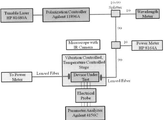
section entitled "Linear Modulators" below.
Electrical simulations were carried out using both analytic models and full scale simulations. Full scale electrical simulations were implemented in Synopsis's SentaurusTM software suite. Optical simulations for straight and rib waveguides were performed in MATLABT M, where a
mode solver previously developed by Milos Popovic was used to calculate effective indices and losses. Because Sentaurus does not output directly to a MATLAB-compatible format it was necessary to parse the output files into a readable form. It was also necessary to re-grid the carrier distributions from the finite element grid used in Sentaurus to an evenly spaced finite difference grid for input into Dr. Popovic's mode solver (MMS). The overall simulation flow for these files is outlined in Figure 7.
Optical simulations for photonic crystal waveguides were carried out using the MIT Photonic Bands software suite developed by Steven Johnson's group, the output of which was analyzed in MATLAB and in MayaViTM.
D @vica Structure is created
V =0
Carrier Concentration s (electrons and holes) are found at desired output voltages
Device Structure is meshed
Paramters are set and device simulat ion is run
V= 0 V = 0
_110
Carrier Conceniration is converted to a rectangular gid in
MATLAB
Effective Index Change and Absorption are found as afunction of biasvoltage
Index Panes are created
Ii
Optical Modes are calculated and optical parameters found
Figure 7: Flow diagram of simulation process
Electrical Simulation Details
Electrical simulations were carried out using both Sentaurus Structure Editor and Sentaurus Device. The accompanying Synopsys plotting software, Tecplot, was used in the processing of the output files. Sentaurus Workbench, a wrapper program, was used to organize the larger runs.
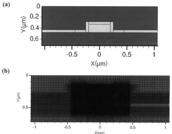
Device structures were created and meshed using Sentaurus Structure Editor. To create a device structure, a Scheme script placing material blocks, doping profiles, and contacts was written (see appendix B). For large parameter sweeps, Sentaurus Workbench was used to vary the desired input variables without the need to hand code each desired structure. To simplify device creation and analysis all doping profiles were assumed to be constant and abrupt. The boundary geometry specified for the device was then meshed using a Delaunay meshing algorithm suitable for finite element simulations [46]. A fine mesh was used in areas of particular interest, such as diode junctions. The mesh was allowed to expand away from these areas. An example boundary file and mesh (expanded for illustration) are shown in Figure 8. To keep simulation times down, the mesh was made as large as possible while still maintaining the desired accuracy. This accuracy varied from simulation to simulation: with the least accuracy demanded for original exploratory simulations and the most for rigorous optimization simulations.
(a)
0
0.2-
0.4-
0.6--0.5
0
0.5
1
X(pm)
(b)
0.5--1 -0.5 0 0.5 X(pm)Figure 8: (a) Boundary geometry of example device structure, (b) Example Delaunay simulation mesh. Mesh is
After the device structure was created and meshed, its electrical performance was simulated using Sentaurus Device (Sdevice). In Sdevice, the Poisson equation and the electron and hole continuity equations were simultaneously solved. In many simulations, the heating equation was also solved. However, for most devices of interest (reverse biased diodes and MOS capacitors) its inclusion did not have a significant impact on simulation results.
A number of physical and numerical parameters can be set from the command and parameter
files of an Sdevice simulation. A few of the more important ones will be highlighted here. (For an example command file, see Appendix B). Because of the high doping levels used in parts of the modulator, it was necessary to force the use of the more accurate Fermi statistics over the computationally more efficient Boltzmann statistics when calculating carrier densities. This was done by specifying the keyword "Fermi" in the physics section of the file. By default the mobility is a function of temperature only; this is not physically correct. Mobility degradation due to doping, high electric fields, and proximity to surfaces was added into this model. Similarly, all recombination mechanisms need to be explicitly specified: Shockley-Read-Hall (SRH), surface and Auger recombination were included. Avalanche and band to band generation were also incorporated into many simulations. Doping dependence was included in the SRH calculations. In all silicon simulations, the carrier lifetimes were left at the accepted values of 10 ps for electrons and 3 ps for holes, which are also the defaults. To find the surface recombination velocity at the silicon-SiO2 interfaces, simulation results were fit to previous simulations that were fit to measurements of forward biased diode performance for diodes fabricated at Lincoln Laboratory. The resulting surface recombination velocity was 2x105 cm/s. This value is important in minority carrier dominated situations, as surface recombination is the dominant recombination process for minority carriers in silicon devices of this size. Using this surface recombination velocity the overall minority carrier lifetime was found to be around 1 ns. Devices whose responses are characterized mainly by majority carrier dynamics are not sensitive to this value. In forward bias diode simulations that involved polysilicon, the surface recombination was turned off, and the carrier lifetime in the SRH model varied by hand in the
100 ps-10 ns range. This was to account for the fact that the large number of flaw and trap states
present in polysilicon dominate the lifetime. Because the number and type of these flaw and trap states depends heavily on the specifics of the device processing, predicting the lifetime values beforehand is impractical. Instead, this lifetime range was considered and devices designed that
could work throughout it. A list of important physical parameters input to simulations can be found in Appendix A.
Optical Simulation Details
As stated above, Sentaurus does not output its results in a MATLAB readable format. It was, thus, necessary to first convert the output files from ".tdr" format to Tecplot's ".dat" format and then to parse them into a usable array. Because the optical mode solver needs a rectangular grid, and Sentaurus simulations use a finite element grid, it is necessary to re-grid the electrical output before it is input into the mode solver. It is also necessary to convert the calculated carrier distributions into index and absorption distributions.
Each output file corresponds to a specific structure at a specific voltage. To re-grid these files, the location of and the variable values at each grid point are placed into a list and exported in ASCII form. A rectangular grid of blocks of the desired size (usually 2 nm x 2 nm) is created in MATLAB and the finite element grid locations in the list are placed onto this new grid. If more than one location falls within the same grid square, the values are averaged. To fill in
squares in which no grid points fall, a linear interpolation scheme is used.
Once the rectangular grid is created, it is necessary to prepare the electrical output for input into the MMS. The complex refractive index at each point is determined according to
;1(x, y9,)= no (x, y,)+ An(x, y,A)+ i Aa(x, y, A)/2ko
where no is the material index of refraction, and An and Ja are, respectively, the change in index of refraction and absorption due to carriers, and are calculated using Sorefs equations. At 1550nm, the standard equations from Soref presented above (in the section entitled "Plasma-Dispersion Effect") are used. However, there are no such standard equations at other wavelengths. Soref's original paper does contain graphs (but not equations) that relate change in refractive index and absorption to carrier density at a variety of wavelengths. An interpolation program based off data read from these graphs was implemented by Eugen Zgraggen, a visitor to Rajeev Ram's group, and is used here when results at wavelengths other than 1550 nm are desired. Because this program yields slightly different results at 1550 nm than the standard form of Sorefs equations (see Figure 9), the results at 1550 nm are recalculated using this interpolation program when comparisons across wavelengths are desired (for, say, optical bandwidth calculations) to ensure consistency. However, in order to facilitate comparisons to
the literature and to previous results in the group, when only 1550 nm wavelength results are wanted, the standard form of Soref's equations is used.
Change in Index of Refraction with Doping Concentration 4 Change in Absorption with Doping Concentration
-1 0_ 10 -10 102 -10-10 -10 1 -102 10 -10 -10 _________1_______ _________4_______ 105 1016 1017 1018 1019 1020 10 015 1016 117 1018 1019 10
Doping concentration Doping Concentration
Figure 9: Comparison of change in index and absorption with carrier concentration at k=1550 nm as given by the accepted forms of Sorefs equations (circles) and the program from E.Zgraggen, which interpolates from Sorefs
graphs (crosses). Green lines indicate changes with hole concentrations and black lines those with electron
concentration. As can be seen, there is good agreement in the area of 1 x10¹⁸ carriers per cubic cm, but progressively
less agreement further away from this range. At the edges of the graph (concentrations of 1 X10 1 5cx0m3 or 1 x 10² 0cm-3)
values may be off by a factor of two or more. Agreement is much better for index variations than for absorption variations.
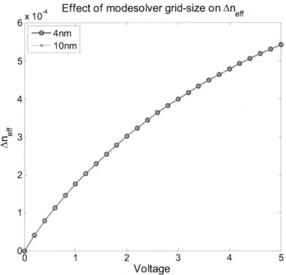
After the carrier distributions are converted into a complex index distribution, that index distribution must be averaged for input into the mode solver. This is necessary because the mode solver uses an iterative Arnoldi algorithm and abrupt changes in matrix values hurt convergence and accuracy. Due to time and memory constraints, the size of the grid input into MMS is often coarser than the newly created grid of the Sentaurus outputs. If the two grids use different x- or
y- direction steps, the complex index distribution is first re-gridded onto the MMS grid. Changes
in MMS grid size below 10 nm x 10 nm grid squares seem to have little impact on results (see Figure 10). Furthermore, because the computational domain for Sentaurus electrical simulations usually does not extend much beyond the silicon regions (while the modes can), extra oxide padding is added around the Sentaurus computational domain region to ensure that no problems are caused by computational domain boundaries. Once this is done, standard area-arithmetic index averaging is applied. The averaged index distribution is then passes to MMS where the
eigenvalues and eigenvectors of the index distribution are found using an Arnoldi algorithm in shift-invert mode, and the complex electric and magnetic fields along with the complex propagation constant are returned.
10
-4 Effect of modesolver grid-size on AneffVoltage
Figure 10: Below 10 nm x 10 nm grid squares, x- and y-direction step size of the grid input into MMS has little
impact on results. Here the index change calculated for an example modulator design is shown for both a 10 nm x
RIB WAVEGUIDE MZ MODULATOR DESIGNS
A common waveguide design for modulator structures is the rib or ridge waveguide, pictured
in Figure 11. This structure is popular because light is guided in and confined by the rib region, while the slab allows electrical contact to be made to an intrinsic device in such a way that the highly-doped and metal contact regions are kept separate (or largely separate) from the optical mode, thus, limiting losses to acceptable values.
Contact \ode Contact
Rib
}Slab
lef ;Figure 11: (a) A standard Rib-waveguide consists of a slab section with a rib placed on top, (b) the rib serves to confine the mode away from the ends of the slab, allowing lossy metal contacts to be placed there and successful electrical contact to be made to the intrinsic modulator device.
When designing a rib waveguide, there are two main design spaces: that of the electrical device and that of the optical waveguide. The key is to achieve regions of high index modulation from the electrical device and to integrate the two such that the optical mode has maximal overlap with the area of the device that sees index modulation.
Modal Overlap Considerations
Overlap between the mode and the modulated region is, of course, important in all modulator structures. It will be explored here in the context of the plasma dispersion effect in rib waveguides. Because only part of a mode is carried in the modulated, or active, region of the waveguide, it is necessary to calculate an effective index change from the refractive index change present in the active region. The effective index change reflects the actual change in phase accumulated by a mode traveling through the waveguide. When refractive index changes are small enough to be considered perturbations (that is the mode shape does not change noticeably), the effective index change can be calculated as the change in refractive index of the region times the confinement factor of the mode to the region. What percentage of the mode experiences what index change depends significantly on both the size and location of the active region and on the geometry of the waveguide itself.
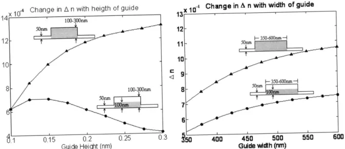
The two graphs in Figure 12 show the effect of waveguide geometry on effective index change. The height and width of the rib in a rib waveguide are varied and the effective index of a plain silicon guide with the given geometry is compared to that of a perturbed guide. Two perturbations are considered. In the first, the perturbed region covers the bottom 100 nm of the guide. In the second, it covers the whole guide. Because the mode is more confined in a larger waveguide, when the perturbation occurs throughout the waveguide, the effective index change simply increases as the size of the guide increases and there is no optimal value for either dimension. However, when the active region only covers a portion of the waveguide, there can exist optimal values for waveguide dimensions. Here, the 100 nm profile is constant over the width of the guide, but varies in height. Therefore, there is no optimal width - wider is always better as it pulls more and more of the mode into the guide and into the perturbed region - but there is an optimal height. The maximum in effective index change with height reflects the trade-off between obtaining the best overlap between the peak of the mode and the active region and maintaining high overall confinement of the mode in the guide thereby keeping the modal peak high. Too short, and there isn't enough light in the waveguide to get optimal modulation even when the modal maximum is in the active region. Too high, and the modal peak moves higher in the guide leaving only the mode's edges to see the index change present in the bottom. Were the region of refractive index change to be a vertical strip instead of a horizontal one, there would be no optimal height, but there would be an optimal width.
Change in A n with heigth of guide
0.1 0.15 0.2 0.25 0.3 '50 400 450 500 550 600
Guide Height (nm) Guide width (nm)
Figure 12 (a) Change in effective index (from the plain, unperturbed silicon waveguide case) with height when an index perturbation equivalent to the injection of 5x 10¹⁷ holes is applied across the bottom 100 nm of the waveguide (circles) and across the whole waveguide (triangles). The rib width is fixed at 500 nm with a slab height of 50 nm surrounded by SiO2. Guide height reflects the entire height of the center of the guide (from the
SiO2 substrate to the top SiO2 cladding). Note that, for a 100 nm perturbation there is a maximum An, while for
perturbation of the whole waveguide, An increases continuously with height. (b) Change in effective index under the same index perturbations as a function of guide width. Here the guide height was held constant at 150 nm. In both cases effective index change simply increases with width.
Within a particular waveguide design, the details of the perturbation layer location and strength obviously also have a large impact on the mode. The three graphs below demonstrate this impact on effective index given a specific waveguide geometry. In the first graph, a 50 nm layer of refractive index change is moved from the bottom to the top of the waveguide. An analogous situation in an actual device would be moving the vertical location of a junction. In the second graph, the size of the index perturbation in a 100 nm layer at the bottom of a waveguide is varied. Changing doping levels to cause more or less carrier injection or depletion would cause the same type of difference in a real structure. Finally, the third graph shows how effective index change changes as the active region is increased to cover the whole guide. Increasing bias voltage to affect a larger device area would accomplish the same thing in an actual device.
Looking at the first graph, it should be noted that the index perturbation has a clear peak. Because the mode is concentrated in the center of the guide, as the layer of refractive index change approaches this region, the effective index change increases, and as it moves away it decreases. The difference in effective index change between the location of maximum overlap and that of minimum overlap is greater than 30%. Clearly the location of the junction relative to the modal maximum is important. The slope of the third graph also illustrates this point. Here,