HAL Id: hal-02530804
https://hal.archives-ouvertes.fr/hal-02530804
Submitted on 3 Dec 2020
HAL is a multi-disciplinary open access
archive for the deposit and dissemination of
sci-entific research documents, whether they are
pub-lished or not. The documents may come from
teaching and research institutions in France or
abroad, or from public or private research centers.
L’archive ouverte pluridisciplinaire HAL, est
destinée au dépôt et à la diffusion de documents
scientifiques de niveau recherche, publiés ou non,
émanant des établissements d’enseignement et de
recherche français ou étrangers, des laboratoires
publics ou privés.
Scanning the plasmonic properties of a nanohole array
with a single nanocrystal near-field probe
Thi Phuong Lien Ung, Rabeb Jazi, Julien Laverdant, Rémy Fulcrand, Gérard
Colas Des Francs, Jean-Pierre Hermier, Xavier Quélin, Stéphanie Buil
To cite this version:
Thi Phuong Lien Ung, Rabeb Jazi, Julien Laverdant, Rémy Fulcrand, Gérard Colas Des Francs,
et al.. Scanning the plasmonic properties of a nanohole array with a single nanocrystal near-field
probe. Nanophotonics, Walter de Gruyter, 2020, 9 (4), pp.793-801. �10.1515/nanoph-2019-0409�.
�hal-02530804�
Research article
Thi Phuong Lien Ung, Rabeb Jazi, Julien Laverdant, Remy Fulcrand, Gérard Colas des Francs,
Jean-Pierre Hermier, Xavier Quélin and Stéphanie Buil*
Scanning the plasmonic properties of a nanohole
array with a single nanocrystal near-field probe
https://doi.org/10.1515/nanoph-2019-0409
Received October 7, 2019; revised January 1, 2020; accepted January 26, 2020
Abstract: The electromagnetic properties of ordered hole
nanostructures in very thin metal films are character-ized using CdSe/CdS nanocrystals (NCs) as nanoprobes. The characterization of the local density of optical states (LDOS) on the nanostructure is possible by the measure-ment of their photoluminescence decay rate. Statistical measurements are performed in the far field to show the average increase of optical modes. A determinist approach using an active single NC nanoprobe in the near field gives access to a more precise characterization of the LDOS. The optical properties of the structure come from the coupling between localized surface plasmons created by the holes and surface plasmon polaritons. A strong concentration of optical modes is observed around the holes thanks to the active near-field nanoprobe. With different NC orientations, the strong influence of the com-ponent perpendicular to the surface in the very near field of the LDOS is observed. Finite differential time domain simulations of the different components of the electric field in the very near field of the structure confirm that the localization of the electric field around the holes is only due to the normal component as observed with the nanoprobe.
Keywords: near-field optics; plasmonics; nanoemitter.
1 Introduction
With the development of material science at the nanoscale, surface plasmons (SPs) offer very promising possibilities for transferring information through nano-structure surfaces [1]. At the core of optical properties of metals, SPs have opened up a wide range of applica-tions in modern photonic techniques, such as biomedical sensing [2, 3], light-matter interaction [4–6], or quantum information processing [7, 8]. SPs become attractive upon irradiation with light on low-dimensional nanostructures (two-dimension, 2D or one-dimension, 1D). They generate propagating surface plasmon polaritons (SPPs) or local-ized surface plasmons (LSPs) associated with electromag-netic field enhancements at the interface between a noble metal and a dielectric medium.
Among the great variety of 2D plasmonic structures, much attention has been paid to 2D periodic nanohole arrays which exhibit SPPs and LSPs. At the beginning of the last century, intensive works have been devoted to extraordinary optical transmission (EOT) through sub-wavelength hole arrays [9, 10]. The physical origin of the EOT is still in debate, but in the first approximation, it results from the coupling between the incident light and the SPPs of the nanohole arrays localized at the film interfaces [11–15]. Another explanation invokes dynamical light diffraction [16–19]. This EOT is observed when nano-metric holes are drilled in a thick metallic layer more than 100 nm.
When the thickness of metallic films gets close to the skin depth, an opposite effect was observed. Braun et al. reported that less light is transmitted through perforated structures in very thin gold films with a thickness of 20 nm [20]. The suppressed transmission in a periodically per-forated thin film was well explained by Spevak et al. by means of analytical and numerical calculations [21]. An extraordinary absorption up to 50% can be achieved. Similar to transmission in very thick metallic film, SP
*Corresponding author: Stéphanie Buil, Université Paris-Saclay,
UVSQ, CNRS, GEMaC, 78000 Versailles, France,
e-mail: stephanie.buil@uvsq.fr. https://orcid.org/0000-0003-3403-6258
Thi Phuong Lien Ung, Rabeb Jazi, Jean-Pierre Hermier and Xavier Quélin: Université Paris-Saclay, UVSQ, CNRS, GEMaC, 78000
Versailles, France
Julien Laverdant and Remy Fulcrand: Université de Lyon, Institut
Lumière Matière, Université Claude Bernard Lyon 1, CNRS, Université de Lyon, F-69622 Villeurbanne, France
Gérard Colas des Francs: Laboratoire Interdisciplinaire Carnot de
Bourgogne (ICB), UMR 6303 CNRS, Université Bourgogne Franche-Comté, 9 Avenue Savary, BP 47870, 21078 Dijon Cedex, France
Open Access. © 2020 Stéphanie Buil et al., published by De Gruyter. This work is licensed under the Creative Commons Attribution 4.0 Public License.
794 T.P.L. Ung et al.: Scanning the plasmonic properties of a nanohole array
excitation is considered as the origin of the resonance absorption energy. Even if less works have been devoted to ultrathin films compared to EOT, periodic nanohole arrays in very thin metal films has been investigated by several groups [22, 23].
In the case of ultrathin metallic films, the diffraction can be distinguished from the SP coupling effects. The study of a single hole represents a crucial first step. In 2007, Kall and co-workers performed successfully scanning near field optical microscope (SNOM) experiments to analyze in detail the LSP-SPP coupling in a single hole placed in a 20 nm gold film [24]. As a consequence, the experiments explain the presence of a dipolar LSP resonance mode in a single hole and the dominance of the SPP mode in the sur-rounding gold film. In the case of an array, the LSP of the holes couple together via the SPP of the gold film [25]. This coupling depends on the parameters of the array (size of the holes, period, and thickness of the layer) and can lead to optical modes localization.
A very efficient way to probe the electromagnetic mode distribution of a nanostructure is to study its cou-pling with nanoemitters. The spontaneous emission rate of the emitter is directly proportional to the local density of optical states (LDOS) at the emission frequency of the emitter [26]. In this article we propose to study the elec-tromagnetic mode localization via the study of the pho-toluminescence (PL) decays of CdSe/CdS nanocrystals (NCs). First, large fluctuations of the LDOS will be evi-denced with a confocal microscope before using a new kind of probe recently developed in the group and made of a single orientated NC at the end of a near-field probe. We will show that with this approach, crucial information about the localization and the nature of the optical modes can be obtained. Indeed, in this case it is possible to pre-cisely locate the nanoprobe on the nanostructure and to image the LDOS at a nanometer scale. Moreover, in this experiment, the dipolar orientation of the nanoprobe is determined making possible to get insight into the LDOS
in different directions in space. Previous studies reported the deterministic coupling of Nitrogen Vacancy centers or quantum dots using scanning probes or control nanopo-sitionning of the emitter in order to study the plasmonic properties of structures such as silver or gold nanowires, resonators, or pyramid antennas [27–32]. In all these studies the emission rate of the nanoemitter is measured at different positions as in our experiments. Even if the dipolar orientation is determined in one experiment with a nanodiamond probe, none of them deal with the partial LDOS. In this article, the measurements performed with this oriented NC nanoprobe will be compared to finite differential time domain (FDTD) simulations of the elec-tric field on the array showing interesting results on the behavior of the different components of the field.
2 Experimental methods
2.1 The nanohole array
The nanohole array was fabricated by a focus ion beam (FIB) technology (Zeiss NVision 40, Zeiss, Jena, Germany). First, a flat gold film is prepared by radio fre-quency sputtering under high vacuum conditions (10−9
Torr) on a glass substrate. The flat gold film has a thick-ness (t) of 38 nm with a roughthick-ness rms of 1 nm. Then the nanoholes are etched on this flat gold film with the FIB at high current with a precision of 1 nm. The hole array is fabricated in order to have a periodicity (p) of 425 nm and a hole diameter (d) of 100 nm (Figure 1). The absorption of this array is measured using a confocal microscope (IX 71, Olympus, Tokyo, Japan) illuminated by a white laser (SuperK EXTREME-white EXW-12, Birkerød, Denmark) and coupled to a spectrophotometer (Princeton Instru-ments-SP2750). The absorption is deduced from the reflection and the transmission measurements performed
on the array (Figure 2A). This measurement is compared to a numerical simulation (Lumerical software) using a FDTD method (Figure 2B) [33]. As we can see, the experi-mental result and the simulation are in good agreement. For comparison, the absorption of a flat gold film with the same thickness is shown. A strong enhancement of the absorption is observed. The absorption curves show two peaks at 620 and 750 nm with an absorption up to nearly 40%. This strong absorption is linked to plasmons and the array was tuned so that the first peak position matches the NCs emission wavelength. It has been dem-onstrated that plasmon resonances arise from the cou-pling between LSP mediated by SPPs of the film [25].
2.2 The nanoprobes
The CdSe/CdS core-shell NCs are synthesized by the decomposition of organometallic precursors with a small size dispersion (about 5%). The NCs have a diameter of 15 nm including a 3 nm CdSe core and a 6 nm CdS shell. Previous experiments have demonstrated that, due to this thick shell, the fluorescence of the NCs is not quenched on gold film [34]. Their emission wavelength is centered around 620 nm with a 30 nm full width at half maximum at room temperature and their fluorescence corresponds to the emission of two incoherent dipoles perpendicular to the crystalline c-axis [35]. The emission wavelength corresponds to the first absorption resonance peak of the hole array. This means that the fluorescence of the NC will couple to the plasmons of the film. The modification of the NC emission on the array will then depend on the electro-magnetic modes associated with the plasmon resonance.
2.3 Experimental set-up
The modification of the NC emission coupled to the nano-hole array will be studied with two set-up. The first one is a confocal microscope used to characterize the field enhancements on the array compared to a flat gold film and the second one is a near-field set-up used for very local studies of the field on the array. The confocal micro-scope is an inverted micromicro-scope coupled to an avalanche photodiodes (MPD, time resolution of 50 ps). The optical excitation is provided by a fiber-coupled pulsed laser diode (Picoquant LDH D-C, pulse duration ~100 ps) emit-ting at 485 nm. In order to create only one e-h pair and to avoid as far as possible the contribution of multiexcitonic states, a low power excitation is used. NCs are directly deposited on the array by spin coating and the dilution is chosen in order to detect the emission of individuals NCs. Time-resolved experiments can be carried out on individual NCs.
The SNOM set-up is based on an inverted microscope coupled to a commercial SNOM head (NTMDT) (Figure 3). In this experiment, a single NC is attached at the end of the SNOM tip. Its fluorescence is collected through the SNOM fiber and sent to a TTi QL355 avalanche photodi-ode connected to two data acquisition cards (National Instruments PCI-6602 and PicoQuant TimeHarp200) that record the arrival time of the photons emitted by the NC. Its orientation at the end of the tip is determined by fluo-rescence lifetime measurements performed at different distance from a flat gold film. These measurements are compared to a modelization and allow to determine the orientation of the c-axis of the NC at the end of the tip.
1 0.5 0 1 0.5 A B Grating
Flat gold GratingFlat gold
0 500 600 700 Wavelength (nm) Wavelength (nm) Nor maliz ed intensity Nor maliz ed intensity 500 600 700
Figure 2: Absorption spectra of 15 × 15 ordered hole array with
p = 425 nm and d = 100 nm in thin gold film t = 38 nm. (A) Experiment and (B) simulation.
SNOM electronic Acquisition x-y-z piezo driver APD Laser (405 nm) CCD
Figure 3: Near-field approach by SNOM with one NC acting as an
796 T.P.L. Ung et al.: Scanning the plasmonic properties of a nanohole array
The method to catch the NC at the end of the SNOM tip and to measure its dipolar orientation has been described in a previous publication [36]. The tip is mounted on a tuning fork which is attached to a piezoelectric scanner in order to perform nanometric displacement in the three directions (x, y, z). In addition, the sample holder is con-nected to a second piezoelectric scanner with two axes of translation (x, y) which allow the displacement of the sample in the horizontal plane. The NC is excited by a pulsed diode (LDH-D-C-405, PicoQuant, Berlin, Germany, pulse duration ~100 ps) emitting at 405 nm with a repeti-tion rate of 5 MHz. The NC can then be precisely placed at different positions (x, y, z) on the array.
3 Results and discussion
When a NC is placed over the array, its decay rate is modi-fied following the expression:
2 0 | |p p( , )r πω Γ ρ ω ε = (1)
where p is the transition dipole between two electronic states and ( , )ρp r ω is the partial LDOS projected along the dipole transition moment .p The decay rate of the NC
then depends on the number of electromagnetic modes at its position and on its orientation over the surface. In the experiments PL lifetimes which are directly related to the decay rate by the relation Γ = 1/τ are measured. To get an idea of the electromagnetic intensity on the surface, which is linked to the mode distribution, FDTD simulations of the near electric field were performed.
In these simulations, the illumination is made with a polarized plane wave at 620 nm. At this wavelength that matches the wavelength of the NC fluorescence, a high enhancement of the electric field around the nanoholes is observed, as we can see in Figure 4A that shows the inten-sity of the total electric field 10 nm above the surface. Even if these simulations cannot be strictly compared to the LDOS which would have needed a point-like illumina-tion with the integraillumina-tion of the dipolar orientaillumina-tion over the whole space, these high fields suggest a high mode concentration around the holes. A strong acceleration of the NC PL decay can then be expected on the array and if we look deeper, the decay rate of the NCs located around the nanoholes should be higher than on the other parts of the array. In the experiments that will be presented in this article, we will directly present the Purcell factors which are the ratio between the decay rate Γ on the film and the decay rate Γ0 on a glass cover-slip deduced from PL decay rate measurements.
3.1 Far-field approach
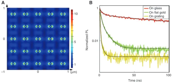
In these experiments, to account of the global effect of the array, a first statistical approach is performed with the confocal microscope described in section experi-mental set-up. To estimate the effect of the array, Purcell factors of a large number of individual NCs on the array are compared to the ones on a flat gold film with the same thickness. Typical fluorescence decays on glass, on flat gold, and on the array are presented in Figure 4B. These decays are always fitted by two exponentials, the longer component corresponding to the excitonic
10 1 0.01 A B 0 50 On glass On flat gold On grating 100 Time (ns) Nor maliz ed PL 5 1 (µm) 1 0 –1 0 1
Figure 4: A high enhancement of the electric field around the nanoholes is observed.
(A) Distribution of electric field 10 nm above the surface on the ordered hole array simulated by finite differential time domain (FDTD) and (B) PL decays of NCs deposited on different environments: glass, flat gold, and ordered hole array.
recombination and the shorter one to the trion recom-bination. All the Purcell factors are calculated with the long lifetime components. On the glass, a mean value of 60 ns is found and is used as Γ0 for Purcell factor calcu-lations. A large number of individual NCs are analyzed on the array and on the flat gold film. These results are presented in Figure 5. A mean value of 16 for the Purcell factor is found on the array compared to 10 on the flat gold film. The number of electromagnetic modes avail-able on the surface at the plasmon resonance frequency is then higher than on a flat gold film. The high Purcell factors measured on the array are in agreement with the strong electric fields observed on the FDTD image. Never-theless, to observe the special shape of the mode locali-zation deduced from the FDTD images, a more precise approach with a fine positioning of the NC is needed. For this reason, we developed a near-field nanoprobe with a single NC at its end as presented in the experimental set-up section. In the next section, the results obtained with this nanoprobe are reported.
3.2 Near-field approach
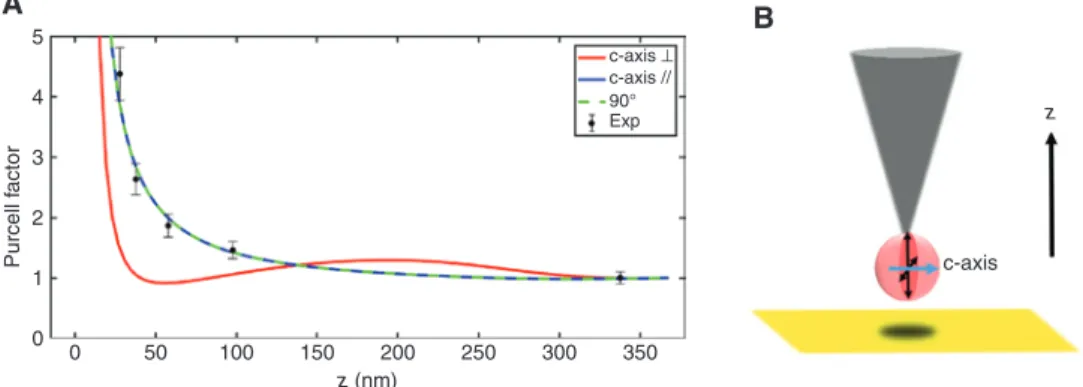
In this experiment, the decay rate of the single NC attached at the end of the SNOM tip is measured. As already men-tioned, the NC corresponds to a 2D degenerate dipole per-pendicular to the c-axis of the NC. Then, due to this dipolar orientation its emission will be sensitive to the LDOS pro-jected along its dipole transition moments and then its decay rate will depend on its orientation at the end of the tip. To confirm this effect, experiments in the near field have been carried out with two active tips. Two different NCs have been attached at the end of two tips to perform near-field experiments. These two nanoprobes are pre-sented in Figures 6 and 7. Their dipolar orientation is deter-mined by Purcell factor measurements on the flat gold part of the sample as described in Ref. [35]. Briefly, the modifica-tion of the NC emission lifetime is first measured as a func-tion of the NC gold mirror distance. The Purcell factor is then adjusted considering the NC orientation as a free para-meter. For the first one (NC1), the c-axis is found parallel to the surface. In this case, the 2D degenerate dipole can be described with one component perpendicular to the surface and the other one parallel to the surface. For the second one (NC2), an angle of 23° is found between the c-axis and the vertical axis. Compared to the NC1, the component of the 2D dipole along z axis is weaker. Once the measurements of the NC orientation have been performed on the flat gold part of the sample, the tip is brought onto the array. The array is first quickly scanned in order to get a topographic image and then to be able to position the tip. In agreement with the FDTD simulation presented in Figure 4A, three typical positions with different electric field values are chosen, a position 1 in between holes, a position 2 inside a hole and the last one, the position 3 close to the edge of a hole, where the electric field is much higher.
4 2 0 4 2 0 0 5 10 A B 15 20 25 0 5 10 15 20 p = 425 nm, d = 100 nm Flat gold Purcell factor Counts Counts 25
Figure 5: Histogram of Purcell factors for single CdSe/CdS NCs.
(A) Flat gold film and (B) an ordered hole array (p = 425 nm, d = 100 nm). 5 4 3 Purcell f actor 2 1 0 A B c-axis ⊥ c-axis // 90° Exp c-axis z 0 50 100 150 200 250 300 350 z (nm)
Figure 6: Modification of the Purcell factor as a function of z, (A) red and blue lines are extreme orientations of the c-axis and green dotted
line corresponds to the one fitting the experimental results, black dots for experimental results, (B) scheme of the NC at the and of the tip corresponding to the measurements, c-axis parallel to the surface.
798 T.P.L. Ung et al.: Scanning the plasmonic properties of a nanohole array
The Purcell factors measured at these three posi-tions for different altitudes z and for both active probes are presented in Figure 8. In both cases we observe that the Purcell factor for small z is higher for the position 3, at the edge of the hole than for the positions 1 and 2. Nevertheless this difference is higher for the NC1, the one with the higher z dipole component. Purcell factors of 8 (30 nm above the surface) and of 5.8 (40 nm above the surface) are measured with the NC1 at the edge of the hole, which is twice higher than for the other positions. For the NC2, the Purcell factor 30 nm above the surface at the edge of the hole (about twice lower then for NC1) is 3.4 and the difference with the other positions is lower than for the NC1. For the two other positions, 1 and 2, values of the Purcell factor are very close to each other. We also observe that 60 nm above the surface the Purcell factors at the three positions on the array have become identical. At this
distance the fluctuations of the electric field have nearly disappeared, the field is no more concentrated around the holes. The effect of the array vanishes when getting away from the surface. To analyze all these behaviors, the FDTD simulations of the evolution of the total electric field with the distance z to the surface are first presented in Figure 9. Distances close to the ones corresponding to the experi-ments are shown. It is clearly observed that the localization of the electric field around the holes is weaker and weaker as the distance to the array increases. For z = 70 nm, this localization completely disappears and the fluctuations of the electric field that were ranging between 1 and 8.5 for
z = 20 nm, only range between 1 and 1.4 at z = 70 nm. This
confirms the behavior experimentally observed.
To understand the differences between the measure-ments performed with the 2 NCs, we analyzed the behav-ior of the different components of the electric field on the
5 4 3 Purcell f actor 2 1 0 0 50 100 150 A B 200 250 300 350 c-axis ⊥ c-axis // 23° Exp c-axis z (nm) z
Figure 7: (A) Modification of Purcell factor as a function of z in the experiment (black dots) and theoretical calculation (green lines) af a 2D
dipole with an angle of 40° for the c-axis, simulated for a flat gold film of 38 nm thickness. (B) Scheme of the corresponding NC at the end of the tip with an angle of 23° for the c-axis.
9 4 3.5 A B Between holes Edge Inside holes Between holes Edge Inside holes 3 2.5 2 1.5 1 0.5 Purcell f actor Purcell f actor 8 7 6 5 4 3 2 1 20 40 60 80 100 z (nm) 20 40 60 80 z (nm)
Figure 8: The Purcell factors measured at three positions for different altitudes z and for both active probes.
(A) Purcell factors as a function of z for NC1 with a c-axis parallel to the surface for three positions on the array shown on the atomic force
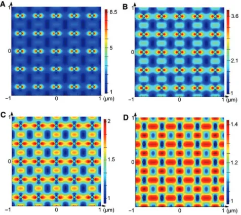
array. In Figure 10, the FDTD simulations of the square modulus of the components Ez and Ex of the electric field 30 nm above the surface are shown. We have to note that in these figures, in order to point out the field fluctua-tions, the values have been normalized by the minimum values of the electric field on the image. We observe that the localization of the electric field around the holes only
comes from Ez. Large fluctuations of the z component are observed as the maximum value, around the hole, is 200 times higher than the minimum value.
For the x component, these fluctuations are weaker, the maximum value, which is in between holes in this case, being 2.25 times higher than the minimum one. But when we look at the absolute field values, we
Figure 9: FDTD simulations of the square modulus of the electric field on the nanohole array for four distances to the surface (20, 30, 40,
70 nm). The incident wavelength is 620 nm. Values have been normalized to the minimum of each one. (A) z = 20 nm, (B) z = 30 nm, (C) z = 40 nm and (D) z = 70 nm. 1 0 –1 0 1 1 1.5 2.25 A B 1 0 0 1 1 100 200 –1 (µm) (µm)
Figure 10: Normalized square modulus of the Ex, Ez components and of the total electric field at 30 nm above the surface, simulated by FDTD.
800 T.P.L. Ung et al.: Scanning the plasmonic properties of a nanohole array
observe that the value of the Ez component is nearly 0 except around the holes. To get a better understand-ing of this behavior, we plotted in Figure 11, the ratio between the square modulus of the Ez component and the square modulus of the in plane component E‖ which corresponds to the sum of the intensity following the x direction and the intensity following the y direction, for different positions on the array. We observe that in the very near field, Ez dominates around the holes, being four times higher than E‖ 10 nm away from the surface, but quickly decreases when z increases. For all the other positions Ez is negligible.
These simulations highlight that the Ez component plays a major role in the near field and is responsible for the field localization but quickly decreases in the z direc-tion. This behavior explains the differences observed for the 2 NCs. The NC1 being more sensitive to the z compo-nent due to its dipolar orientation presents higher Purcell factors than the NC2 close to the nanoholes in the very near field. This difference vanishes when z increases. Some 60 nm away from the surface all the Purcell factors have become identical which is in good agreement with the electric field behavior. Even if the near-field FDTD simulations are not strict calculations of the LDOS, they explain the experimental results. Moreover, these simu-lations show that the fluctuations of the electric field are very fast in the x, y, and z directions. Then, to get insight into the fine LDOS, the resolution of the set-up, which is around 10 nm, could be improved. Nevertheless the obser-vations made with these NCs having different orientations allow to get information on the fine LDOS on the nanohole
array. They show specific behaviors which are in good agreement with the electric field simulations.
4 Conclusion
In summary, a deep understanding of a nanoplasmonic structure, a nanohole array, has been possible using a NC near-field nanoprobe. This probe based on a single NC attached at its end showed a good potential for probing the directional LDOS on the structure. This has been made possible thanks to the knowledge of the orientation of the NC which is determined at the very beginning of the experiment. To confirm the measurements, FDTD simula-tions have been performed. They point out the particular behavior of the near-field components of the electric field that vary like the Purcell factors measured with different nanoprobes at different positions on the array. This study shows that the influence of the z component of the elec-tric field is huge in the very near field and that the field localization around the holes comes only from it. Never-theless, as soon as we get few tens of nanometers away from the surface, the in plane components dominate. Purcell factors obtained with the nanoprobe confirm this behavior. As we are able to determine the orientaton of the NC at the end of the SNOM tip, this nanoprobe is then able to probe the near-field electromagnetic properties in the three directions of space. This makes this nanoprobe very promising for probing the fine structure of the electromag-netic environment of any nanoplasmonic structure.
Acknowledgments: This work is supported by a public
grant overseen by the French National Research Agency (ANR) as part of the “Investissements d’Avenir” pro-gram (Labex NanoSaclay, reference: ANR-10-LABX-0035, Funder Id: http://dx.doi.org/10.13039/501100001665).
References
[1] Polman A, Atwater HA. Plasmonics: optics at the nanoscale. Mater Today 2005;8:56.
[2] Walter NG, Huang CY, Manzo AJ, Sobhy MA. Do-it-yourself guide: how to use the modern single-molecule toolkit. Nat Methods 2008;5:475–89.
[3] Brolo AG. Plasmonics for future biosensors. Nat Photonics 2012;6:709–13.
[4] Jung LS, Campbell CT, Chinowsky TM, Mar MN, Yee SS. Quantita-tive interpretation of the response of surface plasmon reso-nance sensors to adsorbed films. Langmuir 1998;14:5636–48. [5] Brolo AG, Kwok SC, Moffitt MG, Gordon R, Riordon J, Kavanagh KL. Enhanced fluorescence from arrays of nanoholes in a gold film. J Am Chem Soc 2005;127:14936–41.
Figure 11: Ratio between the intensity in the z direction and the
intensity in the in plane of the array for three positions on the array shown on the MEB image.
[6] Dong J, Zhang Z, Zheng H, Sun M. Recent progress on plasmon-enhanced fluorescence. Nanophotonics 2015;4:472.
[7] Lodahl P, Mahmoodian S, Stobbe S. Interfacing single photons and single quantum dots with photonic nanostructures. Rev Modern Phys 2015;87:347–400.
[8] Bozhevolnyi SI, Mortensen NA. Plasmonics for emerging quan-tum technologies. Nanophotonics 2017;6:1185–8.
[9] Ebbesen TW, Lezec HJ, Ghaemi HF, Thio T, Wolff PA. Extraordi-nary optical transmission through sub-wavelength hole arrays. Nature 1998;391:667–9.
[10] Mrejen M, Israel A, Taha H, Palchan M, Lewis A. Near-field characterization of extraordinary optical transmission in sub-wavelength aperture arrays. Opt Express 2007;15:9129. [11] Ghaemi HF, Thio T, Grupp DE, Ebbesen TW, Lezec HJ. Surface
plasmons enhance optical transmission through subwave-length holes. Phys Rev B 1998;58:6779–82.
[12] Popov E, Nevière M, Enoch S, Reinisch R. Theory of light trans-mission through subwavelength periodic hole arrays. Phys Rev B 2000;62:16100–8.
[13] Martín-Moreno L, García-Vidal FJ, Lezec HJ, et al. Theory of extraordinary optical transmission through subwavelength hole arrays. Phys Rev Lett 2001;86:1114–7.
[14] Salomon L, Grillot F, Zayats AV, de Fornel F. Near-field distribu-tion of optical transmission of periodic subwavelength holes in a metal film. Phys Rev Lett 2001;86:1110–3.
[15] Wannemacher R. Plasmon-supported transmission of light through nanometric holes in metallic thin films. Optics Com-mun 2001;195:107–18.
[16] Treacy MMJ. Dynamical diffraction in metallic optical gratings. Appl Phys Lett 1999;75:606–8.
[17] Treacy MMJ. Dynamical diffraction explanation of the anoma-lous transmission of light through metallic gratings. Phys Rev B 2002;66:195105.
[18] Sarrazin M, Vigneron J-P, Vigoureux J-M. Role of wood anomalies in optical properties of thin metallic films with a bidimensional array of subwavelength holes. Phys Rev B 2003;67:085415.
[19] Lezec HJ, Thio T. Diffracted evanescent wave model for enhanced and suppressed optical transmission through sub-wavelength hole arrays. Opt Express 2004;12:3629. [20] Braun J, Gompf B, Weiss T, Giessen H, Dressel M, Haübner U.
Optical transmission through subwavelength hole arrays in ultrathin metal films. Phys Rev B 2011;84:155419.
[21] Spevak IS, Nikitin AY, Bezuglyi EV, Levchenko A, Kats AV. Reso-nantly suppressed transmission and anomalously enhanced light absorption in periodically modulated ultrathin metal films. Phys Rev B 2009;79:161406.
[22] Leong H, Guo J. A surface plasmon resonance spectrometer using a super-period metal nanohole array. Opt Express 2012;20:21318.
[23] Braun J, Gompf B, Kobiela G, Dressel M. How holes can obscure the view: suppressed transmission through an ultrathin metal film by a subwavelength hole array. Phys Rev Lett 2009;103:203901.
[24] Rindzevicius T, Alaverdyan Y, Sepulveda B, et al. Nano-hole plasmons in optically thin gold films. J Phys Chem C 2007;111:1207–12.
[25] Parsons J, Hendry E, Burrows CP, Auguié B, Sambles JR, Barnes WL. Localized surface-plasmon resonances in periodic nondif-fracting metallic nanoparticle and nanohole arrays. Phys Rev B 2009;79:073412.
[26] Barthes J, Bouhelier A, Dereux A, Colas des Francs G. Coupling of a dipolar emitter into one-dimensional surface plasmon. Sci Rep 2013;3:2734.
[27] Frimmer M, Chen Y, Koenderink AF. Scanning emitter lifetime imaging microscopy for spontaneous emission control. Phys Rev Lett 2011;107:123602.
[28] Schell AW, Kewes G, Hanke T, et al. Single defect centers in diamond nanocrystals as quantum probes for plasmonic nano-structures. Opt Express 2011;19:7914.
[29] Ropp C, Cummins Z, Nah S, Fourkas JT, Shapiro B, Waks E. Nanoscale imaging and spontaneous emissioncontrol with a single nano-positioned quantum dot. Nat Commun 2012;4:1447.
[30] Beams R, Smith D, Johnson TW, Oh S-H, Novotny L, Vami-vakas AN. Nanoscale fluorescence lifetime imaging of an optical antenna with a single diamond NV center. Nano Lett 2013;13:3807–11.
[31] Schell AW, Engel P, Werra JFM, Wolff C, Busch K, Benson O. Scanning single quantum emitter fluorescence lifetime imag-ing: quantitative analysis of the local density of photonic states. Nano Lett 2014;14:2623–7.
[32] Cuche A, Berthel M, Kumar U, et al. Near-field hyperspectral quantum probing of multimodal plasmonic resonators. Phys Rev B 2017;95:121402(R).
[33] Buil S, Laverdant J, Bérini B, Maso P, Hermier J-P, Qué-lin X. FDTD simulations of localization and enhance-ments on fractal plasmonics nanostructures. Opt Express 2012;20:11968.
[34] Canneson D, Mallek-Zouari I, Buil S, et al. Enhancing the fluo-rescence of individual thick shell CdSe/CdS nanocrystals by coupling to gold structures. New J Phys 2012;14:1367. [35] Ung TPL, Quélin X, Berini B, et al. Probing the hot spot
proper-ties of semicontinuous gold films through the fluorescence polarization of CdSe/CdS colloidal nanocrystals. J Nanophoton-ics 2017;11:046005.
[36] Jazi R, Ung TPL, Maso P, et al. Measuring the orientation of a single CdSe/CdS nanocrystal at the end of a near-field tip for the realization of a versatile active SNOM probe. Phys Chem Chem Phys 2018;20:16444.