HAL Id: cea-01615586
https://hal-cea.archives-ouvertes.fr/cea-01615586
Submitted on 12 Oct 2017
HAL is a multi-disciplinary open access
archive for the deposit and dissemination of
sci-entific research documents, whether they are
pub-lished or not. The documents may come from
teaching and research institutions in France or
abroad, or from public or private research centers.
L’archive ouverte pluridisciplinaire HAL, est
destinée au dépôt et à la diffusion de documents
scientifiques de niveau recherche, publiés ou non,
émanant des établissements d’enseignement et de
recherche français ou étrangers, des laboratoires
publics ou privés.
In situ cleaning/passivation of surfaces for contact
technology on III-V materials
Philippe Rodriguez, Laura Toselli, Elodie Ghegin, Fabrice Nemouchi, Névine
Rochat, Eugenie Martinez
To cite this version:
Philippe Rodriguez, Laura Toselli, Elodie Ghegin, Fabrice Nemouchi, Névine Rochat, et al.. In situ
cleaning/passivation of surfaces for contact technology on III-V materials. 2015 IEEE International
Interconnect Technology Conference and 2015 IEEE Materials for Advanced Metallization Conference
(IITC/MAM), May 2015, Grenoble, France. pp.107 - 110, �10.1109/IITC-MAM.2015.7325643�.
�cea-01615586�
In situ cleaning/passivation of surfaces for contact
technology on III-V materials
Philippe Rodriguez
∗, Laura Toselli
∗, ´
Elodie Ghegin
∗†, Fabrice Nemouchi
∗, N´evine Rochat
∗and Eug´enie Martinez
∗∗Univ. Grenoble Alpes, F-38000 Grenoble, France
CEA, LETI, MINATEC Campus, F-38054 Grenoble, France. Email: philippe.rodriguez@cea.fr
†STMicroelectronics, 850 rue Jean Monnet, BP 16, 38926 Crolles, France
Abstract—In this work we introduce the use of physical plas-mas (e.g. Ar- and He-based plasplas-mas) in order to study the in situ cleaning (prior to metal deposition) of InGaAs layers dedicated to the realisation of self-aligned contacts. For the characterisation of cleaning efficiency, we performed surface analyses like X-ray photoelectron spectroscopy and Fourier transform infrared spectroscopy in attenuated total reflection mode. The first results described in this work are encouraging. We have found efficient processes for removing totally or partially III-V native oxides.
I. INTRODUCTION- CONTEXT
The contact technology for III-V compounds has been developed since the pioneering article of Dale and Turner in 1963 [1] and the obtaining of simple Sn-based Ohmic contacts on gallium arsenide. The interest for contacting III-V materials has been growing since disruptive channel materials (including Ge and III-V materials) have been proposed for boosting the CMOS performance [2].
In recent years, for integration and scaling reasons, efforts have been made to develop non-gold Ohmic contacts and to reduce the contact dimensions from micrometric to nanometric scale. For advanced CMOS, the aim is to obtain a contact technology more cost-effective and compatible with the Si CMOS technology. In this way, we observed a transition from non-self aligned technology to a self-aligned process [3], [4]. To date, the most studied materials are the Ni-InGaAs and Co-InGaAs alloys [5], [6].
In order to propose a suitable contact technology on III-V materials, whatever the technology used (non-self aligned, self aligned, 3D. . . ), cleaning/passivation technology is highly desirable for removing particles, organic materials, metallic impurities and native oxides. The classical salicide process (eg. NiSi on Si or SiGe 30 %) involves a two-step procedure where a wet HF treatment is coupled with an in situ hot NF3/NH3 remote plasma exposure. Queue time related surface contamination caused by using only wet chemical cleaning is thus eliminated. For III-V contact technology, we strongly think that a similar strategy has to be developed. If wet chem-ical cleanings are generally proposed for realising InGaAs n-MOSFET, in situ cleanings have not been extensively studied. For deeply scaled transistors, parasitic resistances between the S/D regions and the metal contact have to be reduced as much as possible. Then, a very cleaned and native oxide free surface must be obtained before metal deposition. Thus, the absence of a dry in situ cleaning before contact metallisation could be a real issue and have strong effects on the contact microstructural and electrical characteristics.
In this work, we propose a first study using a Si CMOS technology compatible equipment in order to investigate the in situ cleaning/passivation of III-V surfaces. In this paper, we focused on results obtained with physical plasmas (e.g. Ar-and He-based plasmas).
II. EXPERIMENTAL DETAILS
All experiments described in this work were carried out in a 300 mm Applied Materials Endura® platform usually dedicated to silicide process. Apart from the metal RF PVD chambers, this tool is equipped with various pre-clean cham-bers where one can realise sample heating, hot NF3/NH3 remote plasma exposure and argon- or helium-based etching plasmas. The aim of this work is to use the pre-clean chambers usually assigned to Si-based wafers and to adapt the plasma chemistry and process parameters for the cleaning of III-V surfaces.
Because large III-V wafers are not available, we used small pieces of III-V materials on dedicated holders in order to process the samples in the 300 mm platform. In this work, we focused on results obtained for InGaAs layers grown on InP or Si substrates.
The passivation/cleaning efficiency and impact on III-V surfaces were studied by using surface analyses like X-ray pho-toelectron spectroscopy (XPS) and Fourier transform infrared (FTIR) spectroscopy in attenuated total reflection (ATR) mode. For FTIR-ATR characterisations, the data were collected using a Ge prism pressed against the sample. A Bruker IFS 55 FTIR spectrometer probed the sample via a P polarized infrared beam through the prism at an incident angle of 65 °, ensuring total reflexion on the Ge prism dioptre. XPS spectra were collected in a PHI VersaProbe II Scanning XPS Microprobe system using a monochromatic Al Kα X-ray source. In 3d,
As 3d, Ga 3d and In 4d spectra were collected with a constant pass energy of 23.5 eV leading to an overall energy resolution of 0.6 eV ; curve fitting was done by CasaXPS 2.3.16 software.
III. RESULTS
The processes based on Ar- or He-based etching plasmas are usually dedicated to the etching of tens of nanometres of silicon oxide. Thus, they have been adapted to obtain plasmas compatible with the thickness of III-V native oxides (typically ranging from 1 to 5 nanometres). One orientation was to reduce the plasma power in order to limit the impact on the III-V surface in terms of defects and roughness.
The figure 1 exhibits the normalized FTIR-ATR spectra for an InGaAs reference layer (i.e. native oxides without any treatments) and for InGaAs layers after Ar- and He-based plasma processes.
Fig. 1. Normalized Fourier transform infrared spectroscopy spectra in attenuated total reflection mode for InGaAs layers treated with Ar plasma (red line), He plasma (blue line) and without cleaning/passivation treatment (black line).
Based on literature data [7], [8], the absorption regions of III-V oxides are highlighted on figure 1. The bands observed in the 1100 – 1150 cm−1 and 1150 – 1200 cm−1regions are not attributed to III-V oxides but might be related to carbonaceous pollution from Ge prism or samples.
We clearly observe differences between the spectrum ob-tained for an uncleaned sample (black spectrum) and the spectra obtained for the plasma treated ones (red and blue spectra). Especially, the large absorption band of AsOx in the
region of 850 – 950 cm−1 is drastically reduced after surface treatment. The impact of plasma treatments on Ga and In oxides is also seen but it is less obvious.
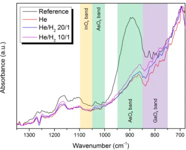
The figure 2 shows the normalized FTIR-ATR spectra for InGaAs layers treated with He (red line), He/H2 20/1 (blue line), He/H2 10/1 (magenta line) plasmas and without cleaning/passivation treatment (black line).
From the results depicted on figure 2, some tendencies can be drawn. First, the introduction of a slight percent of hydrogen in He-based plasma seems to modify the III-V oxides cleaning efficiency. The effect of hydrogen is visible for the large absorption band of AsOxin the 850 – 950 cm−1and 1000
– 1050 cm−1regions. Regarding, the shape and the intensity of the corresponding bands, AsOxremoval appears to be inversely
proportional to the H2 plasma content. It is less pronounced, but a similar tendency can be observed for GaOx bands. For In oxides, no significant effect can be detected.
Even if this technique is not often reported in literature, in this work, we demonstrated that FTIR in ATR mode is a fast and adapted technique for studying III-V material surface and discriminating efficient from non-efficient plasma processes.
For the “ATR-efficient treatments” we performed XPS
Fig. 2. Normalized Fourier transform infrared spectroscopy spectra in attenuated total reflection mode for InGaAs layers treated with He (red line), He/H2 20/1 (blue line), He/H2 10/1 (magenta line) plasmas and without cleaning/passivation treatment (black line).
analyses. An example of the obtained results is shown on fig-ure 3. The XPS results clearly evidence that plasma treatments were efficient for reducing the percentage of III-V oxides. It is obvious for As oxides where the As2O5 component is no more detected and the As2O3 is drastically reduced for
passivated samples. For In and Ga oxides, the proportion of oxide components are significantly reduced compared to the reference sample. Nevertheless, for these oxides, the oxide component after treatment is still important. We are currently working on improving the efficiency of the cleaning processes. Nonetheless, it should be noted that a queue time ranging from 30 min to 2 hours is systematically observed between sample preparation and their surface characterisation. Then a regrowth of III-V native oxides could have occurred on treated samples and slightly influence the results. We are working on an experimental protocol to limit the air exposure between sample treatment and subsequent analyses.
Depending on the plasma nature, tendencies can be ob-served thanks to XPS analyses. Both plasmas seems to be efficient for eliminating As oxides whereas Ga and In oxides are more impacted by Ar-based plasma. Further experiments are in progress to confirm these tendencies.
IV. CONCLUSION- PERSPECTIVES
We have demonstrated that a 300 mm platform usually dedicated for processing silicon wafers can be used for the in situ passivation/cleaning of III-V materials. The first results obtained with the employment of physical plasmas and de-scribed in this work are encouraging. We have found efficient processes for removing totally or partially III-V native oxides (depending on their nature). Moreover, we have observed first tendencies using different plasma varieties which will be useful in order to improve the efficiency of passivation/cleaning processes.
Impact of treatments on surface in terms of defects and roughness are under investigation (Atomic Force Microscopy
Fig. 3. XPS spectra peak fits of As 3d, In 3d and Ga 3d, In 4d regions for reference sample (top), Ar-based plasma treated sample (middle) and He-based plasma treated sample (bottom). The relative proportion of each component is indicated.
characterisations). A complete passivation/cleaning technology involving wet cleaning followed by in situ treatment is also being studied.
The processes developed in this study will be applied for the realisation of Ni-based self-aligned contacts on InGaAs and their impact in terms of electrical properties is planned to be investigated.
ACKNOWLEDGEMENTS
The authors would like to thank Thierry Baron and his team (CNRS-LTM, CEA-LETI) for the realisation of InGaAs epitaxy. This work has been partially supported by the French “Recherches Technologiques de Base” (Basis Technological Research) and RENATECH programs.
This project was supported by the public grant ANR-13-NANO-0001 MOSINAS and the Equipex FDSOI11 projects.
REFERENCES
[1] J. R. Dale and R. G. Turner, “Simple ohmic contacts on gallium arsenide,” Solid-State Electron., vol. 6, no. 4, pp. 388 – 389, 1963. [2] S. Takagi, T. Iisawa, T. Tezuka, T. Numata, S. Nakaharai, N. Hirashita,
Y. Moriyama, K. Usuda, E. Toyoda, S. Dissanayake, M. Shichijo, R. Nakane, S. Sugahara, M. Takenaka, and N. Sugiyama, “Carrier-transport-enhanced channel CMOS for improved power consumption and performance,” IEEE Trans. Electron Devices, vol. 55, no. 1, pp. 21–39, Jan 2008.
[3] Y.-C. Yeo, H.-C. Chin, X. Gong, H. Guo, and X. Zhang, “III-V MOSFETs: Surface Passivation, Source/Drain and Channel Strain Engi-neering, Self-Aligned Contact Metallization,” ECS Trans., vol. 35, no. 3, pp. 351–361, 2011.
[4] S. Takagi and M. Takenaka, “Prospective and Critical Issues of III-V/Ge CMOS on Si Platform,” ECS Trans., vol. 35, no. 3, pp. 279–298, 2011. [5] X. Zhang, H. Guo, X. Gong, Q. Zhou, Y.-R. Lin, H.-Y. Lin, C.-H. Ko, C. H. Wann, and Y.-C. Yeo, “In0.7Ga0.3As Channel n-MOSFET with
Self-Aligned Ni-InGaAs Source and Drain,” Electrochem. Solid-State Lett., vol. 14, no. 2, pp. H60–H62, 2011.
[6] Ivana, E. Y.-J. Kong, S. Subramanian, Q. Zhou, J. Pan, and Y.-C. Yeo, “CoInGaAs as a novel self-aligned metallic source/drain material for implant-less In0.53Ga0.47As n-MOSFETs,” Solid-State Electron.,
vol. 78, pp. 62–67, 2012.
[7] M. Rei Vilar, J. El Beghdadi, F. Debontridder, R. Artzi, R. Naaman, A. M. Ferraria, and A. M. Botelho do Rego, “Characterization of wet-etched GaAs (100) surfaces,” Surf. Interface Anal., vol. 37, no. 8, pp. 673–682, 2005.
[8] N. Liu and T. F. Kuech, “Interfacial chemistry of InP/GaAs bonded pairs,” J. Electron. Mater., vol. 36, no. 3, pp. 179–190, 2007.