HAL Id: tel-02003634
https://tel.archives-ouvertes.fr/tel-02003634
Submitted on 1 Feb 2019HAL is a multi-disciplinary open access archive for the deposit and dissemination of sci-entific research documents, whether they are pub-lished or not. The documents may come from teaching and research institutions in France or abroad, or from public or private research centers.
L’archive ouverte pluridisciplinaire HAL, est destinée au dépôt et à la diffusion de documents scientifiques de niveau recherche, publiés ou non, émanant des établissements d’enseignement et de recherche français ou étrangers, des laboratoires publics ou privés.
Multiresponsive and supramolecular field-effect
transistors
Tim Leydecker
To cite this version:
Tim Leydecker. Multiresponsive and supramolecular field-effect transistors. Other. Université de Strasbourg, 2015. English. �NNT : 2015STRAF056�. �tel-02003634�
1
UNIVERSITÉ DE STRASBOURG
ÉCOLE DOCTORALE DES SCIENCES CHIMIQUES
UMRS 7006 – Institut de science et d’ingénierie Supramoléculaires
THÈSE
présentée par :
Tim LEYDECKER
soutenue le : 11 Décembre 2015
pour obtenir le grade de :
Docteur de l’université de Strasbourg
Discipline/ Spécialité
: Chimie
Multiresponsive and supramolecular
field-effect transistors
THÈSE dirigée par :
M.
SAMORÌ
Paolo
Professeur, Université de Strasbourg, FranceRAPPORTEURS :
M. LAZZARONI Roberto
Professeur, Université de Mons, BelgiqueM. MARLETTA Giovanni
Professeur, Université de Catania, ItalieAutres membres du jury :
M. HEISER Thomas
Professeur, Université de Strasbourg, France Examinateur internei
R
ESUME DE LA THESE
Le sujet de cette thèse est l'optimisation performances des transistors à effet de champ organiques (OFET) et l'intégration de fonctionnalités supplémentaires dans des OFET par mélange des composants moléculaires, chacun conférant une caractéristique bien distincte.
Les semi-conducteurs organiques ont fait l'objet d'une activité de recherche approfondie au cours des dernières décennies, car ils représentent des composants clés pour les applications technologiques dans l'opto-électronique tels que l'électronique de grande échelle, les écrans et les senseurs1-7. Ils présentent de nombreux avantages par rapport à leurs homologues inorganiques (ajustement de leurs propriétés physiques par le biais fonctionnalisation chimique, traitement à faible coût en utilisant des conditions douces, intégration sur des supports flexibles, etc.)8. Toutefois, pour une mise sur le marché, la plupart des semi-conducteurs organiques déposés en solution doivent encore atteindre des mobilités à effet de champ comparables à ceux du silicium amorphe. Ces mobilités faibles résultent de la faible cristallinité des couches semi-conductrices en raison d'une taille de grain typique qui est normalement beaucoup plus faible que la longueur de canal du dispositif.9 En outre, les propriétés des dispositifs organiques sont fortement dépendants de leur interface étant donné l'importance que les interfaces métal / semi-conducteur et diélectrique / semi-conducteur jouent dans la détermination de la mobilité du transistor à effet de champ ainsi que la tension de seuil.10-11 Par conséquent, une ingénierie de l’interface optimale est nécessaire, car elle affectera la mobilité et la tension seuil.
Les petites molécules semi-conductrices ont démontré des performances électriques intéressantes, en partie en raison de leur tendance prononcée à former des domaines cristallins par rapport à leurs homologues polymères.12-18 En particulier, les dispositifs d’oligothiophènes hexaméthyl-substitués, tels que le di-hexylquaterthiophene (DH4T) sont des systèmes modèles facilement accessibles qui ont fait leurs preuves pour afficher une grande résistance à l'environnement, en raison de leur assemblage dense et de chaînes hexyles agissant comme une couche de passivation en plus de leur performance de transport de charges dans les transistors. Pour des films sublimés le plus forte mobilité observée (μ) est de 0,09 cm² / Vs. En ce qui concerne les films déposés par solution, les valeurs les plus élevées de mobilité
ii
trouvées dans la littérature sont de μ = 0,043 cm² / Vs pour les dispositifs imprimés par jet d'encre et de μ = 0,012 cm² / Vs pour les films déposés par enduction centrifuge, révélant une grande marge pour l’amélioration d’un point de vue de la fabrication des dispositifs.19-21 La morphologie et la cristallographie de films DH4T ont été plus récemment étudiées par Thierry et al., montrant comment DH4T peut s’auto-assembler en une structure cristalline hautement ordonnée. Dans leur étude, l'ordre cristallin dans les domaines produits par sublimation sous vide était similaire à celui trouvé dans des domaines cristallins issus d’une solution. Les dispositifs par solution de haute mobilité peuvent être produits donc si le processus cinétique régi par la croissance du film est contrôlée pour obtenir de grands domaines cristallins, éliminant ou réduisant l'effet de joints de grains, qui sont préjudiciables pour le transport de charge.22-24
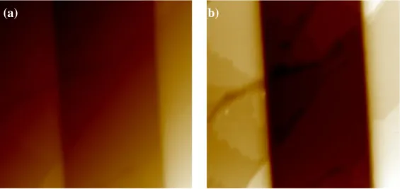
Initialement, cette molécule prototype a été testée dans trois solvants chlorés différents à savoir le chloroforme (CHCl3), le 1,2-dichlorobenzène (DCB) et le chlorobenzène (CB). Le choix du solvant a été jugée crucial pour les performances du dispositif. En particulier, la caractérisation morphologique multi-échelle, de centaines d’µm jusqu’à l'échelle nanométrique, a été réalisée à la fois par microscopie optique (OM) et à force atomique (AFM). Les morphologies des films préparés par déposition de goutte de solution de 1 mg / ml de DH4T dans du chloroforme, du chlorobenzène (CB) et du dichlorobenzène (DCB) ont été comparées. La surface des films de DH4T déposés à partir de solution dans le chloroforme est constituée de petits cristaux rarement reliés entre eux, tandis que les films obtenus en utilisant le chlorobenzène ou le dichlorobenzène comme solvant affichent des domaines cristallins plus grands et plus uniformes sur les images OM. Tous les films englobés dans cette étude présentent un haut degré de cristallinité tel que confirmé par analyse par diffraction à incidence rasante des rayons X. L'uniformité de film sans présence de défauts sur une plus grande échelle pour les films de chloro- et dichlorobenzène diminue significativement la présence des joints de grains. Inversement, les films déposés à partir CHCl3 présentent une très forte rugosité de surface à échelle méso, tandis que les films préparés à partir de CB ont montré une diminution de la rugosité. Les films préparés à partir de solutions DCB exposées une rugosité encore plus faible.
La procédure qui présentait la meilleure mobilité, à savoir 70 µL de DH4T à 5 mg / ml dans le DCB et une vitesse d'évaporation de 0,1, sera désigné comme la «procédure optimisée ». Elle a été reproduite avec succès sur plus de 110 dispositifs avec l'hexaméthyldisilazane (HMDS) en tant que traitement de surface. Il convient de noter, en
iii
dépit du fait que la déposition par goutte est une technique de dépôt qui est censé conduire à des performances inégales de dispositif à dispositif en raison de la variation d'épaisseur dans le plan xy, la présence de grands cristaux plats couvrant des centaines de micromètres a permis la fabrication de dispositifs dont les caratéristiques électriques dont la mobilités avec des écarts types qui sont absolument comparables à ceux obtenus pour des films produits par enduction centrifuge. De manière significative, contrairement aux dispositifs HMDS fonctionnalisés préparés par la procédure optimisée, les courbes de sortie n’indiquent pas la présence d'une résistance de contact élevée lorsque l'octadécyltrichlorosilane (OTS) est utilisé pour fonctionnaliser la surface du diélectrique d'oxyde de silicium. Les dispositifs ont démontré des mobilités allant jusqu'à 0,10 cm² / Vs et des rapports Ion / Ioff jusqu'à 5 × 10⁷. Lorsque la procédure optimisée est utilisé, les cristallites comblent facilement l’espace entre les électrodes source et drain. En outre, la morphologie des cristallites, suivant le profil des électrodes, semble indiquer l'absence de sites de nucléation dans la région inter-électrodique. Cela indique que la formation de cristallites ne commence pas dans le solvant mais seulement plus tard, ces structures "atterrissant" sur les électrodes et s’étendant par auto-assemblage.
Afin de démontrer cette hypothèse, DH4T a été mélangé avec une molécule similaire, DH2T (dihexylbithiophene). 7 échantillons ont été produits, avec des quantités croissantes de DH2T dans le mélange, et les performances électriques ont été mesurées. Les trois scénarios d'assemblage extrêmes sont les suivants: (a) un film entièrement mélangé avec présence d'impuretés DH2T l'intérieur des grains de DH4T, conduisant à une diminution probable de cristallinité; (b) une séparation de phase horizontale avec les îlots de DH2T entourés par du DH4T et (c) la ségrégation verticale de phase avec une couche de molécule la plus légère et la plus soluble (DH2T) sur le dessus. De manière surprenante, les données obtenues par TOF-SIMS indiquent que la couche de DH2T est présente à l'interface entre le diélectrique et la couche semi-conductrice (l'interface étant de 50:50 DH4T: DH2T sur un mélange 99: 1). Ce résultat tend à confirmer l'idée que la nucléation de cristallites DH4T ne se produit pas dans la région du canal, mais plutôt dans la partie supérieure de la goutte de solution déposée sur les électrodes. Les performances électriques ont été testées pour les films résultants des solutions mixtes. Une forte baisse de performances électriques a été constatée lors de l'addition de très petites quantités de DH2T au mélange (0.1%). DH2T étant une petite molécule isolante, la baisse des performances électriques prouve la présence de DH2T à l'interface avec le diélectrique. Cela montre que le test électrique peut être utilisé comme un outil non destructif de caractérisation de l'interface.
iv
Nous avons employé les connaissances acquises sur les (macro)molécules et l’auto-assemblage multi-composant afin d'intégrer une nouvelle fonctionnalité dans un dispositif semi-conducteur par voie de mélange. Parmi les différentes classes de molécules, les systèmes photochromiques ont montré des résultats prometteurs en tant que commutateurs moléculaires, mais très peu de caractéristiques des (semi)conductivité ainsi qu’une fatigue non négligeable. La commutation optique entre deux états adressables indépendamment conduit à des changements à la fois au niveau moléculaire et l'échelle macroscopique. Au niveau moléculaire, nous observons des changements structurels et électroniques, des changements réversibles de la géométrie, des moments dipolaires, de la conjugaison π, de réversibles, de la bande interdite, etc.25 La modification des propriétés macroscopiques lors de la commutation comprennent des changements dans la forme, le comportement de l'agrégation et de la conductance. La molécule que nous avons choisi est un diaryléthène (DAE-Me), synthétisé dans le cadre d'une collaboration à long terme, par le groupe du professeur Stefan Hecht à l'Université Humboldt de Berlin. Étant donné que ces diaryléthènes alkyle-substitués ne présentent pas de comportement semi-conducteur, ils ont été mélangés avec un polymère semi-conducteur bien connu, à savoir P3HT. La HOMO de P3HT se trouve entre celles du DAE-Me ouvert et la forme fermée. En raison de ce fait, lorsque le diaryléthène est dans la forme ouverte, son HOMO agit comme un centre de diffusion.26-27 Néanmoins, lorsque le diaryléthène est dans la forme fermée, les charges se retrouvent piégés réduisant ainsi le courant | IDS | obtenu. Etant donné que le diaryléthène est thermodynamiquement stable dans les deux formes, cet effet a été utilisé afin de stocker des informations et de créer des mémoires à plusieurs niveaux.
Un montage de laser avec des temps d'éclairage de 3 ns à haute intensité a été utilisé afin d'enquêter sur la commutation photo-induite sur les moments pertinents dans l'électronique moderne par irradiation. Une impulsion laser de 3-ns (λ = 313 nm) à intensité modulable a irradié l'échantillon toutes les dix secondes conduisant à une diminution progressive du courant contrôlée par le nombre d'impulsions. Chaque impulsion générant un palier de diminution de courant ΔIDS en raison de l'augmentation du nombre de molécules de diaryléthène dans la forme ouverte, qui ont basculé vers leur forme fermée. Nous avons réussi à construire un dispositif de 400 niveaux d'intensité de courant, pour atteindre une capacité de stockage de données sur huit bits (256 niveaux). Par réduction de l'intensité lumineuse en utilisant des filtres, nous avons montré que la hauteur des marches est fonction de la densité de puissance surfacique parce que le nombre de molécules subissant une isomérisation est directement lié à la densité des photons frappant la zone active du dispositif. Par conséquent, afin d'augmenter le nombre de paliers, l'intensité lumineuse peut être modulée d’une intensité
v
faible à élevée. Le nombre de paliers serait seulement limité par le bruit dans le signal (conduisant à 5000 étapes pour l'expérience présentée) pour un nombre maximal théorique d'étapes égal au nombre de diaryléthènes dans le mélange.
Dans l'intérêt de démontrer la possible mise en œuvre des mémoires dans les applications électroniques novatrices, toute la procédure a été transférée sur un substrat flexible, la abandonnant sur les couches rigides inorganiques à base de silicium pour des couches polymères de polyéthylène téréphtalate (PET), le poly (méthacrylate de méthyle)) (PMMA) et le poly (4-vinylphénol) (PVP). Les dispositifs ont été caractérisés électriquement et les mobilités sont comparables à celles sur oxyde de silicium (supérieures à 10-3 cm² / Vs). Les capacités de commutation ont été testées sur plusieurs cycles de commutation dynamiques. Nous avons constaté que les dispositifs pouvaient être basculés de la forme fermée à ouverte et vice-versa. Des courbes dynamiques IDS-temps avec de petites étapes d'illumination à 313 nm indiquent la capacité de l'appareil à fonctionner comme une mémoire multi-niveaux de 4 bits (16 niveaux distincts). En outre, la caractérisation électrique a été réalisée sur le dispositif après les étapes successives de flexion (rayons de courbure de 29 mm, 17,5 mm, 10 mm, 8 mm et 6 mm). Après flexion, les performances étaient encore comparables à celles observées avant flexion à chaque rayon de courbure pendant 60 secondes, avec des pertes mineures en termes de courant et un léger changement dans la tension de seuil, prouvant qu’avec de l'optimisation, la mémoire organique 3-terminaux étudiée peut être utilisée dans l'électronique flexible.
Visant une enquête plus approfondie sur l’implémentation de fonctions par le biais de mélanges, deux polymères, IIDDT-C3 et N2200, ont été sélectionnés pour leurs fortes capacités de transport de charge respectivement de type p et de type n, ainsi qu’une légère ambipolarité. Les deux polymères contenant des squelettes de thiophène et des chaînes alkyle similaires à nos molécules modèles DH4T et P3HT, elles démontraient ainsi un bon potentiel de mélange. L'objectif de cette étude en cours est la fabrication de dispositifs ambipolaires. Des dispositifs avec des quantités différentes de IIDDT-C3 dans le mélange ont été produits, avec de bonnes performances électriques. Un dispositif ambipolaire parfaitement équilibré a été produit à un mélange 50/50 de IIDDT-C3 et N2200. Cette approche est très intéressante car elle permet l’ambipolarité à la demande et pourrait être adaptée à d'autres polymères à mobilités plus élevés.
vi
En résumé, notre étude comparative sur la structure par rapport à la fonction dans des OFETs basés sur DH4T en solution a révélé que par l’optimisation des conditions de formation d'un film par un choix judicieux de la méthode de traitement, de type de solvant, de la fonctionnalisation des interfaces et en particulier en réglant la vitesse d'évaporation du solvant il est possible de conduire l'auto-assemblage moléculaire vers la formation d'architectures hautement ordonnées présentant des caractéristiques électriques améliorées. De manière significative, leur utilisation comme composants électro-actifs dans des OFETs conduit à des performances de électriques qui sont au-delà de l'état de l’art pour les transistors basés sur DH4T, même lorsque comparé à ceux produits par sublimation faits avec la même molécule. En particulier, les mobilités de type p atteignant 0,10 cm² / Vs et des ratios Ion / Ioff supérieurs à 107 ont été atteints. Nos résultats confirment sans ambiguïté que l'adaptation des interfaces est la clé de bonnes performances électriques. Notre méthode de traitement pour fabriquer des dispositifs à haute mobilité est compatible avec les applications de grande échelle offrant ainsi une voie vers l'électronique organique qui satisfait l'équilibre nécessaire entre la performance et la facilité de fabrication. Combiner le matériau avec DH2T a donné des informations supplémentaires sur le processus de cristallisation de DH4T qui se déroule au-dessus des électrodes. Ces résultats ont été confirmés par TOF-SIMS ainsi que la caractérisation électrique des films produits à partir de mélanges DHnT.
En mélangeant un polymère semi-conducteur avec une petite molécule photochromique, nous avons montré qu'il était possible de construire des dispositifs de mémoire à 3 terminaux ayant des caractéristiques remarquables. Surtout, la possibilité de définir plusieurs niveaux de courant distincts ouvre la voie à des mémoires à haute densité, avec des unités de mémoire 8-bits (256+ niveaux). Le temps d'éclairage utilisé pour le montage laser était à l’échelle de la nanoseconde, une échelle de temps qui est nécessaire pour l'électronique de la vie réelle. Il a été montré que cette approche pourrait être appliquée aussi sur des substrats flexibles. En outre, les très bonnes capacités de conservation des données des dispositifs et la fiabilité après plusieurs cycles d'écriture-effacement rend cette approche idéale pour l'électronique de l’avenir. Etant donné que cette approche est très polyvalente et non limité à une paire précise de molécules, en vue d’une alternative à l'encapsulation, le P3HT sensible à l'air pourrait être remplacé par un semi-conducteur de type p différent avec des niveaux d'énergie similaires, menant à des courants potentiellement plus élevés (d'où un nombre accru de niveaux possibles). En outre, les électrodes peuvent être imprimées à faible coût, sur de grandes surfaces pour une production de masse facilitée. En mélangeant deux polymères, il fut possible d'obtenir l’ambipolarité à la demande avec un rapport de mobilités
vii
« type p / type n » allant de 10-2 et 103. Cette approche pourrait être adaptée à d'autres paires de semi-conducteurs et fait partie d'une étude en cours avec d'autres polymères.
Toutes ces études ont démontré que conférer à un matériau des fonctionnalités supplémentaires par mélange est une approche très efficace, réduisant les coûts et les difficultés de traitement par rapport aux techniques reposant sur l’utilisation de couches distinctes de matériaux. La sélection minutieuse des conditions de traitement (solvant, concentration, rapport de mélange, traitement de la surface, etc.) conduisent à de bonnes performances électriques pour chaque matériau et mélange étudié.
viii
A
BSTRACT
The topic of this thesis is the optimization of organic field-effect transistor (OFET) performances and the integration in OFET of additional functionalities through blending molecular components each one imparting a well-distinct characteristic to the material.
Organic semiconductors have been the focus of an extensive research activity during the past decades because they represent key active components for technological applications in opto-electronics such as large-area electronics, displays and sensing. They hold numerous advantages when compared to their inorganic counterparts (tunability of their physical properties via chemical functionalization, their low cost processing using mild conditions integration onto flexible supports, etc.). However, in order to enter the marketplace, most of the solution-processable organic semiconductors still need to reach field-effect mobilities comparable to those of amorphous silicon. These low device mobilities arise from the poor crystallinity of the semiconducting layers due to a typical grain size which is normally much smaller than the channel length of the device. Furthermore, organic devices' properties are strongly interface-dependent given the importance that metal/semiconductor and dielectric/semiconductor play in determining the field-effect transistor’s mobility as well as threshold voltage. Hence, optimal interface engineering is required because it will ultimately affect mobility and threshold voltage.
Small semiconducting molecules have proven to exhibit interesting electrical performances, partly due to their pronounced tendency to form crystalline domains when compared to their polymeric counterparts. In particular, hexamethyl-substituted oligothiophene based devices, such as di-hexylquaterthiophene (DH4T) are easily accessible model systems that have proven to display a high resistance to the environment, due to their dense packing and hexyl chains working as a passivation layer in addition to their charge transport performance in transistors. For vacuum deposited films the highest observed mobility (µ) amounted to 0.09 cm²/Vs. As far as solution-processed films are concerned, the highest reported mobility values amounted to µ=0.043 cm²/Vs for ink-jet printed devices and of µ=0.012 cm²/Vs for spin-coated films, indicating that there is much room for improvement
ix
on the processing side. Morphology and crystallographic parameters of DH4T films have been more recently investigated by Thierry et al. showing how DH4T can self-assemble into a highly ordered crystalline structure. In their study, the crystalline order within domains produced by vacuum sublimation was similar to that found in crystalline domains grown from solution. High mobility solution-processed devices can be therefore produced if the kinetically governed process of film growth is controlled to achieve large crystalline domains, eliminating or reducing the effect of grain boundaries, which are detrimental for the charge transport.
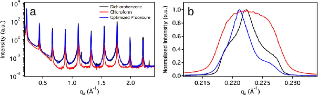
Initially this prototypical molecule was tested in three different chlorinated solvents namely chloroform (CHCl3), 1,2-dichlorobenzene (DCB) and chlorobenzene (CB). The choice of the solvent was found to be crucial for the device performance. In particular, multiscale morphological characterization, from the hundreds-of-μm down to sub-μm scale, was carried out both by optical (OM) and atomic force (AFM) microscopy. The morphologies of DH4T films prepared by drop-casting from 1 mg/mL DH4T solution in chloroform, chlorobenzene (CB) and dichlorobenzene (DCB) were compared. The surface of the DH4T films deposited from chloroform solution consists of small crystals often not interconnected, whereas the films obtained using chlorobenzene or dichlorobenzene as a solvent display larger and more uniform crystalline domains in OM images. All films encompassed in this study exhibit high degree of crystallinity as confirmed by grazing incidence X-ray diffraction analysis. The film uniformity without presence of defects over a larger scale for chloro- and dichlorobenzene films does significantly decrease the occurrence of grain boundaries. Conversely, films deposited from CHCl3 displayed very high surface roughness on the mesoscale, while films prepared from CB showed a decreased roughness. Films prepared from DCB solutions exhibited an even smaller roughness.
The procedure that exhibited the best mobility, i.e. 70 µL of DH4T at 5 mg/mL drop-cast from DCB, evaporation rate of 0.1, will be referred to as the “optimized procedure”. It has been successfully reproduced on over 110 devices using hexamethyldisilazane (HMDS) as a surface treatment. Noteworthy, in spite of the fact that drop-casting is a deposition technique which is supposed to lead to uneven device-to-device performances due to thickness variation in the x-y plane, the presence of large flat crystals spanning over hundreds of micrometers allowed for the fabrication of devices whose electrical parameters featured mobilities with standard deviations which were absolutely comparable to those achieved in spin-coated films. Significantly, in contrast to HMDS-functionalized devices prepared with the optimized procedure, output curves do not indicate the presence of a high contact resistance when
x
octadecyltrichlorosilane (OTS) is used to functionalize the surface of the dielectric silicon oxide. The devices exhibit mobilities up to 0.10 cm²/Vs and Ion/Ioff up to 5×10⁷.
When the optimized procedure is used, the crystallites readily bridge the source and drain electrodes. Furthermore, the morphology of the crystallites, bridging and following the profile of the electrodes, seems to suggest the absence of nucleation sites in the interelectrodic region. This indicates that the formation of the crystallites does commence in the solvent and only later these structures “land” on the electrodes and expand via self-assembly.
In order to demonstrate this hypothesis, DH4T was blended with a similar molecule, DH2T (dihexylbithiophene). 7 samples were produced, with increasing amounts of DH2T in the blend, and the electrical performances were measured. The three extreme assembly scenarios are: (a) a fully blended film with presence of the DH2T impurities within the DH4T grains, leading to a likely decrease of crystallinity; (b) a horizontal phase segregation with islands of DH2T surrounded by DH4T and (c) vertical phase segregation with a layer of the lightest and most soluble molecule (DH2T) on top. Surprisingly, data from TOF-SIMS measurements indicate that the DH2T layer is present at the interface between dielectric and within the semiconducting layer (the interface being 50:50 DH4T:DH2T on a 99:1 blend). This result tends to corroborate the idea that the nucleation of DH4T crystallites does not happen within the interchannel region, but rather at the top of the solution drop deposited on the electrodes. The electrical performances were tested for the films resulting of blended solutions. A strong decrease of electrical performances was found upon addition of very small quantities of DH2T to the blend. Since DH2T is a insulating small molecule, the drop in electrical performances proves the presence of the DH2T at the interface with the dielectric. This shows that electrical testing can be used as a non-destructive tool of characterization of the interface.
We profited of the knowledge acquired on (macro)molecules and multicomponent self-assembly in order to to incorporate a novel functionality into a semiconducting device via blending. Among various classes of molecules, photochromic systems have shown promising results as molecular switches, but very little (semi)conducting characteristics and not negligible fatigue. Optical switching between two independently addressable states leads to changes both at the molecular and the macroscopic scale. At the molecular level, we observe reversible structural and electronic changes in the geometry, dipole moments, π-conjugation,
xi
bandgap, etc. Modifications of macroscopic properties upon switching include changes in shape, aggregation behavior and conductance. The molecule we have chosen is diarylethene (DAE-Me), synthesized, in the frame of a long-term collaboration, by the group of Prof. Stefan Hecht at Humboldt University Berlin. Given that these alkyl substituted diarylethenes did not display any semiconducting behavior, they have been blendend with a well-known semiconducting polymer, i.e. P3HT. The HOMO level of P3HT sits in-between that of DAE-Me in the open and the closed form. Because of this reason when the diarylethene is in the open form, its HOMO acts as a scattering center. On the other hand, when the diarylethene is in the closed form, charges get trapped reducing thereby resulting the |IDS| current. Since the diarylethene is thermodynamically stable in both forms, this effect was used in order to store information and build multilevel memories.
A laser-setup with illumination times of 3 ns at high intensity was used in order to investigate the photo-induced switching upon irradiating times relevant in modern electronics. A 3-ns laser pulse (λ = 313 nm) at modulable intensity was shone on the sample every ten seconds leading to a progressive current decrease controlled by the number of pulses. Each pulse generated a ΔIDS step decrease owing to the increasing number of diarylethene molecules in the open form which are turned into their closed form. We have successfully built a 400 current-intensity levels device, reaching a data storage capacity over 8 bit (256 levels). By reduction of the light intensity using filters, we have shown that the step height is dependent on the areal power density because the number of molecules undergoing isomerization is directly linked to the density of the photons hitting the active area of the device. Therefore, in order to increase the number of steps, the light intensity could be modulated from low to high. The number of steps would only be limited by the noise in the signal (leading to 5000 steps in the presented experiment) for a theoretical maximum number of steps equal to the number of diarylethenes in the blend.
In the interest of demonstrating possible implementation of the memory-devices into novel electronic applications, the whole procedure was transferred onto a flexible substrate, trading the rigid inorganic silicon based layers for polymeric sheets of polyethylene terephtalate (PET), Poly(methyl methacrylate)) (PMMA) and poly(4-vinylphenol) (PVP). The devices were electrically characterized and the measured field-effect mobilities were comparable to those on silicon oxide (exceeding 10-3 cm²/Vs). Switching capabilities were tested over multiple dynamic switching cycles. We have found that the devices could be switched closed and back open. Dynamic IDS-time curves with small illumination steps at 313
xii
nm indicate the ability of the device to work as a 4-bit multilevel memory (16 distinct levels). Furthermore, electrical characterization was performed on the device after successive bending steps (bending radii of 29 mm, 17.5 mm, 10 mm, 8 mm and 6 mm). Post-bending performances were still comparable to those observed before bending at each bending radius for 60 seconds, with only minor losses in terms of current and a slight shift in the threshold voltage, proving that with further optimization, the studied organic 3-terminal memory devices could be introduced into flexible electronics.
Aiming further investigation of function implementation through blending, two polymers, IIDDT-C3 and N2200, were selected for their strong capabilities of respectively p-type and n-p-type charge transport, as well as slight ambipolarity. Both polymers contain thiophene backbones and alkyl chains similarly to our model molecules DH4T and P3HT, therefore demonstrating good blending potential. The objective of this ongoing study is the fabrication of ambipolar devices. Devices with different quantities of IIDDT-C3 in the blend were produced, with good electrical performances. A perfectly balanced ambipolar device was produced at a 50/50 blend of IIDDT-C3 and N2200. This approach is very interesting as it allows ambipolarity on demand and could be adapted to other polymers with higher mobilities.
In summary, our comparative study on the structure vs. function relationship in solution processed DH4T based OFETs revealed that by optimizing the conditions of film formation via judicious choice of processing method, solvent type, interfaces functionalization and in particular by tuning the rate of solvent evaporation it is possible to drive the molecular self-assembly towards the formation of highly ordered low-dimensional architectures exhibiting enhanced electrical characteristics. Significantly, their use as electroactive components in OFETs led to device performances that are beyond the state-of-the-art for DH4T-base transistors, even when compared to vacuum processed OFETs made with the same molecule. In particular, p-type mobilities as high as 0.10 cm²/Vs and Ion/Ioff currents exceeding 107 were achieved. Our results unambiguously confirm that the tailoring of interfaces is key. Our processing method to achieve high mobility devices is compatible with large-area applications thus providing a pathway towards organic electronics that satisfies the needed balance between performance and processability. Blending the material with DH2T gave additional insight into the crystallization process of DH4T that takes place above the
xiii
electrodes. Those results were confirmed by TOF-SIMS as well as electrical characterization of the films produced from DHnT blends.
By blending a semiconducting polymer with a photochromic small molecule, we have shown that it is possible to build 3-terminal memory-devices with impressive characteristics. Above all, the ability to define many distinct current-levels paves the way for high-density memories, with 8-bit memory units (256+ levels). Illumination times using the laser-setup were in the ns rage, a timescale that is necessary for real-life electronics. It has been shown that this approach could be implemented also onto flexible substrates. Furthermore, the very good data-retention capabilities of the devices and the reliability after many write-erase cycles makes this approach ideal for the electronics of the future. Since this approach is very versatile, as an alternative to encapsulation, the air-sensible P3HT could be replaced by an alternative p-type semiconductor with similar energy levels, leading to potentially higher currents (hence an increased possible number of steps). Additionally, the electrodes could be printed for facilitated low-cost, large-area mass production. By blending two polymers it was possible to achieve ambipolarity on demand with any kind of p/n ratio ranging from 10-2 to 103. This approach could be adapted to other p-type/n-type pairs and is part of an ongoing study with other polymers.
All these studies have demonstrated conferring to a material additional functionalities via blending is a very efficient approach, reducing costs and processing difficulties as compared to techniques relying on the processing of separate layers of materials. The careful selection of processing conditions (solvent, concentration, blend ratio, surface treatment, etc.) lead to good electrical performances of each material and blend.
xiv
R
EFERENCES
1. Sirringhaus, H.; Brown, P. J.; Friend, R. H.; Nielsen, M. M.; Bechgaard, K.; Langeveld-Voss, B. M. W.; Spiering, A. J. H.; Janssen, R. A. J.; Meijer, E. W.; Herwig, P.; de Leeuw, D. M., Two-Dimensional Charge Transport in Self-Organized, High-Mobility Conjugated Polymers. Nature 1999, 401 (6754), 685-688.
2. Orgiu, E.; Samorì, P., 25th Anniversary Article: Organic Electronics Marries Photochromism: Generation of Multifunctional Interfaces, Materials, and Devices. Adv. Mater. 2014, 26 (12), 1827-1845.
3. Tobjörk, D.; Österbacka, R., Paper Electronics. Adv. Mater. 2011, 23 (17), 1935-1961.
4. Xu, Y. Y.; Zhang, F.; Feng, X. L., Patterning of Conjugated Polymers for Organic Optoelectronic Devices. Small 2011, 7 (10), 1338-1360.
5. Dimitrakopoulos, C. D.; Malenfant, P. R. L., Organic Thin Film Transistors for Large Area Electronics. Adv. Mater. 2002, 14 (2), 99-117.
6. Nomoto, K.; Hirai, N.; Yoneya, N.; Kawashima, N.; Noda, M.; Wada, M.; Kasahara, J., A High-Performance Short-Channel Bottom-Contact OTFT and Its Application to AM-TN-LCD. IEEE Trans. Electron Devices 2005, 52 (7), 1519-1526.
7. Torsi, L.; Farinola, G. M.; Marinelli, F.; Tanese, M. C.; Omar, O. H.; Valli, L.; Babudri, F.; Palmisano, F.; Zambonin, P. G.; Naso, F., A Sensitivity-Enhanced Field-Effect Chiral Sensor. Nat. Mater. 2008, 7 (5), 412-417.
8. Arias, A. C.; MacKenzie, J. D.; McCulloch, I.; Rivnay, J.; Salleo, A., Materials and Applications for Large Area Electronics: Solution-Based Approaches. Chem. Rev. 2010, 110 (1), 3-24.
9. Shtein, M.; Mapel, J.; Benziger, J. B.; Forrest, S. R., Effects of Film Morphology and Gate Dielectric Surface Preparation on the Electrical Characteristics of Organic-Vapor-Phase-Deposited Pentacene Thin-Film Transistors. Appl. Phys. Lett. 2002, 81 (2), 268-270.
10. Cornil, J.; Beljonne, D.; Calbert, J. P.; Brédas, J. L., Interchain Interactions in Organic Pi-Conjugated Materials: Impact on Electronic Structure, Optical Response, and Charge Transport. Adv. Mater. 2001, 13 (14), 1053-1067.
11. Liscio, A.; Orgiu, E.; Mativetsky, J. M.; Palermo, V.; Samorì, P., Bottom-up Fabricated Asymmetric Electrodes for Organic Electronics. Adv. Mater. 2010, 22 (44), 5018-5023.
12. Halik, M.; Klauk, H.; Zschieschang, U.; Schmid, G.; Ponomarenko, S.; Kirchmeyer, S.; Weber, W., Relationship between Molecular Structure and Electrical Performance of Oligothiophene Organic Thin Film Transistors. Adv. Mater. 2003, 15 (11), 917-922.
13. Payne, M. M.; Parkin, S. R.; Anthony, J. E.; Kuo, C. C.; Jackson, T. N., Organic Field-Effect Transistors from Solution-Deposited Functionalized Acenes with Mobilities as High as 1 Cm(2)/V-S. J. Am. Chem. Soc. 2005, 127 (14), 4986-4987.
14. Sergeyev, S.; Pisula, W.; Geerts, Y. H., Discotic Liquid Crystals: A New Generation of Organic Semiconductors. Chem. Soc. Rev. 2007, 36 (12), 1902-1929.
15. Leufgen, M.; Rost, O.; Gould, C.; Schmidt, G.; Geurts, J.; Molenkamp, L. W.; Oxtoby, N. S.; Mas-Torrent, M.; Crivillers, N.; Veciana, J.; Rovira, C., High-Mobility Tetrathiafulvalene Organic Field-Effect Transistors from Solution Processing. Org. Electron. 2008, 9 (6), 1101-1106.
16. Mas-Torrent, M.; Masirek, S.; Hadley, P.; Crivillers, N.; Oxtoby, N. S.; Reuter, P.; Veciana, J.; Rovira, C.; Tracz, A., Organic Field-Effect Transistors (OFETs) of Highly Oriented Films of Dithiophene-Tetrathiafulvalene Prepared by Zone Casting. Org. Electron. 2008, 9 (1), 143-148.
17. Gao, P.; Beckmann, D.; Tsao, H. N.; Feng, X.; Enkelmann, V.; Baumgarten, M.; Pisula, W.; Müllen, K., Dithieno 2,3-D;2 ',3 '-D ' Benzo 1,2-B;4,5-B ' Dithiophene (DTBTD) as Semiconductor for High-Performance, Solution-Processed Organic Field-Effect Transistors. Adv. Mater. 2009, 21 (2), 213-216. 18. Cavallini, M.; D'Angelo, P.; Criado, V. V.; Gentili, D.; Shehu, A.; Leonardi, F.; Milita, S.; Liscio, F.;
Biscarini, F., Ambipolar Multi-Stripe Organic Field-Effect Transistors. Adv. Mater. 2011, 23 (43), 5091-5097.
19. Generali, G.; Dinelli, F.; Capelli, R.; Toffanin, S.; di Maria, F.; Gazzano, M.; Barbarella, G.; Muccini, M., Correlation among Morphology, Crystallinity, and Charge Mobility in Ofets Made of Quaterthiophene Alkyl Derivatives on a Transparent Substrate Platform. J. Phys. Chem. C 2011, 115 (46), 23164-23169.
xv
20. Song, D. H.; Choi, M. H.; Kim, J. Y.; Jang, J.; Kirchmeyer, S., Process Optimization of Organic Thin-Film Transistor by Ink-Jet Printing of DH4T on Plastic. Appl. Phys. Lett. 2007, 90 (5), 053504.
21. Garnier, F.; Hajlaoui, R.; El Kassmi, A.; Horowitz, G.; Laigre, L.; Porzio, W.; Armanini, M.; Provasoli, F., Dihexylquaterthiophene, a Two-Dimensional Liquid Crystal-Like Organic Semiconductor with High Transport Properties. Chem. Mater. 1998, 10 (11), 3334-3339.
22. Granstrom, E. L.; Frisbie, C. D., Field Effect Conductance Measurements on Thin Crystals of Sexithiophene. J. Phys. Chem. B 1999, 103 (42), 8842-8849.
23. Someya, T.; Katz, H. E.; Gelperin, A.; Lovinger, A. J.; Dodabalapur, A., Vapor Sensing with Alpha,Omega-Dihexylquarterthiophene Field-Effect Transistors: The Role of Grain Boundaries. Appl. Phys. Lett. 2002, 81 (16), 3079-3081.
24. Dabirian, R.; Palermo, V.; Liscio, A.; Schwartz, E.; Otten, M. B. J.; Finlayson, C. E.; Treossi, E.; Friend, R. H.; Calestani, G.; Müllen, K.; Nolte, R. J. M.; Rowan, A. E.; Samorì, P., The Relationship between Nanoscale Architecture and Charge Transport in Conjugated Nanocrystals Bridged by Multichromophoric Polymers. J. Am. Chem. Soc. 2009, 131 (20), 7055-7063.
25. Nougaret, L.; Kassa, H. G.; Cai, R. G.; Patois, T.; Nysten, B.; van Breemen, A. J. J. M.; Gelinck, G. H.; de Leeuw, D. M.; Marrani, A.; Hu, Z. J.; Jonas, A. M., Nanoscale Design of Multifunctional Organic Layers for Low-Power High-Density Memory Devices. Acs Nano 2014, 8 (4), 3498-3505.
26. Borjesson, K.; Herder, M.; Grubert, L.; Duong, D. T.; Salleo, A.; Hecht, S.; Orgiu, E.; Samori, P., Optically Switchable Transistors Comprising a Hybrid Photochromic Molecule/N-Type Organic Active Layer. Journal of Materials Chemistry C 2015, 3 (16), 4156-4161.
27. Orgiu, E.; Crivillers, N.; Herder, M.; Grubert, L.; Patzel, M.; Frisch, J.; Pavlica, E.; Duong, D. T.; Bratina, G.; Salleo, A.; Koch, N.; Hecht, S.; Samori, P., Optically Switchable Transistor Via Energy-Level Phototuning in a Bicomponent Organic Semiconductor. Nature Chemistry 2012, 4 (8), 675-679.
xvi
T
ABLE OF CONTENTS
Résumé de la thèse i
Abstract viii
References xiv
Table of contents xvi
Symbols and abbreviations xix
CHAPTER 1. INTRODUCTION 1
1.1. Background 1
1.2. Aims of the thesis 2
1.3. Structure of the Thesis 3
1.4. References 4
CHAPTER 2. CHARGE TRANSPORT IN ORGANIC MATERIALS 6
2.1. Introduction 6
2.2. Charges in materials 6
2.2.1. Energetic levels 6
2.2.2. Charges and charge transport 8
2.2.3. Static and mobile charge carriers 9
2.2.4. Charge transport in organic semiconductors 10
2.2.5. p-type and n-type organic semiconductors 13
2.2.6. The polaron model 13
2.2.7. Defects in the semiconductor crystal: the multiple trap-and-release model 14
2.2.8. Marcus theory 16
2.2.9. Variable range hopping transport in organic semiconductors 17
2.2.10. Charge transport in polymers 17
2.3. Interfaces 19
2.3.1. Metal-semiconductor junctions 19
2.3.2. Tuning the energy levels of a metal surface with self-assembled monolayers 20 2.3.3. Charge transport at the semiconductor-dielectric interface 22
2.4. Effect on impurities in the semiconductor: Doping and trapping 22
2.5. Conclusions 23
2.6. References 23
CHAPTER 3. MOLECULES AND MATERIALS 26
3.1. Introduction: small molecules, oligomers, polymers 26
3.2. Studied semiconductors 27
3.2.1. Oligothiophenes 27
3.2.2. Polymers 28
3.2.2.1. P3HT, a p-type semiconducting polymer 28
3.2.2.2. Other p-type semiconducting polymers 29
3.2.2.3. P(NDI2OD-T2), an n-type semiconducting polymer: 30
3.3. Photochromic molecules 31
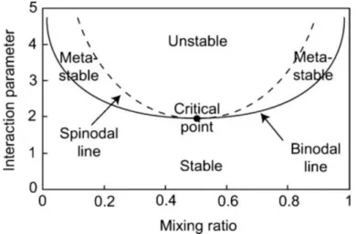
3.4. Mixing components 32
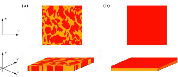
3.5. Phase segregation 34
3.6. Conclusions 36
xvii
CHAPTER 4. ORGANIC ELECTRONICS 39
4.1. Semiconductors in electronics 39
4.2. Field-effect transistors 40
4.2.1. Basic operation of an organic field-effect transistor 40
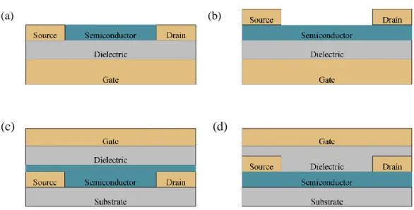
4.2.2. Field-effect transistor geometries 40
4.2.3. Measurement of electrical characteristics 42
4.2.4. Ambipolar field-effect transistors 44
4.2.5. Bias stress and current decay 44
4.2.6. Signal-to-noise ratio 46 4.2.7. Flexibility 47 4.3. Organic memories 48 4.3.1. Electrical programming 49 4.3.2. Photoprogramming 50 4.4. Conclusions 50 4.5. References 51
CHAPTER 5. EXPERIMENTAL TECHNIQUES 53
5.1. Device fabrication 53
5.1.1. Substrate preparation 53
5.1.1.1. Fraunhofer substrates 53
5.1.1.2. UV-Ozone cleaning 54
5.1.1.3. Polyethylene terephtalate substrates 54
5.1.1.4. Metal evaporation 55
5.1.1.5. Self-assembled monolayer treatments 57
5.1.2. Organic materials 57
5.1.2.1. Semiconductor and diarylethene solution preparation 57
5.1.2.2. Dielectric solution preparation 58
5.1.2.3. Solution deposition 58
5.2. Characterization techniques 59
5.2.1. Surface characterization 59
5.2.1.1. Atomic Force Microscopy 59
5.2.1.2. Mechanical contact profilometer 61
5.2.1.3. Contact angle 62
5.2.2. Ambient photoelectron spectroscopy 63
5.2.3. Electrical characterization 64
5.2.3.1. Probe-station 64
5.2.3.2. Light irradiation set-ups 65
CHAPTER 6. SOLUTION PROCESSED FIELD-EFFECT TRANSISTORS BASED ON OLIGOTHIOPHENE FILMS
WITH PERFORMANCES EXCEEDING THOSE OF VACUUM SUBLIMED FILMS 66
6.1. Introduction 66
6.2. Methods 67
6.2.1. Device fabrication 67
6.2.2. Device characterization 69
6.2.3. Atomic Force microscopy (AFM) 70
6.2.4. Ultraviolet photoelectron spectroscopy 70
6.3. DH4T transistors 70
6.4. Blends including DH4T 84
6.5. Conclusions 90
xviii
CHAPTER 7. AMBIPOLARITY ON DEMAND: POLYMER BLENDS 93
7.1. Introduction 93
7.2. Methods 95
7.2.1. Semiconductors 95
7.2.2. Fabrication of the devices 96
7.2.3. Device characterization 97
7.3. Single-component films 97
7.3.1. Energetic levels and electrical performances of the single polymers 97
7.3.2. Film morphology 101
7.4. Bi-component blends 103
7.4.1. Electrical performances of blends with different polymer-ratios 103 7.4.2. Correlation between molecular structure and electrical performances 106 7.4.3. Correlation between film morphology and electrical performances 107
7.4.3.1. Surface morphology 107
7.4.3.2. Top-gate transistors 109
7.4.3.3. Crystallinity 110
7.5. Conclusions 111
7.6. References 112
CHAPTER 8. OPTICAL MEMORY TFT DEVICE BASED ON AN ORGANIC BI-COMPONENT BLEND 114
8.1. Introduction 114
8.2. Methods 115
8.2.1. Transistors on SiO2 115
8.2.2. Transistors on PET 116
8.2.2.1. Top-gate transistors on PET 116
8.2.2.2. Bottom-gate transistors on PET, Cytop dielectric 117
8.2.2.3. Bottom-gate transistors on PET, PMMA-PVP dielectric 117
8.2.3. Device characterization 118
8.2.4. Illumination setups 119
8.3. Three-terminal memory devices on SiO2. 120
8.4. Switching with ultrafast light irradiation. 124
8.5. Three-terminal device memories on a flexible PET substrate. 126
8.5.1. Top-gate geometry 127 8.5.2. Bottom-gate geometry 129 8.6. Conclusions 133 8.7. References 134 CHAPTER 9. CONCLUSIONS 136 9.1. Conclusions 136 9.2. References 139 List of publications 140 List of Communications 140 Statement of work 141 Acknowledgements 142
xix
S
YMBOLS AND ABBREVIATIONS
AFM Atomic force microscopy
Ag Silver Au Gold C10 1-decanethiol CB Chlorobenzene CHCl3 Chloroform Ci Dielectric capacitance Cr Chrome DAE Diarylethene DAE-Me 1,2-Bis(2-methyl-5-p-tolylthiophen-3-yl)cyclopent-1-ene
DAE-Me_c DAE-Me in the closed form
DAE-Me_o DAE-Me in the open form
DCB 1,2-dichlorobenzene
DH2T Dihexylbithiophene
DH4T Dihexylquaterthiophene
DH6T Dihexylsexithiophene
DHnT Hexyl-terminated thiophene oligomers
Ɛ Permittivity e- Electron Ɛ0 Vacuum permittivity Ec Conduction band Ef Fermi level Eg Band gap Ɛr Relative permittivity Ev Valance band eV Electronvolt
Evac Vacuum level
FC10 1H,1H,2H,2H-perfluorodecanethiol
FET Field-effect transistor
GIXD Grazing incident X-ray diffraction
h+ Electron-hole
HMDS Hexamethyldisilazane
HOMO Highest occupied molecular orbital
IDS Drain-source current
IE ionization energy
IGS Leakage current
IIDDT-C3
poly[1,1'-bis(4-decyltetradecyl)-6-methyl-6'-(5'-methyl-[2,2'-bithiophen]-5-yl)-[3,3'-biindolinylidene]-2,2'-dione]
Ioff Lowest IDS value
Ion Highest IDS value
Ion/Ioff Ion-to-Ioff ratio
kB boltzman constant
L Channel length
LUMO Lowest unoccupied molecular orbital
MTR Multiple trap and release model
OFET Organic field-effect transistor
OM Optical microscopy
OTFT Organic thin-film transistor
xx
P Pressure P(NDI2OD-T2) Poly[N,N'-bis(2-octyldodecyl)-naphthalene-1,4,5,8- bis(dicarboximide)-2,6-diyl]-alt-5,5'-(2,2'-bithiophene) P3HT Poly (3-Hexylthiophene) PCD-TPT Poly4H-cyclopentadithiophenediyl) thiadiazolopyridinediyl(4,4-dihexadecyl-4H-cyclopentadithiophenediyl) PDVT-8 Poly[2,5-bis(2-octyldodecyl)pyrrolo[3,4-c]pyrrole-1,4(2H, 5H)-dione-alt 5,5′-di(thiophen-2-yl)-2,2′-(E)-2-(2-(thiophen-2-yl)vinyl)thiophene]PET Polyethylene terephthalate
PMMA Poly(methylmethacrylate)
PVP Poly(4-VinylPhenol)
Rchannel Channel resitance
Rcontact Contact resistance
RPM Rounds per minute
Rrms Root-mean-squared roughness
Rt Tunneling resistance
Rtotal Total resitance
SAM Self-assembled monolayer
Si Silicon
SiO2 Silicon dioxide
SNR Signal-to-noise ratio
T Temperature
TLM Transfer length method
ToF-SIMS Time of Flight Secondary Ion Mass Spectrometry
UPS Ultraviolet photoelectron spectroscopy
Vab Charge-transfer integral
VDS Drain-source voltage
VGS Gate-source voltage
VRH Variable range hopping
VTh Threshold voltage W Channel width W/L width-to-length ratio Wf Work function XRD X-ray diffraction α Tilt angle
ΔGevap Gibbs free energy of evaporation
ΔGl Molar Gibbs free energy (liquid)
ΔGm Gibbs free energy of mixing
ΔGv Molar Gibbs free energy (vapor)
ΔHm Enthalpy of mixing
ΔSm Entropy of mixing
λ Reorganizational energy
μ Field effect mobility
µeff Effective mobility
µn Electron field effect mobility
µp Hole field effect mobility
µp/µn p-type-to-n-type mobility ratio
τ Trapping time
τtr Average trapping time on shallow traps
φb. Schottky barrier
1
Chapter 1.
Introduction
1.1. Background
The blending of two materials in order to form a new one, with improved characteristics, is not a recent idea in human history. From artifacts produced from copper based alloys seven thousands of years ago 1 to modern polymer blends with improved thermal and mechanical properties, 2 blending has always been a go-to approach for many applications. Nevertheless, in the field of electronics, very pure single component materials are often privileged, due to their often superior performances, and addition of a secondary material is mostly limited to very small amounts, for doping purposes. 3-5 These inorganic electronic devices have demonstrated tremendous calculation capabilities, shaping the modern world. The first field-effect transistors, at the foundation of the logic gates necessary for data processing, were patented by Julius Edgar Lilienfeld first (in 1926) 6 and later by Oskar Heil in 1934, 7 but without any practical application. The first semiconducting devices were developed by the team of William Shockley at Bell Labs in 1947, opening the gates for an uninterrupted research in electronics, 8,9
with the first integrated circuit, developed by Jack Kilby, emerging in 1958. 10 Starting from less than ten transistors integrated in the early sixties, hundreds of millions of transistors now compose our processors, the central data processing units of our computers. As their power increased and their fabrication cost decreased, their potential for applications exploded, and microchips are now integrated in countless devices. From phones to tombstones, cars and pet-collars, everyday objects are transformed into controllable, connected, “smart” devices, which can collect and process data.
2
Unfortunately, electronics are still facing multiple limitations for future implementation. Silicon-based technologies tend to be very expensive and power consuming to produce, since microchips are fabricated on wafers grown from liquid silicon. Also, silicon-based chips are non-flexible and show no transparency. All these drawbacks have lead to parallel research on organic semiconductors as a replacement for inorganic technologies. The first field-effect transistor fabricated using an organic material as active semiconductor (polythiophene) was reported in 1987 by Koezuka and co-workers. 11 Since then, numerous polymers and small molecules based on thiophene units featuring semiconducting properties were synthetized, and viable organic field-effect transistors were fabricated. Novel materials integrating long conjugated systems with a wide variety of chemical functions were produced. Among them, some displayed all the characteristics lacking in their inorganic counterparts: flexibility, transparency, easily processing from the solution.
Regrettably, the “perfect” material has not emerged yet, each molecular material featuring very few strongly positive aspects, and a large variety of drawbacks such poor electrical performances, opacity, weak mechanical properties, air sensitivity or low solubility in the preferred solvents. While most of the research effort is still focused on the synthesis of novel materials, other approaches can lead to high-performing organic field-effect transistors. Two in particular stand out. First, the fabrication of the devices can be optimized, by careful selection of the processing techniques and consideration of the interfaces that determine the interplay between materials for improved electrical characteristics. Second, one particular strength of organic materials, the possibility to blend it in the solution, can be exploited. Two or more well established materials can be combined in the solution for the fabrication of devices with improved performances, and even completely new functions.
1.2. Aims of the thesis
While device optimization through developments of advanced processing techniques and tuning of injection barriers has always followed the study of organic materials, 12-14 blending organic materials for improved and new properties in electronics has only started to be thoroughly investigated since the mid-1990s. This approach yielded good results for augmentation of the electroluminescence of organic light emitting diodes and photovoltaics. 15-17 The concept was further extended to organic field-effect transistors with aims of improvement of electrical performances and implementation of novel features in organic devices. 18,19
In the work presented in this thesis, we will try to reach further in these directions and produce devices with the highest possible performances, using mostly small molecules and polymers available commercially. We will not limit ourselves to a single pair of molecules to be blended, but consider blends with sets of molecules that share similarities, in order to obtain a wider study that can be applied in multiple cases. We will consider blends composed of a family of small molecules
3
(oligothiophenes) in order to explore the consequences of the presence of similar molecules on the crystallinity and electrical performances of a semiconductor film. Films produced from polymer blends with radically different electrical characteristics and molecular structures for potential ambipolar transistors will be investigated. The presented work will be linked to real-world applications by the fabrication of a photoswitchable multilevel memory device based on a blend of a semiconducting polymer and a photochromic small molecule. We will aim to demonstrate the viability of such a technology by implementation onto a flexible substrate and measurement of long-term volatility.
In order to increase the performances of field-effect transistors produced from the solution, a large diversity of processing techniques have been developed, often by means of complex experimental setups (such as Langmuir Schaefer) that could not realistically be implemented into industrial applications. The works presented in this thesis will avoid such techniques and rely on simple processing of semiconducting materials that mimic industry-viable processes, such as ink-jet printing. Nevertheless, all transistors presented in this thesis will be fabricated upon careful investigation of the ideal interface tuning for optimal charge transport.
1.3. Structure of the Thesis
The thesis is composed of nine chapters. The work is arranged in the following order:
● Chapter 1 aimed to introduce the topic of the thesis and placed it in the scientific context. ● Chapter 2 will focus on charge transport in solid materials. It will try to provide a glimpse on
some theoretical aspects of charge transport in organic materials and charge injection across interfaces.
● Chapter 3 will present the materials employed in the thesis, their properties and characteristics. ● Chapter 4 will discuss organic field-effect transistors, their particular features and the their
electrical characterization.
● Chapter 5 will present the experimental techniques for device fabrication and the instruments used for sample characterization.
● Chapter 6 will focus on the optimization of films of dixehylquaterthiophene for improved electrical performances. It will focus on the control of the rate of evaporation and the functionalization of surfaces. It will explore the effect of blending of small semiconducting molecules for increased charge transport.
● Chapter 7 will center on a wide range of polymers with different electrical characteristics, blended for the fabrication of ambipolar transistors. It will demonstrate exceptional
4
performances for multiple polymer combinations. It will center on both electrical and morphological characterization in order to provide convincing explanations for the observed performances.
● Chapter 8 will spotlight field-effect transistors based on a polymer and a small photochromic molecule for photoswitchable memory applications. It will explore the fabrication and characterization of non-volatile multilevel memories with hundreds of discernible current levels. It will demonstrate the implementation of these devices on a transparent flexible polyethylene terephtalate substrate, and prove the ability to perform properly upon multiple bendings.
● Chapter 9, the conclusion, will summarize the work presented in the thesis, and give short term and long term outlooks.
1.4. References
1 Thornton, C. P., Lamberg-Karlovsky, C. C., Liezers, M. & Young, S. M. M. On pins and needles: Tracing the evolution of copper-base alloying at Tepe Yahya, Iran, via ICP-MS analysis of common-place items. J. Archaeol. Sci. 29, 1451-1460 (2002).
2 Utracki, L. A. & Wilkie, C. Polymer Blends Handbook. (Springer, 2010).
3 Zulehner, W. The Growth of Highly Pure Silicon-Crystals. Metrologia 31, 255-261 (1994).
4 Moskalyk, R. R. Gallium: the backbone of the electronics industry. Miner. Eng. 16, 921-929 (2003). 5 Jeon, H. G., Inoue, M., Hirarnatsu, N., Ichikawa, M. & Taniguchi, Y. A modified sublimation
purification system using arrays of partitions. Org. Electron. 9, 903-905 (2008).
6 Lilienfeld, J. E. Method and apparatus for controlling electric currents. U.S. patent (1926).
7 Heil, O. Improvements in or relating to Electrical Amplifiers and other Control Arrangements and Devices. U.K. patent (1934).
8 Bardeen, J. & Brattain, W. H. The Transistor, A Semi-Conductor Triode. Phys. Rev. 74, 230 (1948). 9 Shockley, W. & Pearson, G. L. Modulation of Conductance of Thin Films of Semi-Conductors by
Surface Charges. Phys. Rev., 232 (1948).
10 Kilby, J. S. Miniaturized Electronic Circuits. U.S. patent (1964).
11 Koezuka, H., Tsumura, A. & Ando, T. Field-Effect Transistor with Polythiophene Thin-Film. Synthetic. Met. 18, 699-704 (1987).
12 Law, K. Y. Organic Photoconductive Materials - Recent Trends and Developments. Chem. Rev. 93, 449-486 (1993).
13 Brown, A. R., Deleeuw, D. M., Lous, E. J. & Havinga, E. E. Organic N-Type Field-Effect Transistor. Synthetic. Met. 66, 257-261 (1994).
14 Katz, H. E. Organic molecular solids as thin film transistor semiconductors. J. Mater. Chem. 7, 369-376 (1997).
15 Park, J. Y. et al. The electroluminescent and photodiode device made of a polymer blend. Synthetic. Met. 79, 177-181 (1996).
16 Ferenczi, T. A. M. et al. Organic Semiconductor: Insulator Polymer Ternary Blends for Photovoltaics. Adv. Mater. 23, 4093 (2011).
17 Falke, S. M. et al. Coherent ultrafast charge transfer in an organic photovoltaic blend. Science 344, 1001-1005 (2014).
18 Park, B. et al. High-performance organic thin-film transistors with polymer-blended small-molecular semiconductor films, fabricated using a pre-metered coating process. J. Mater. Chem. 22, 5641-5646 (2012).
19 Lee, W. H. & Park, Y. D. Organic Semiconductor/Insulator Polymer Blends for High-Performance Organic Transistors. Polymers 6, 1057-1073 (2014).
6
Chapter 2.
Charge transport in organic materials
2.1. Introduction
This chapter will attempt to give a general overview on charge carriers and charge transport in on organic materials. It will discuss the presence of electrons in solids, and review the different types of materials depending on their energetic levels. It will consider the various interfaces between materials and how they affect charge carrier transport. In this chapter, we will also focus on the effect of impurities at the surface and within the materials. Finally, we will point out the optimal conditions for charge transport in organic materials.
2.2. Charges in materials
2.2.1. Energetic levels
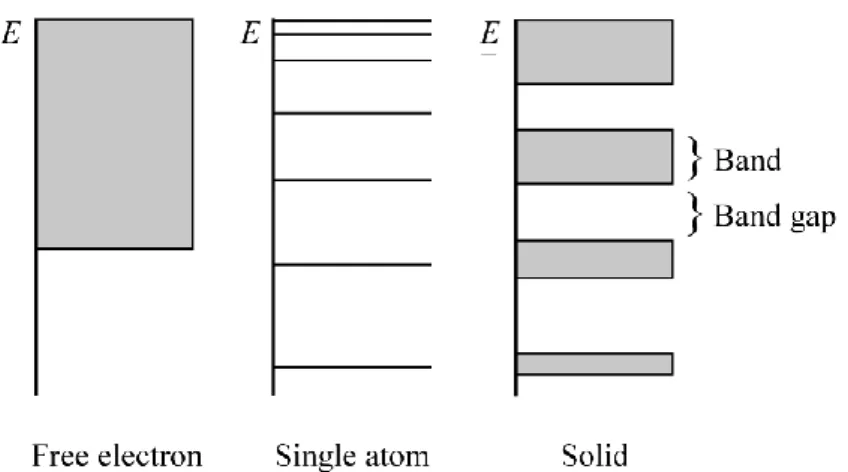
In the case of an electron not bound to an atom, such as a free electron in the gas phase, its energy is not limited to a strict value. 1 In an isolated atom, the energy of the electrons can only equal well defined discrete values, 2 which correspond to atomic orbitals. Any atom joining to form a molecule combines its atomic orbitals to form molecular orbitals, each of which equals a discrete energy level. 3 As more atoms are brought together, the molecular orbitals widen and their energetic levels form quasi-continuums instead of taking discrete values. These specific intervals where the energy of an electron can equal any value are represented as bands, and separated by band-gaps (Figure 2.1). 4 While the higher occupied energetic levels broaden into large energy-bands, the inner
7
atomic electrons do not interact significantly with neighboring atoms, and their energy levels stay very close to their original values.
Figure 2.1: Representation of the possible energetic levels of an electron in different states at 0 K.
The Fermi-Dirac distribution f(ϵ) describes the distribution of particles (electrons in our case) over the possible energy states of the system. 5 It describes the probability of an electron to occupy a state with the energy ϵ. It allows determination of the average number of electrons occupying the state:
Eq. 2.1
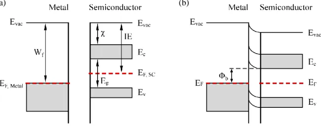
with T the temperature in K and kB the Boltzmann constant. The Fermi level, ϵ = EF, is defined as the level with 50% chance of occupancy as determined from the Fermi-Dirac distribution. The Fermi level is represented alongside the bands in energy diagrams, as to determine the occupancy of the bands. All bands with energies below the Fermi level are filled, while those above are unoccupied. The highest occupied band (immediately below EF) is named the valence band (Ev), while the lowest unoccupied band (immediately above EF) is referred to as the conduction band (Ec), as represented in Figure 2.2. If the Fermi level is located within a band, valence and conduction band are overlapping. The vacuum level is the energy of a free stationary electron that is outside of any material. The energy required to extract an electron from the valence band maximum to the vacuum level is the ionization energy (IE). 6
If the valence band and conduction band are overlapping, the IE corresponds to the energy required to extract an electron from the Fermi level to the vacuum level and is called the work function (Wf).
8
Figure 2.2: Representation of the valence and conduction bands for a Fermi level within a band gap.
2.2.2. Charges and charge transport
The absence of one electron in the valence band is commonly referred to as an electron hole, and will be will be mentioned as a “hole” during the whole thesis. Holes are generated when an electron leaves the valence band for the conduction band (electron-hole pair generation). 7 Holes differ greatly from electrons as electrons (e-) are negatively charged and holes (h+) positively charged. In order to be potentially mobile, electrons at the highest occupied energy level, EF, have to be able to access a slightly higher energy level to provide net motion in a particular direction. Conversely, holes are potentially mobile if they are able to access a lower energy level. In the case of a valence and conduction band overlap (absence of band gap Eg at the Fermi level), both electron and hole transport are easily achieved since the Fermi level is present inside the continuum of allowed energy levels. Materials offering this characteristic are conductive. If the Fermi level is within a broad band gap far from the valence and conduction bands, charges cannot move within the material that is an insulator. If the Fermi level is within a band gap, but close to either the valence or the conduction band, charge mobility is potentially reachable under specific conditions, and the material is a semiconductor (Figure 2.3). If the Fermi level is close to the conduction band, electrons are potentially mobile and the solid is an n-type semiconductor. Conversely, potential hole movement due to proximity of the Fermi level to the valence band is characteristic of a p-type semiconductor. 8