HAL Id: hal-01589258
https://hal.archives-ouvertes.fr/hal-01589258
Submitted on 11 Jul 2018HAL is a multi-disciplinary open access archive for the deposit and dissemination of sci-entific research documents, whether they are pub-lished or not. The documents may come from teaching and research institutions in France or abroad, or from public or private research centers.
L’archive ouverte pluridisciplinaire HAL, est destinée au dépôt et à la diffusion de documents scientifiques de niveau recherche, publiés ou non, émanant des établissements d’enseignement et de recherche français ou étrangers, des laboratoires publics ou privés.
Coupling Optical and Electrical Modelling for the study
of a-Si:H-based nanowire Array Solar Cells
Alexandra Levtchenko, Raphaël Lachaume, Jérôme Michallon, Stéphane
Collin, J Alvarez, Sylvain Le Gall, Zakaria Djebbour, Jean-Paul Kleider
To cite this version:
Alexandra Levtchenko, Raphaël Lachaume, Jérôme Michallon, Stéphane Collin, J Alvarez, et al.. Coupling Optical and Electrical Modelling for the study of a-Si:H-based nanowire Array Solar Cells. physica status solidi (c), Wiley, 2017, E-MRS 2017 Spring Meeting – Symposium E ; E-MRS 2017 Spring Meeting – Symposium N, 14 (10), pp.1700181. �10.1002/pssc.201700181�. �hal-01589258�
Coupling optical and electrical modelling for the study of
a-Si:H based nanowire array solar cells
Alexandra Levtchenko*,1, Raphaël Lachaume1,2, Jérôme Michallon1,2,3, Stéphane Collin3, José Alvarez1, Sylvain Le Gall1, Zakaria Djebbour1, and Jean-Paul Kleider1
1
GeePs (Laboratoire de Génie électrique et électronique de Paris), UMR CNRS 8507, CentraleSupélec, Univ. Paris-Sud, Université Paris-Saclay, Sorbonne Universités, UPMC Univ Paris 06, 3 & 11 rue Joliot-Curie, Plateau de Moulon 91192 Gif-sur-Yvette, France
2
Institut Photovoltaïque d’Ile-de-France (IPVF), 8 rue de la Renaissance, 92160 Antony, France 3
Centre de Nanosciences et de Nanotechnologies, CNRS, Univ. Paris-Sud, Université Paris-Saclay, C2N – Marcoussis, 91460 Marcoussis, France
Coupled optical/electrical simulations have been performed on a p-i-n radial nanowire arrays based on crystalline p-type silicon (c-Si) core/hydrogenated amorphous silicon (a-Si:H) shell heterojunction. Three-dimensional (3D) optical calculations based on Rigorous Coupled Wave Analysis (RCWA) are firstly performed and then coupled to a semiconductor device simulator that exploits the radial symmetry of the nanowires. By varying either the doping concentration of the c-Si core, or the work function of the Al-doped ZnO (AZO) back contact we can separate and originally highlight the contribution to the cells performance of the nanowires themselves (the radial junction) from the planar part in between the nanowires (the planar junction). We show that the short-circuit current density (Jsc) only depends on the doping of the c-Si core indicating
that it is mainly influenced by the radial junction. Whereas the open-circuit voltage (Voc) is strongly affected by the back contact conditions (AZO work function), revealing
an important impact of the interspacing between the nanowires on the characteristics of the entire nanowire array. We explain this strong influence of the back contact conditions by the fact that it determines the band-bending in the a-Si:H absorber shell touching the AZO, i.e. in the planar part. Therefore, it directly impacts the potential drop (Vbi) in the same area. For low work functions, the dark current density (Jdark) is
increased in the planar region, where Vbi is lower, which degrades the Voc of the entire
cell.
1 Introduction
Recently, many researches have been focused on the development of nanowire arrays for microelectronic and photovoltaic applications [1, 2]. In the context of photovoltaics, optical modelling has been used to demonstrate light absorption enhancement in nanowire arrays as compared with planar cells [3-5]. However, in order to reduce the costs of such a structure, a promising design would consist in a nanowire with a thin-film absorber. Experimentally, significant improvements of nanowire growth and material properties have been reported for radial heterojunctions based on thin c-Si cores and a-Si:H absorber shells [6-8]. However, to
determine their ideal design it is necessary to resort to numerical simulations. Previous modelling work focused either only on their optical light harvesting properties [7, 9, 10] or only on their electrical performance without taking into account the light enhancement effects of nanostructuration [11, 12]. Besides, a study of both optical and electrical properties of c-Si/a-Si:H radial heterojunctions has already been proposed for a c-Si absorber [13], therefore it is now mandatory to couple optical models to electrical simulations to assess the carrier collection efficiency of nanowires based on a-Si:H absorbers. In this study we first performed optical modelling to determine the photogeneration rate distribution in nanowires as well as the available photocurrent. Then the photogeneration was imported into a semiconductor device simulator [14] to show the impact on electrical performance of the planar junction located in the interspacing between nanowires.
2 Modelling methods 2.1 Simulated structure
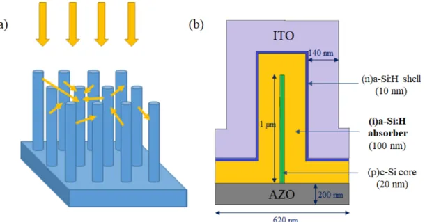
Figure 1 shows the structure of interest. The array of nanowires has been designed from experimental achievements [6-8]. For the modelling, a periodic square mesh arrangement was considered and the period was calculated from the density of nanowires determined by SEM
images for the best cell performance, namely 2.6 ×108 cm-2 (see Fig. 1a) [6] Each nanowire,
described in Fig. 1b, consists in a radial p-i-n junction with 20 nm p-type crystalline silicon core, (p)c-Si, covered by 100 nm of intrinsic hydrogenated amorphous silicon absorber, (i)a-Si:H, surrounded by n-type hydrogenated amorphous silicon shell, (n)a-Si:H of 10 nm. The 1 µm long (p)c-Si core allows the radial collection of holes which then flow to the back contact made of aluminium doped zinc oxide (AZO). Radial collection of electrons is ensured by indium tin oxyde (ITO). In addition to the radial junction of nanowires, there is a planar junction in between the nanowires for which the back contact acts as a hole collector.
2.2 Optical modelling
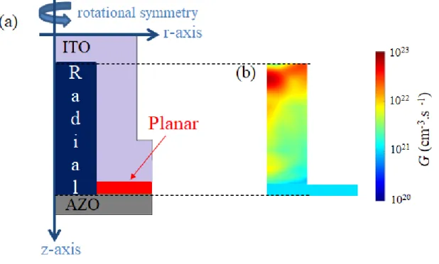
Photogeneration in the nanowire array was calculated with 3D Rigorous Coupled Wave Analysis (RCWA) method. Optical indices of materials were directly extracted from ellipsometry measurements. Photogeneration profile of a single nanowire is then extracted and flattened to a 2D plane. This photogeneration profile is then implemented into a semiconductor device simulator based on the finite volume method that exploits the radial symmetry of the nanowires (see Fig. 3).
2.3 Electrical modelling
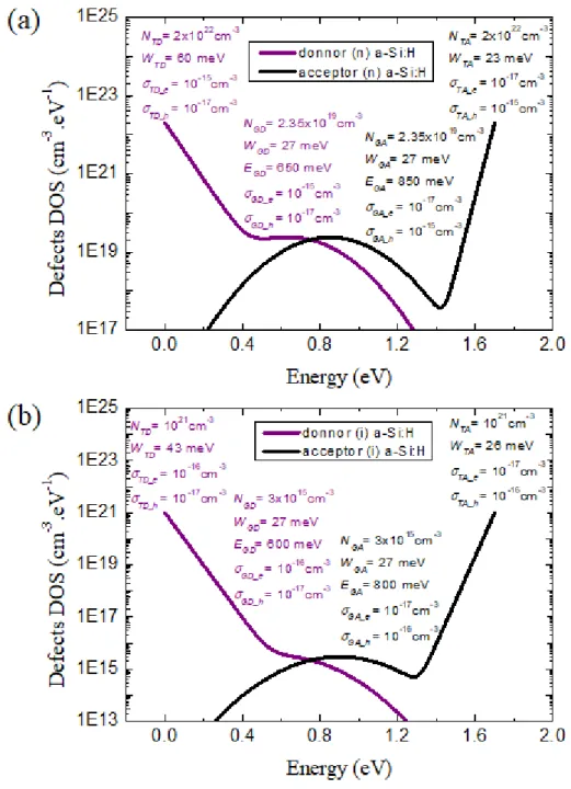
Electrical parameters of the materials are gathered in Table 1. Amorphous silicon was modelled with defects density of states (DOS) as described in Fig. 2a for (n)a-Si:H and 2b for
(i)a-Si:H. The doping of c-Si was varied in a large range: from 1017 to 8×1018 cm-3, while the
doping of (n)a-Si:H was set to 1.7×1019 cm-3 leading to a position of the fermi level of 0.16
eV under the conduction band with the introduced defects. The fermi level of (i)a-Si:H is located at 0.85 eV from the conduction band. The work function of ITO was chosen to meet flat band conditions at the ITO/(n)a-Si:H interface in order to study only the influence of the AZO contact. The reported work function of AZO depends on the measurement technique as well as on the material synthesis conditions [15], therefore in this study it was varied of ±500 meV around 5 eV. Interfaces between the different layers are considered ideal (no recombination). At the contacts, surface recombination velocities were taken infinite for both types of carriers as in [16].
3.1 Photogeneration and ideal current
Figure 3a shows the sketch of the electrically modelled structure (nanowire and the surrounding planar part) which takes into account the rotational symmetry of the nanowires around z-axis. The corresponding photogeneration rate (G) distribution, calculated by RCWA, is represented in Fig. 3b. It shows that in the designed array the light is mostly concentrated at
the top of the core of the nanowire. The resulting ideal current density (Jopt) corresponds to
the case in which all the photogenerated carriers are collected, and is expressed as:
𝐽𝑜𝑝𝑡 =𝑞.∭ 𝐺(𝑟,𝜃,𝑧).𝑑𝑟.𝑑𝜃.𝑑𝑧 𝑆 , (1)
where r, θ and z are respectively radial, angular and longitudinal components of cylindrical
coordinates, q is the electric charge and S is the area of a mesh, namely the square of the distance between two nanowires..
The global Jopt of the structure is 15.3 mA/cm². It is divided into 14 mA/cm² for the radial
part (91.5 %) and 1.3 mA/cm² for the planar part (8.5 %). 3.2 Carrier collection efficiency
When considering Jsc, modelling the planar part allows to take into account an
enhancement of 1.2 mA/cm² to the total Jsc thanks to its good carrier collection efficiency (Jsc
/Jopt) of 92.3 %. The nanowire part has also a good carrier collection efficiency (83.6 %)
meaning that the main way of improving the efficiency of the array is to optimize the absorption via the geometry of the nanostructuration and the optical properties of materials.
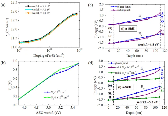
As shown in Fig. 3a, the studied structure has two types of junctions: a radial one in the nanowires, and a planar one related to the interspacing between these nanowires. The two parameters that influence their respective effects on the cell’s performance are the doping of the c-Si core and the back contact (AZO) work function, as they determine the band-bending in the absorber material (i)a-Si:H.
Figure 4a shows the short-circuit current density (Jsc) as a function of doping
concentration of c-Si for three different work function values. We notice a strong dependence on the doping of c-Si while it only slightly depends on the AZO work function. The major
increase of Jsc with doping occurs between 5×1017 cm-3 and 5×1018 cm-3 with an enhancement
of 11%. Then it saturates at a value of 12.9 mA/cm² for the best case. This harvesting can be explained by the increase of the electric field in both junctions: when the doping of (p)c-Si, or the AZO work function, increases the band-bending in the absorber gets stronger, resulting in a larger electric field. However, as the photogeneration rate in the radial part is much more important than in the planar one, there is a larger possibility of carrier collection enhancement by field effect there.
The work function of AZO has a strong impact on the open-circuit voltage as shown in Fig. 4b. This is also due to the variations of the band-bending in (i)a-Si:H. Figures 4c and 4d depict the 1D electronic band diagrams of both planar (r-axis cutline on Fig. 3a) and radial (z-axis cutline on Fig. 3a) junctions for work function values of 4.8 eV and 5.2 eV, respectively. The blue curve with circle markers and the green one with square markers correspond to the planar junction : (n)a-Si:H/(i)a-Si:H/AZO, while the purple curve with triangle markers corresponds to the radial one: (n)a-Si:H/(i)a-Si:H/(p)c-Si. It is important to notice that the
potential drop, or built-in potential (Vbi), in the absorber is different for each junction. When
Vbi is larger in the radial part (see Fig. 4c), namely for work functions up to 5 eV, Voc depends
only on the planar junction contact. When Vbi is lower in the radial part (see Fig. 4d), Voc also
depends on the radial contact.
𝑉𝑜𝑐 = 𝑛𝑘𝑇𝑞 ln �𝐽𝑑𝑎𝑟𝑘𝐽𝑠𝑐 �, (2)
where n is the ideality factor of the diode, k is the Boltzmann constant, T is the temperature, q is the electric charge, Jsc the short-circuit current density, and Jdark the current density in the
dark. Considering that Jsc does not vary consequently with the AZO work function, as shown
in Fig. 4a, the variations of Voc directly depend on those of Jdark. When increasing the work
function, Jdark also rises as depicted in Fig. 5a. When looking at the distribution of Jdark at Voc
(i.e. for the same total current density value) at different work functions (see Fig. 5b, 5c and
5d) it appears that it increases in the planar region when its Vbi is smaller than the radial one.
It then starts to flow to the radial junction when increasing the work function, therefore making the planar region more resistive.
Depending on the structure’s parameters, the planar junction can drastically affect the
performance of the full cell: for low work functions, the planar region degrades the Voc of the
entire cell.
4 Conclusions
In this paper we performed coupled optical/electrical modelling of c-Si core / a-Si absorber-shell radial heterojunction nanowires array. We showed the importance to take into account the region between the nanowires as it consists in a planar junction which influences the performance of the entire cell. The efficiency is determined by the work function of the
back contact through the Voc which is degraded when the dark current density is concentrated
in the planar region.
Acknowledgements
This work has been supported by the French Research National Agency – project SOLARIUM (ANR-14-CE05-0025).
References
[1] K.-Q. Peng and S.-T. Lee, Advanced Materials 23, 198 (2011).
[2] N. P. Dasgupta, J. Sun, C. Liu, S. Brittman, S. C. Andrews, J. Lim, H. Gao, R. Yan, and P. Yang, Advanced Materials 26, 2137 (2014).
[3] M. Foldyna, L. Yu, and P. Roca i Cabarrocas, Solar Energy Materials and Solar Cells 117, 645 (2013).
[4] J. Michallon, D. Bucci, A. Morand, M. Zanuccoli, V. Consonni, and A. Kaminski-Cachopo, Optics Express 22, A1174 (2014).
[5] J. Lu, S. Qian, Z. Yu, S. Misra, L. Yu, J. Xu, Y. Shi, P. Roca i Cabarrocas, and K. Chen, Optics Express 23, A1288 (2015).
[6] S. Misra, L. Yu, M. Foldyna, and P. Roca i Cabarrocas, Solar Energy Materials and Solar Cells 118, 90 (2013).
[7] S. Misra, L. Yu, M. Foldyna, and P. Roca i Cabarrocas, IEEE Journal of Photovoltaics 5, 40 (2015).
[8] S. Misra, M. Foldyna, I. Florea, L. Yu, and P. Roca i Cabarrocas, MRS Proceedings 1770, 73 (2015).
[9] L. Yu, S. Misra, J. Wang, S. Qian, M. Foldyna, J. Xu, Y. Shi, E. Johnson, and P. Roca i Cabarrocas, Scientific Reports 4, 4357 (2014).
[10] S. Qian, S. Misra, J. Lu, Z. Yu, L. Yu, J. Xu, J. Wang, L. Xu, Y. Shi, K. Chen, and P.
Roca i Cabarrocas, Applied Physics Letters 107, 043902 (2015).
[11] Zingway Pei, Shu-Tong Chang, Chang-Wei Liu, and Yi-Chan Chen, IEEE Electron Device Letters 30, 1305 (2009).
[12] D. Diouf, I. Ngo, J.-P. Kleider, M. Gueunier-Farret, and J. Alvarez, Physica Status Solidi (a) 209, 1026 (2012).
[13] M. Zanuccoli, I. Semenihin, J. Michallon, E. Sangiorgi, and C. Fiegna, Journal of Computational Electronics 12, 572 (2013).
[14] User’s manual for ATLAS from Silvaco International
[15] R. Jaramillo and S. Ramanathan, Solar Energy Materials and Solar Cells 95, 602 (2011).
[16] R. Lachaume, W. Favre, P. Scheiblin, X. Garros, N. Nguyen, J. Coignus, D. Munoz,
Figure 1 (a) Geometry of the simulated nanowire array. (b) Detailed structure of a single nanowire and the planar junction interspacing that has been modelled.
(p) c-Si (i) a-Si:H (n) a-Si:H
Eg (eV) 1.12 1.7 1.7 χ (eV) 4.05 3.8 3.8 εr 11.9 11.9 11.9 µn (cm²/(V.s)) 1300 20 20 µp (cm²/(V.s)) 491 4 4 Nc (cm-3) 2.8×10¹⁹ 5×10²⁰ 5×10²⁰ Nv (cm-3) 1.04×10¹⁹ 5×10²⁰ 5×10²⁰
Figure 3 (a) Sketch of the radial symmetry of nanowires with the surrounding planar part. (b)
Figure 4 Parameters influencing Jsc and Voc. (a) Variation of the short-circuit current density
(Jsc) as a function of doping concentration of c-Si for three different work function values
(black square symbol: 5.5eV; blue line: 5.2 eV and orange triangle: 4.8 eV). (b) Open-circuit
voltage (Voc) as a function of AZO work function for two doping concentration values (blue
star: 1×1018 cm-3 and green cross: 8×1018 cm-3). (c) and (d) represent the 1D band diagrams of both junctions for respectively AZO work function of 4.8 eV (c) and 5.2 eV (d). The blue curve with circle markers and the green one with square markers correspond to the planar junction : (n)a-Si:H/(i)a-Si:H/AZO, while the purple curve with triangle markers corresponds to the radial one: (n)a-Si:H/(i)a-Si:H/(p)c-Si.
Figure 5 (a) Dark current density dependence on bias for Na=8×1018 cm-3. Map of Jdark
distribution in the entire structure at Voc for different AZO workfunctions (b) 4.8 eV, (c) 5.0

![[PDF] Formation informatique Xhtml en pdf](data:image/gif;base64,R0lGODlhAQABAIAAAP///wAAACH5BAEAAAAALAAAAAABAAEAAAICRAEAOw==)