HAL Id: hal-01233039
https://hal.archives-ouvertes.fr/hal-01233039
Submitted on 23 Dec 2015HAL is a multi-disciplinary open access
archive for the deposit and dissemination of sci-entific research documents, whether they are pub-lished or not. The documents may come from teaching and research institutions in France or abroad, or from public or private research centers.
L’archive ouverte pluridisciplinaire HAL, est destinée au dépôt et à la diffusion de documents scientifiques de niveau recherche, publiés ou non, émanant des établissements d’enseignement et de recherche français ou étrangers, des laboratoires publics ou privés.
Design challenges of EO polymer based leaky waveguide
deflector for 40 Gs/s all-optical analog-to-digital
converters
Massinissa Hadjloum, Mohammed El Gibari, Hong Wu Li, Afshin S. Daryoush
To cite this version:
Massinissa Hadjloum, Mohammed El Gibari, Hong Wu Li, Afshin S. Daryoush. Design challenges of EO polymer based leaky waveguide deflector for 40 Gs/s all-optical analog-to-digital converters. Optics Communications, Elsevier, 2016, 373, pp.82-90. �10.1016/j.optcom.2015.10.009�. �hal-01233039�
Design Challenges of EO Polymer Based Leaky
Waveguide Deflector for 40 Gs/s All-Optical
Analog-to-Digital Converters
Massinissa Hadjloum
a*, Mohammed El Gibari
a, Hongwu Li
a, Afshin S.
Daryoush
ba Lunam Université, Université de Nantes, UMR CNRS 6164: Institut d'Electronique et de Télécommunications de Rennes,
Faculté des Sciences et Techniques, 2 Chemin de la Houssinière, BP 92208, 44322 Nantes cedex 3, France
b Dept. of ECE, Drexel University, Philadelphia, PA 19104, USA
*Corresponding author. Tel.: 00 33 251125535. E-mail address: massinissa.hadjloum@univ-nantes.fr
Abstract
Design challenges and performance optimization of an all-optical analog-to-digital converter (AOADC) is presented here. The paper addresses both microwave and optical design of a leaky waveguide optical deflector using electro-optic (E-O) polymer. The optical deflector converts magnitude variation of the applied RF voltage into variation of deflection angle out of a leaky waveguide optical beam using the linear E-O effect (Pockels effect) as part of the E-O polymer based optical waveguide. This variation of deflection angle as result of the applied RF signal is then quantized using optical windows followed by an array of high-speed photodetectors. We optimized the leakage coefficient of the leaky waveguide and its physical length to achieve the best trade-off between bandwidth and the deflected optical beam resolution, by improving the phase velocity matching between lightwave and microwave on one hand and using pre-emphasis technique to compensate for the RF signal attenuation on the other hand. In addition, for ease of access from both optical and RF perspective, a via-hole less broad bandwidth transition is designed between coplanar pads and coupled microstrip (CPW-CMS) driving electrodes. With the best reported E-O coefficient of 350 pm/V, the designed E-O deflector should allow an AOADC operating over 44 giga-samples-per-seconds with an estimated effective resolution of 6.5 bits on RF signals with Nyquist bandwidth of 22 GHz. The overall DC power consumption of all components used in this AOADC is of order of 4W and is dominated by power consumption in the power amplifier to generate a 20V RF voltage in 50Ohm system. A higher sampling rate can be achieved at similar bits of resolution by interleaving a number of this elementary AOADC at the expense of a higher power consumption.
Keywords: All-optical analog-to-digital converter; Leaky waveguide deflector; Electro-optic polymer; GCPW-CMS transitions; Pre-emphasis technique, Effective number of bits, Spatial filter.
1. Introduction
High speed analog-to-digital converters (ADCs) are key components for enhancing high speed communications systems, such as broadband satellites at millimeter wave frequencies [1] and extremely high-throughput wireless systems [2]. Tens of gigahertz ADCs are required to cope with the increasing need of real time digital signal processing (DSP) of broad bandwidth analog RF signal in direct digital receivers. However, electronic ADCs have inherent difficulties in reaching high bandwidth with appropriate resolution [3] because of timing jitters of the electronic clocks. The real-time oscilloscope LabMaster 10 Zi-A built by LeCroy is claimed to have until 100-GHz bandwidth with a 240 GS/s sampling rate [4]; however, all real-time oscilloscopes operating over 10 GHz currently are based on multiple interleaved ADC that employs a lower sampling rate ADC [5] as their elementary unit ADC. In the same way, 56-GS/s 8-bit ADC by Fujitsu is built with 320 interleaved 175-MS/s 8-bit ADCs [6]. Interleaving is a very attractive and efficient technique to increase sampling rate and could in principle be applied to many ADC even though it results in a higher complexity, more noise, and high power-consumption for the same effective number of bits (ENoB). The interleaved ADC suffer from matching problems in time between each interleaved elementary ADCs; moreover, K. Poulton [7] predicted that not all ADCs could be interleaved and Rohde & Schwarz opted to develop a single flash ADC with 8 bits of resolution that samples at 10 GS/s and 7 ENoB in its R&S@RTO Series real-time oscilloscopes
[8]. According to the latest survey of the ADC performances in July 2015 by Murmann [9], the fastest single-channel flash ADC was reported by W. Cheng et al. [10] and it operates with direct conversion rate up to 40 GS/s but only 3 bits resolution. The targeted performance of AOADC presented in this paper is with a sampling rate of 44 GS/s and a 6.5 bits resolution that results in a resolution-sampling rate product of 3.98×10¹² LSBs-Hz, which is an order of magnitude higher than the fastest
single-channel electronic flash ADCs with 3.2×10¹¹ LSBs-Hz. Current research on electric ADCs focuses on reduction of
power consumption and active area [11]. Optical ADCs take advantage of much lower optical clock jitters available from mode-locked laser (MLL) to achieve tens of giga-samples-per-second (GSPS) rates with high resolution by avoiding the aperture jitter limits of the electronic ADC. All-optical ADCs (AOADCs) perform both sampling and quantization in optical domain, as opposed to hybrid ADCs where usually sampling is done in optical domain and quantization in electrical domain [12]. The AOADC reported in this paper operates in spatial domain, using an electro-optic (E-O) polymer based leaky waveguide deflector, by converting magnitude of input analog voltage into angular displacement of a leaky optical beam. The amount of deflected optical beam power impinging on each optical window is the same for each applied RF voltage level and results in the same amplitude for each digitized bit; hence, it does not suffer from quantization errors observed in other ADC. The AOADC is designed to operate at Nyquist sampling rate of 40 GSPS with effective number of bit resolution of over 6.5 bits (i.e., 90 quantization levels), on instantaneous signal bandwidth of 22 GHz.
E-O polymers based leaky waveguide deflectors are selected over E-O crystals because of its ultra high-speed operation, a better phase velocity matching between travelling optical and electric waves due to a smaller difference in index of refraction at RF and optical frequencies, and manufacturing compatibility with Si-Photonics. RF bandwidth of 110 GHz is demonstrated for stabile E-O polymer based optical Mach-Zehnder (MZ) modulators [13]. In addition, the progress in chromophore synthesis and high efficiency poling allow obtaining polymers with E-O coefficient up to 350 pm/V [14], while the E-O coefficient of the widely used inorganic crystals in commercial MZ modulators, such as LiNbO3, is only 31 pm/V.
The operation principle of the AOADC is explained in the Section 2, while the Section 3 addresses bandwidth optimization by improving velocity matching between microwave and optical wave and resolution optimization by compensating for the RF electric field attenuation using pre-emphasis filtering of CMS electrodes. Finally, the via hole free back-to-back GCPW-CMS-GCPW microwave transitions from external RF coaxial probe transition to planar transmission lines are presented in the Section 4 that results in both velocity matching and uniform RF field distribution along the optical waveguide.
2. Principle of AOADC using leaky waveguide E-O deflector
Figure 1 depicts the principle of the spatial-sampling AOADC based on leaky waveguide E-O deflector, where short optical pulses at GSPS rates from MLL are being spatially deflected using an E-O polymer based leaky waveguide deflector, and quantization is attained by illuminating the deflected optical pulses on an spatial optical filter that is realized based on a selected binary coding mask. The short optical pulses samples the applied RF signal by deflecting the light in the E-O polymer based optical deflector and then passed through optical windows, which are used for quantization by detecting deflected light beam using an array (e.g., 8x3 for a 3bit quantizer) of ultra high-speed photodetectors. The MLL generates short pulses of the order of picoseconds and of timing jitters below 100 fs at repetition rate of over 40 GHz to achieve Nyquist sampling of 40 GSPS for an RF signal with a maximum bandwidth of 20 GHz. The minimum required optical power of MLL is about 15mW with DC and drive RF mode-locking power consumption of under 100mW [15]. The E-O deflector steers the optical beam from the MLL into a direction according to the magnitude of the RF signal.
The optical waveguide deflector converts the RF voltage variation into angular deflection angles of the leaky beam; therefore, the position of each sampling pulse on the coding mask varies as a function of the magnitude of the applied RF analog signal. Low speed (sub-milliseconds) optical deflectors have been developed for optical scanners, laser printers, and photocopiers, but the leaky optical waveguide deflector is designed for a very high-speed (sub-nanoseconds) operation. In fact, the leaky waveguide deflector with sub-nanoseconds deflection speeds is a critical component of this proposed GSPS AOADC, where its RF bandwidth determines the Nyquist sampling bandwidth. Moreover, the diffracted optical beamwidth and the maximum optical deflection angle of this optical deflector define the effective number of bits of this spatial sampling AOADC. These features make the design aspects of optical deflector somewhat challenging.
The quantization of the proposed AOADC is based on optical spatial filtering using a coding mask, as depicted in Figure 1. The apertures of the optical spatial filter collect the angular information by an array of photodetectors mounted behind the array of apertures. High-speed photodectetors of RF bandwidth above 20 GHz are necessary for quantizing the sampled RF signal at the MLL wavelengths. The binary decisions of logics “0” and “1” for each aperture corresponding to a given bit is performed after the photodetection of the deflected short optical pulses across an array of optical spatial filter apertures. For a 7 bit AOADC, a 128x7 array of photodetectors are required. When the deflection angle points to a specific row of photodetectors, then the binary on or off optical window pattern quantizes the RF signal. The logic bit "1" (e.g., a photocurrent of about mA for about mW optical power out of optical deflector) is considered when the detected photocurrent is above a set threshold (e.g., about 10A) and logic bit "0" (e.g., dark reverse channel current of 100nA) is set to be well below threshold well below (e.g., about 10A). In addition to the binary coding masks, the Gray coding masks could also be realized to improve accuracy of quantization process by changing the distribution of the optical windows across photodetector array.
3. Geometry and design of leaky waveguide deflector
Physical geometry of the E-O polymer based optical deflected is depicted in Figure 2. In the design and performance simulation of this optical deflector, three-dimensional (3D) optical modeling is performed using beam propagation method (BPM) in the integrated optics simulator of OptiBPM, a commercial CAD tool developed by Optiwave Systems Inc. The BPM solver employs finite difference solution of Maxwell’s equations in place of partial derivatives and it is a computationally intensive program that accurately calculates a very wide range of optical devices. A commercial CAD tool developed by Ansys Inc, High Frequency Structure Simulator, is employed for full wave microwave modeling of E-O deflector. The numerical simulation and design optimization is performed by solving Maxwell’s equations at discrete nodal points on tetrahedron meshes using the finite element method (FEM).
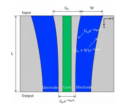
Fig. 2 :The optical leaky waveguide deflector on silicon wafer. (a) Cross section. (b) Longitudinal section.
The leaky waveguide deflector of the AOADC has a structure similar to that of a conventional optical phase modulators, except that the top cladding (buffer layer) is thin enough and covered by a prism-superstrate (cf. Figure 2), whose refractive index ns is greater than the effective index neff of the waveguide. The applied RF signal causes change in index of refraction of
the E-O polymer based optical waveguide and hence changes the refracted wave angle. Nonetheless, tail of the optical field extends into the superstrate due to dispersion relationship of waves in the optical waveguide of substrate and superstrate. Since normal component of the wave Poynting vector in superstrate has a real part, then energy leaks out of the optical waveguide from superstrate, while the wave vector also propagates along the longitudinal direction of the optical waveguide, as depicted in Figure 2b.
The modulation bandwidth and resolution of the AOADC is sensitive to the thickness of the buffer layer hb, index of
refraction difference between core and cladding regions of optical waveguide, and the material absorption losses at optical and microwave frequencies.
Since a multi-mode waveguide deflector would lead to broadening of the leaked out optical beam, then the leaky waveguide deflector requires remaining single-mode for a narrow optical beamwidth that leads to a high-resolution AOADC. In fact in leaky waveguide supporting multiple modes, every mode corresponds to a different effective index, and consequently every mode leaks at different angle θ (cf. shown in Figure 2b) determined using Snell-Descartes’ law of refraction:
sin
θ
=(
n
eff/
n
s)
(1)Single-mode operation of optical waveguides at a given operating wavelength critically depends on the waveguide dimensions and the index contrast between the core and the upper and lower claddings. Several criteria must be considered when choosing the cladding material. First of all, its refractive index must be lower than that of the core E-O polymer but should have an appropriate value. In fact, high index contrast allows reducing the driving voltage by reducing the gap G between electrodes (cf. Figure 2.a). However, too high contrast index involves a small core section, thus resulting in lower light confinement factor . In addition, the cladding material must be chemically and thermally compatible with the core E-O polymer.
In order to realize a realisticlly high-performance AOADC that is based on leaky waveguide deflector, we assume the polymer used as core material has an E-O coefficient of 350 pm/V, as reported by Huang et al. [14]. Unfortunately the microwave and optical characteristics of this polymer is not reported in [14], hence the design is based known polymer PMMI (e.g., a host matrix polymer for the chromophore reported in [16]) to emulate an optical deflector realized using the-state-of-art E–O coefficient of 350 pm/V. The refractive index of the E–O polymer is nc=1.63 with dielectric constant of εc=3.15. Lower cladding and buffer layer are with refractive index of ng=nb=1.56 and dielectric constant of εc=εb=3.2 (i.e., typical values for NOA63 polymer), and superstrate is in glass with ns=1.7 and εs=5. All refractive indices values are considered at center wavelength of about λ0 = 1550 nm and the single-mode operation of the leaky optical waveguide is achieved with 1.8 µm x 1.8
µm cross-section for the square optical core. When short optical pulses from the MLL are provided using single mode optical fiber to the optical deflector, the square cross section provides a 71% light confinement in the core region and is better mode matched with spherical lensed single mode optical fibers than the rectangular waveguides.
The width f of the sidewalls between metallic RF electrodes and optical core (cf. Figure 2a) has an impact on both light confinement and electric field for a given applied RF voltage. If distance f is too short, the optical field would not decay enough at the sidewall/electrode interfaces and lightwave would experience additional Ohmic losses due to finite conductivity of metallic electrodes; while a large separation of f results in a higher gap, G, between two coupled strips since G = a + 2f. A larger gap leads to a higher RF voltage for a required electric field and associated deflection angle of the leaky waveguide per Eq. 1. A design compromise is made between these two limiting factors of applied voltage and lightwave confinement with selection of f = 1.2 µm, where for a gap of G = 4.2 µm the optical intensity decays below 1 % at the sidewall/electrode interfaces.
The effective index achieved is neff = 1.5882 with the selected material properties and dimensions, giving rise to a leaky angle
θ = 1.2061 radian (or 69°) in absence of E-O effect (VRF = 0 V). When a RF voltage is applied, a variation of the effective index
is induced via Pockels effect of
Δn
eff(
z)=
1
2
n
eff03
r
eo
ΓE(z )
, where E(z) is the electrical field along the propagation axisat the position z,
Γ
is the overlap between electrical and optical fields,n
eff0 is the effective index when VRF = 0 V andr
eo is the electro-optic coefficient. The resulting effective index in the core is hence expressed as:n
eff=
n
effo+
Δn
eff=
n
effo+
1
2
n
eff03
r
eoΓE(z)
(2)This index variation modifies leaky lightwave direction by Δθ, which can be expressed from derivative of θ with respect to neff in
relation (1) by:
∆ θ=
∆ n
effn
scos θ
=
n
eff0 3r
eoΓE(z )
2 n
scos θ
(3)Equation (3) demonstrates that the angular sweep Δθ is proportional to the applied electric field E(z); therefore, the input RF voltage is linearly mapped into angular deflection of optical beam.
3.1. Bandwidth consideration of leaky waveguide deflector
The leaky waveguide deflector should been designed to obtain the best possible velocity matching between optical and electrical waves, so each optical pulse is “accompanied” by the same traveling electric field to experience the same induced E-O effect along the waveguide at all applied RF frequencies. The velocity mismatch of the E-O deflector limits the modulation bandwidth since the modulation bandwidth is inversely proportional to [17]:
∆ f =
2 c
π
|
n
eff−
√
ε
RF|
L
(4)where c is the speed of light in free space, L is the length of the optical deflector, and εRF is the microwave effective dielectric
constant. The silicon substrate for the E-O deflector is selected for its low cost integration with RF electronics circuits, good flatness, stiffness, and capability being cleaved following an accurate direction since light injection requires good input waveguide facets, but the high dielectric constant silicon wafer (εSi = 11.9) will undoubtedly slows down the RF signal
propagation wave velocity. Therefore, in order to eliminate velocity mismatch caused by high dielectric constant of silicon wafer, a metallic ground plane is set between silicon wafer and lower cladding (in NOA63) to screen the silicon as depicted in Figure 2a. The metallic screen thus isolates the RF electric field from Si substrate, which permits to reduce considerably effective permittivity of εRF, down to 3.6 instead of 6.4 in absence of metallic ground plane. As result of a better velocity
matching due to ground plane shielding, the modulation bandwidth consequently increases from 10.1 GHz to 30.9 GHz for an E-O deflector of length L = 2 cm.
The velocity matching will not only improve the optical deflector bandwidth, but also its resolution, as the reduction in the timing jitters of MLL optical pulses and any excessive microwave attenuation. Indeed, a better velocity matching will allow a longer length for the optical deflector waveguide, which results in a narrower beamwidth; moreover, the leaky lightwave will be focused on even finer line due to constructive interference between in-phase elementary leaky optical fields generated along the waveguide. The narrower optical beamwidth increases the number of resolvable lines (i.e., quantization levels) focused on the coding mask and therefore improving the effective number of resolution bits of the AOADC. However, RF attenuations should be reduced to maintain a uniform RF electric field across the optical waveguide and maximize its resolution by using a longer optical deflector waveguide. To achieve this performance improvement, we present an original pre-emphasis technique to compensate the RF attenuation in the following sub-section.
3.2. Leaky wave divergence angle of δθ in lossy RF transmission lines
The number of resolved lines on the coding mask N is given by the following formula:
N= Δ/δθ
(5)where Δθ is the total angular deflection swing according to the Eq. (3) and δθ is the divergence angle of leakage beam. The number of resolution bits b=log2N. As the electro-optic coefficient of the E-O polymer enhances a larger
Δ
is obtained andthe diffraction angle
δθ
decreases as a longer optical deflector is employed.However, the leaky beam divergence δθ depends upon lightwave attenuation coefficient
α
opt
, leakage coefficientαleak
, length of the optical waveguide L due to diffraction, and RF attenuation coefficientα
RF . Particularly, different deflectionangles are caused by different E-O effect over the waveguide length according to Eq. (1) and Eq. (2). The total angular deflection swing Δ of the deflected beam is proportional to both maximum voltage swing of the RF signal and the E-O coefficient of polymer. For a given Δθ of the deflected beam, one should reduce the leaky beam divergence to increase the resolution, so the effective leaky waveguide length Leff must be close to L, thus ensuring a small leaky wave beamwidth from
optical diffraction. A weak leaky wave condition can be achieved by controlling the leaky coefficient αleak, which varies
depending on index contrast
∆ n=n
c−
n
b and the thickness of the buffer layer,h
b . Figure 3a renders the influence ofh
b onα
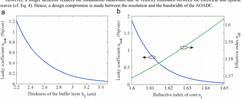
leak , where a thicker buffer layer results in a smaller leaky wave coefficient. For a smaller leaky waveguidecoefficient the optical wave travels a longer distance over the optical waveguide and results in a smaller optical beamwidth for the diffracted beam, as the wave exits prism superstrate.
However, a longer deflector reduces the modulation bandwidth due to velocity mismatch between the electrical and optical waves (cf. Eq. 4). Hence, a design compromise is made between the resolution and the bandwidth of the AOADC.
Fig. 3 : (a) Influen ce of the buffer layer thickness on the leaky wave coefficient with core of side a=1.8 µm and refractive index nc=1.63 and lower cladding and buffer layer refractive index ng=nb=1.56 at wavelength λ0=1.55 µm. (b) Influence of the refractive index of core on leaky
wave coefficient with buffer layer thickness of hb=2.9 µm.
Many types of polymer materials with high E-O coefficient can be used for core of the E-O deflector. Their refractive indices range generally between 1.60 and 1.65. The dependency of the leaky coefficient on the refractive index of core E-O material is depicted as solid line in Figure 3b. Leaky coefficient drops with increasing index contrast between the core and the buffer layer as the optical wave is confined more in the core of the waveguide with a higher index contrast. This reduction in the optical field into the prism superstrate results in a reduced optical leakage coefficient. The effective index increases with core index as shown by the dashed lines in Figure 3b. When the materials of the E-O deflector are selected, one can adjust the leaky coefficient at will by choosing an appropriate buffer layer thickness.
By summing the contribution at each segment dz of the waveguide to the optical leaky wave and taking into account optical and RF losses, the total leaky lightwave
ψ
at the deflection angle θ is given by the following integral:ψ=α
leakA e
−j ksr∫
0
L
exp
{
[
−
(
α
leak+
α
opt)
−
j
(
β−k
ssin θ
)
]
z
}
dz
, (6)where A is the magnitude of the input lightwave in the waveguide at the origin z = 0, β = kneff is the phase constant of the
lightwave in the waveguide, where
k =2 π / λ
0 is the optical wavenumber in free space;α
opt is the total optical lossescaused by material absorption and waveguide imperfection (roughness in particular). Note that Eo is the magnitude of the RF
field at the input port of the coupled microstrip (CMS) electrodes, and r is a position in superstrate. The phase propagation constant
β
can be expressed as a function of the longitudinal position z and the RF attenuation coefficientα
RF as:β=k
(
n
effo+
1
2
n
3 eff0r
eoΓ E
oe
−αRFz)
(7)By incorporating Eq. (7) into Eq. (6), the total leaky optical field at the deflection angle θ is then rewritten in the following integral:
ψ =α
leakA e
−j ksr∫
0
L
exp
{
[
−
(
α
leak+
α
opt)
−
j
(
β −k
ssin θ
)
]
z
}
dz
(8) The influence of various parameters on the resolution has been studied with the help of Eq. (8) and numerically calculated (cf. Figure 4) using the mathematical program Matlab. The peak in Figure 4a corresponds to the normalized optical intensity of the leaky lightwave in function of output beam angle θ without any E-O effect, when VRF= 0 V. This result has been obtainedFor a small value of the leaky coefficient αleak, typically comprised between 0.1 and 0.2 Np/cm, optical losses have a little
impact on the divergence δθ of leaky beam. The high leakage coefficient leads to a larger diffracted optical beam divergence angle as the effective waveguide length Leff is reduced (cf. Figure 4b). Any increase of optical losses results also in an increase
of the beam divergence via reduction of the effective waveguide length. Optical losses can be further mitigated by choosing a small leaky coefficient.
Fig. 4 : (a) Normalized intensity of the optical leaky wave in function of output beam angle θ when leaky coefficient is αleak=0.1 Np/cm, effective index of neff0neff0=1.5882, waveguide length of L=2 cm and electrical field E0=0; (b) Influence of the leaky coefficient αleak on beam divergence δθ.
Microwave attenuation degrades the resolution of an AOADC based on leaky waveguide deflector by angular broadening the optical leaky beam (i.e., making optical beam more divergent), as shown in Figure 5. If microwave losses are negligible by setting αRF=0 in the term
e
−j 1
2k neffo
3 r
eoΓ Eoe
−αRFzz
of Eq. (8), then the leaky beams throughout the interaction length L arrive in phase at the prism and air interface of superstrate. This deflected output beams are focused at the output of the E-O deflector using a cylindrical lens. The contributions of deflected beam are added by constructive interference of the leaky wave along length L, which results in a narrow beam represented by the peak in solid line in Figure 5. The peak beamwidth is only limited by diffraction. However, in reality, microwave losses are never null and cause enlargement of the leaky beam because the electrical field reduces over the waveguide length, so both the phase and the deflection direction of elementary leaky optical fields change from a point to another along the waveguide axis. When focused by the cylindrical lens, the local leaky beams are added with different phase shifts, giving rise to an enlarged main peak with the secondary peaks depicted in dashed line in Figure 5. This broadening of the leaky wave beamwidth is more pronounced with increasing waveguide length L due to the none-negligible RF losses. We overcome the RF propagation losses using a pre-emphasis technique.
Fig. 5: Influence of microwave losses on the beam divergence δθ. Results obtained with leaky coefficient
αleak=0.2 Np/cm, effective index neff0neff0=1.5882, waveguide length L=3 cm and RF voltage VRF=10 V.
3.3 Pre-emphasis filter design of the electric field
Since RF voltage applied between the two strips decays exponentially along the propagation axis z, electric field decays also exponentially along the propagation axis z. The RF electric field along with a constant gap G0 in a classical CMS electrode:
E
(
z
)
=
V
RF(
z )
G
0=
V
oe
−αRFzG
0 (9)To negate any electric field decay, it is proposed to design a pre-emphasis filter by exponentially reducing the gap between the two strips along the axis z, as shown in Figure 6. Conceptually this change in gap is equivalent to mathematically multiply the denominator in Eq. (9) by the factor
e
−αgapz as expressed by:E=
V
RF(
z)
G(z )
=
V
0e
−αgapzG
0e
−αRFz=
V
0G
0e
(αRF−αgap)z (10)Fig. 6 : Modified CMS strips shape and gap to pre-emphasize the electric field along the propagation direction z.
Therefore, the pre-emphasized E field will be uniform, when
α
gap=
α
RF . To keep the characteristic impedance matched toHowever, microwave losses increase with frequency, as shown in Figure 7, the bandwidth is limited over which the compensation improves significantly the E-O deflector performances. Indeed, when the compensation is performed at a given frequency fc, electric field is slightly magnified at lower frequencies (f < fc) thus still causing variation of electric field. The
frequency where exact compensation is made (i. e. αgap = αRF(fc)) must be chosen as a compromise between significant
improvement at the high frequencies (i.e., f > fc) and small distortions at the lower frequencies (i.e., f < fc), according to
frequency range for which resolution improvement is looked for by the pre-emphasis filtering method.
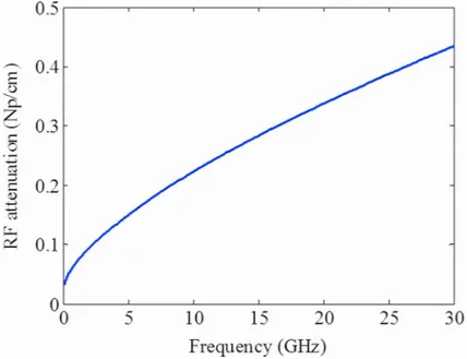
Fig. 7 : RF attenuations coefficient in the E–O deflector made with polymers PMMI (tangent loss of ε″/ε′=10−3) as core material and NOA65 or NOA73 (tangent loss of ε″/ε′ =2.2×10⁻²) as cladding and buffer material, superstrate in glass (ε″/ε′=10−5) and electrodes in copper (electrical conductivity of σ=5.8×10⁷ S/m) for CMS strips.
With the microwave properties of the polymers PMMI (tangent loss of ε″/ε′=10−3) as core material, NOA63 or NOA73 (tangent loss of ε″/ε′=2.2×10−2) as cladding and buffer material, superstrate prism in glass (ε″/ε′=10−5), and CMS strips electrodes using copper (electrical conductivity of σ = 5.8x10⁷ S/m), the RF attenuation coefficient α
RF as frequency function is plotted in Figure
7. These polymers are chosen for leaky waveguide deflector due to their good index contrast (nc = 1.63 vs ng = nb = 1.56), low
material loss tangent, and good mechanical adhesion.
Figure 8a displays the simulated magnitude of electric field in the optical core center at the frequencies 5, 10 and 20 GHz for constant strips width W = 50 µm and gap G0 = 4.2 µm along the z axis. These curves show an exponential decay of the electric
field intensity throughout z axis, which causes of the leaky wave beamwidth broadening as displayed by dashed lines in Figure 5. The reason for this broadening of beamwidth is due to changing of both phase and local direction of leaky optical field from one point to another over the waveguide length.
Figure 8b shows the magnitude of electric field, for the frequencies 5, 10 and 20 GHz in center of the optical core, when the gap between the two strips decay exponentially with a decay coefficient αgap= 0.22 Np/cm for 10 GHz frequency (or 1.91 dB/cm,
cf. Figure 7). The resulting electric field in the core region is constant over the waveguide length at the frequencies around 10 GHz, slowly decaying at 20 GHz (0.058 Np/cm) and weakly enhanced at 5 GHz (0.040 Np/cm). This compensation allows limiting to a very small level the electric field variation in the frequency band from 5 up to 20 GHz, which reduces considerably the divergence of leaky beam δθ as explained before. Therefore, thispre-emphasis improves the achieved effective resolution bits of the designed AOADC.
3.4. Total angular sweep of Δθ
In Figure 9a renders plot the two deflected beam peaks corresponding respectively to maximum applied voltages VRF = ±20V.
The spacing between them corresponds to the total angular sweep Δθ. This result has been obtained using Eq. (8) with waveguide length L = 3cm, optical losses αopt = 0.345 Np/cm, RF losses αRF = 0.01 Np/cm (after RF attenuation compensation
technique described in Section 3.3). A leaky coefficient αleak = 0.10 Np/cm, E-O coefficient reo = 350 pm/V, and gap between the
two strips at the waveguide input side Go = 4.2 µm are also employed with an overlap integral Г = 100 % between the RF and
optical fields.
Fig. 9 : Simulation results obtained with Eq. (8) with L=3 cm, αopt=0.345 Np/cm, αRF=0.01 Np/cm (after RF attenuation compensation),
αleak=0.1 Np/cm, Г =100%, VRF=± 20 V and gap between strips G0=4.2 µm. (a) Leaky intensity peaks for applied voltages V=−20 and +20 V and reo=350 pm/V. (b) Number of resolved lines on the coding mask versus E–O coefficient.
The dashed line in Figure 9b shows that when electric field attenuation is zero, the resolution is proportional to both E-O coefficient and the applied electric field. Therefore, the output angle displacement varies linearly with the applied RF voltage, so the applied voltage is linearly translated into angular displacement in the spatial domain. However under the above conditions, when considering non-zero attenuation, as shown by solid line in Figure 9b, resolution N remains proportional to the E-O coefficient for values up to 200 pm/V. The resolution reaches an optimum value of about 73 quantization levels for 240 pm/V and then decreases beyond that level because of leaky beam angular enlargement due to interference between phase-shifted elementary leaky optical fields generated along the waveguide caused by electric field variation. In such a case, then we should reduce leaky waveguide length to achieve a higher resolution by minimizing overall phase-shift induced interference along the optical waveguide.
3.5. Optimal length of the leaky waveguide deflector
The divergence angle of the deflected optical beam from the leaky waveguide is limited by two main factors: i) diffraction, which its impact is weakened when increasing waveguide length L; and ii) deflection angle dispersion of the leaky wave beamwidth due to the RF field attenuation, whose the effect is increased with a longer waveguide. Actually, with short leaky waveguide, electric field variation is still small and its influence is negligible compared to diffraction effect, and therefore, in this range of length (L < 2 cm for reo = 350 pm/V) resolvable lines number increases proportionally with length L, as shown in
Figure 10. However depending on the strength of E-O coefficient, diffraction influence and electric field attenuation are reversed after optical deflector length of about 2 cm. The optimal length L is 2 cm for an E-O polymer with reo = 350 pm/V, as
shown in Figure 10, leading to N = 90 lines, which corresponds to 6.5, as the effective number of bits.
Fig. 10 : Number of quantization levels (resolved lines on coding mask) versus leaky waveguide deflector length with VRF=±20 V,
αleak=0.1 Np/cm, αRF=0.01 Np/cm, αopt=0.345 Np/cm and reo=350 pm/V.
4. Microwave accesses of the E-O deflector
Using the realized travelling wave configuration with characteristic impedance of Zo, the E-O deflector must be excited by RF
matched source and load impedances of ZS and ZL respectively. The CMS line is designed for impedance matching to Zo = ZS =
ZL = 50 Ω and on the other hand, for velocity-matching between microwave and optical wave allowing operation bandwidth of
over 30 GHz. The achieved characteristic impedance of Zo depends not only on the geometric parameters of the CMS line, but
also on all the surrounding materials. The gap G between CMS electrodes is fixed by optical core width and sidewalls width. Manufacturing of core and electrodes channels can be made using reactive ion etching (RIE), which is the most common method for fabrication of the optical waveguides.
Both connectorized and on-wafer characterization of the E-O deflector require coplanar (CPW) microwave interconnects or the use of GSG (Ground-Signal-Ground) probes from a probe station to assure reliable electrical contacts that is compatible with coplanar transmission lines. A transition between coplanar and coupled microstrip line (CPW-CMS) is thus required to characterize components driven by the CMS line with the CPW probe station.
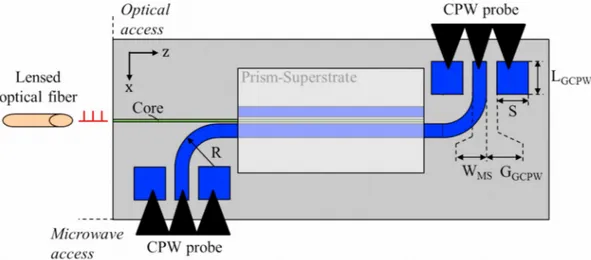
In the designed E-O deflector, both the optical waveguide core (with square side of a = 1.8 µm) and the traveling wave electrodes (separated by gap of 4.2 µm at the input side) are in the same xz plane, as shown by the cross section in Figure 2a. Compared with the case, where optical core is below the strips [18], this configuration allows better optical and electrical waves overlap, Γ. In fact a Γ = 61% instead of 40% as estimated in the last design. In addition, this configuration reduces the number of technological steps by manufacturing both core and strips channels at the same technological step. However, coupling of the optical pluses from the MLL into the optical waveguide core and applying a microwave signal onto electrodes by the same side is not feasible because of mechanical limitations of accommodating both optical fiber (diameter of ~ 120 µm) and probe head (~ 3 mm). It's then necessary to bend the electrodes away from the optical input for separating the optical access points from the microwave access points, as illustrated in Figure 11. Optical access is feasible because of constraints related to dimensions of optical core.
Nevertheless, a direct CPW-CMS transition (all strips in the same level) would make one ground strip of the CMS line intersect with the optical waveguide core, which is obviously unacceptable. Our solution consists of making a virtually grounded at RF frequencies by capacitive effect of the lateral ground pads of the input GCPW section with the bottom ground plane; and then have the bottom ground plane capacitively coupled with the ground strip of the CMS line (cf. Figure 11). In this topology the electromagnetic energy is first transferred from the input GCPW section to the bent MS line section (GCPW-MS) then from the bent MS section to the CMS line (MS-CMS).
Fig. 11: Diagram of the via-free transitions permitting applying electrical voltage to the CMS electrodes without intersecting E–O leaky waveguide.
We present in this section design and performance prediction of a back-to-back GCPW-CMS-GCPW transition for feeding the E-O deflector (cf. Figure 11) with the CPW probes. The E-O deflector is located in the CMS section of the transition. Built on an optimum thin substrate (lower cladding in Fig. 2a) of hg=20 µm in NOA63 (ε′=3.2 and ε″/ε′=0.022) to realize velocity-matching (cf. sub-section 3.1). As both the GCPW and MS sections are built in 20 µm NOA65 polymer and the CMS section in NOA65 and PMMI E-O polymer, we use the software Linecalc from the Agilent’s Advanced Design System (ADS) to determine the strip width in MS section and the gap in GCPW section for matching their characteristic impedances Zo_MS and
Zo_GCPW to 50 Ω. In CMS section, iterative HFSS simulations are performed to determine optimum CMS strips width W0 from
the gap G0 = 4.2 µm at the input side chosen in section 3 for a lower cladding thickness hg = 20 µm and buffer layer thickness hb
= 3.2 (for αleak = 0.1 Np/cm) in NOA63 and the superstrate thickness hsup of a few centimeters in glass.
Parasitic resonances in the GCPW structures were analyzed in [19], while studying GCPW-MS-GCPW transitions bandwidth. Energy in GCPW line can propagate into three modes owing to the bottom ground plane: in addition to the MS and CPW modes, a coplanar microstrip mode (CPM) is excited between bottom ground plane and coplanar pads, causing energy to escape from the CPW mode and giving rise to resonance peaks in the insertion loss plot of S21-parameter curve (cf. Figure 11). Low
effective permittivity εRF pushes parasitic resonances to very high frequencies, according to Eq. (11) giving their approximate
resonance frequencies using cavity model equation [20]:
f
mn=
c
2
√
ε
g[
(
m
S
)
2+
(
n
L
GCPW)
2]
1/ 2 (11)where S and LGCPW are GCPW ground pads width and length, as shown in Figure 11,
ε
g is relative permittivity of lowercladding, m and n are the mode integers. Parameters S and LGCPW determine parasitic peaks frequency on |S21|-parameter curve;
in addition, they have an important influence on low cut-off frequency of the bandwidth. Indeed, pad surface areas of A = S·LGCPW determines capacitive effect between CPW pads and full plate bottom ground plane. To reduce the lower cut-off
frequency as small as possible without affecting significantly the higher cut-off frequency, the width and length of pads are optimized to S = LGCPW = 1 mm, so CPW mode can be stabilized and converted to MS mode in the bent section of the MS line.
Figure 12 presents microwave bandwidth of designed E-O deflector including the via-free GCPW-CMS-GCPW transition (cf. Figure 11). According to these results, E-O deflector can operate over the frequency range from 1.5 to 22.3 GHz. Due to the capacitive effect, this transition has a high upper cut-off frequency (22.3 GHz for an E-O deflector of length L = 2 cm) and is easy to realize (without holes and without pattering bottom ground plane) resulting in a lower manufacturing cost over a via-hole based structures. However, this solution doesn’t allow digitizing RF signals below 1.5 GHz due to a high insertion loss of the E-O deflector (cf. Figure 12). Via-holes can be made between top ground pads of the GCPW line and bottom ground plane to enable a low-pass operation up to 22.3GHz.
Fig. 12 : S21 and S11 parameters for CMS section of length L=2 cm.
5. Conclusions
Design of a leaky waveguide deflector is presented in this paper for implementation of a 44GSPS AOADC. The design of leaky waveguide deflector is based on low RF loss material with optical loss of αopt < 0.345 Np/cm and high E-O coefficient
reo=350 pm/V to achieve 6.5 effective bits of resolution. An optimum leaky waveguide deflector length of L=2 cm and
pre-emphasis technique allowing compensation of RF wave losses. Broad bandwidth up to 22.3 GHz is reached due to a good velocity matching between microwave and band GCPW-CMS-GCPW transition is discussed with a bandwidth of 1.5 to 22.3 GHz for applying RF signal to the E-O deflector, while providing access for the lensed fiber optical input from a MLL. The DC power consumption of this AOAD is dominated by the 4W consumed in a 50 Ohm load as result of providing a sinusoidal peak RF voltage of 20V to the CMS electrodes of the E-O deflector. A100% efficiency is theoretically possible, when the Class C power amplifiers are employed, while the Class B push-pull power amplifiers with 78% efficiency are also feasible, resulting still under 5W of total power consumption. The other sources of power consumption are less significant compared to the power amplifier and the optical deflector, as the reported optical sampler uses under 100mW for clock and optical output power of 30mW using low jitters optical clocks from the MLL. In addition a 7 bit optical quantizer consumes under 50mW, when only one row of 7 photodetectors out of 128 x 7 photodetector array are being illuminated by about 5mW of deflected optical beam impinges on to the optical windows. The future EO material improvements to the anticipated level of 1200pm/V will undoubtedly lower the required RF voltage and result in a power consumption of about 0.5W, while it provides sampling rate over 44 GSPS with resolution of approaching 8 bits.
Acknowledgement
The authors would like to thank the Region of Pays de la Loire for its support through the project ADC PolyNano. Moreover, the authors greatly appreciated numerous discussions and helpful recommendations by Prof. Gundel, Prof. Guiffard and Dr Ginestar on practical implementation of EO-Polymer based leaky waveguide optical deflector in the project.
References
[1] A. S. Daryoush, X. Hou, W. Rosen, All-optical ADC and its applications in future communication satellites, IEEE International Topical Meeting on Microwave Photonics, (2004), 182-185.
[2] L. Verma, M. Fakharzadeh, S. Choi, WiFi on Steroids: 802.11ac and 802.11ad, IEEE Wireless Communications, (2013), pp. 30-35.
[3] M. El-Chammas, B. Murmann, A 12-GS/s 81-mW 5-bit Time-Interleaved Flash ADC With Background Timing Skew Calibration, IEEE Journal of Solid-State Circuits, 46(4), (2011), 838-847.
[4] http://cdn.teledynelecroy.com/files/pdf/labmaster-10zi-a-datasheet.pdf
[5] P. J. Pupalaikis, B. Yamrone, R. Delbue, A. S. Khanna, K. Doshi, B. Bhat, and A. Sureka, Technologies for Very High Bandwidth Real-time Oscilloscopes, invited lecture to IEEE Bipolar/BiCMOS Circuits and Technology Meeting (BCTM 2014), 128-135.
[6] P Bower, and I Dedic, High speed converters and DSP for 100G and beyond, Optical Fiber Technology, (2011), 467-471. [7] K. Plouton, Time-Interleaved ADCs, Past and Future, IEEE International Solid State Circuits Conference, Feb 10, 2009. [8] Rohde & Schwarz, Oscilloscope Fundamentals, 2014. Available :
https://www.conres.com/test-equipment/wp-content/uploads/sites/4/2014/04/oscilloscopefundamentals.pdf.
[9] B. Murmann. ADC performance survey 1997-2015 (July 2015). [Online]. Available: http://web.stanford.edu/~murmann/adcsurvey.html
[10] W. Cheng, W. Ali, M.-J. Choi, K. Liu, T. Tat, D. Devendorf, L. Linder, and Ronald Stevens, A 3b 40GS/s ADC-DAC in 0.12µm SiGe, IEEE International Solid-State Circuits Conference (2004), 262-263.
[11] J.-H. Tsai, H.-H. Wang, Y.-C. Yen, C.-M. Lai, Y.-J. Chen, P.-C. Huang, P.-H. Hsieh, H. Chen, and C.-C. Lee, A 0.003 mm2
10 b 240 MSPs 0.7 mW SAR ADC in 28 nm CMOS With Digital Error Correction and Correlated-Reversed Switching, IEEE Journal of Solid-State Circuits 50(6), (2004), 1382-1398.
[12] Y. Han, B. Jalali, Photonic Time-Stretched Analog-to-Digital Converter: Fundamental Concepts and Practical Considerations, IEEE Journal of Lightwave Technology, 21(12), (2003), 3085-3103.
[13]D. Chen, H. R. Fetterman, A. Chen, W. H. Steier, L. R. Dalton, W. Wang, Y. Shi, Demonstration of 110 GHz electro-optic polymer modulators, Applied Physics Letters, 70(25), (1997), 3335-3337.
[14] S. Huang, T.-D. Kim, J. Luo, S. K. Hau, Z. Shi, X.-H. Zhou, H.-L. Yip, A. K.-Y. Jen, Highly efficient electro-optic polymers through improved poling using a thin TiO2-modified transparent electrode, Applied Physics Letters, 96(24), (2010), 243311:1-3.
[15] S. Arahira, N. Mineo, K. Tachibana, and Y. Ogawa, 40 GHz hybrid mode-locked laser diode module operated at ultra-low RF power with impedance-matching circuit, Electron. Lett., vol. 39, no. 3, pp. 287–289, 2003.
[16] X. Wang, C.-Y. Lin, S. Chakravarty, J. Luo, A. K.-Y. Jen, R. T. Chen, Effective in-device r33 of 735 pm/V on electro-optic
polymer infiltrated silicon photonic crystal slot waveguides, Opt. Lett., 36(6), (2012), pp. 882–884.
[17] B. M. A. Rahman, V. Haxha, S. Haxha, K. T. V. Grattan, Design optimization of polymer electrooptic modulators, Journal of Lightwave Technology, 24(9), (2006), 3506-3513.
[18] X. Hou, A Leaky Waveguide All-Optical Analog-to-Digital Converter, PhD Thesis, Drexel University, Pheladelphia, PA, 2004.
[19]J.-P. Raskin, G. Gauthier, L. P. Katehi, G. M. Rebeiz, Mode conversion at GCPW-to-microstrip-line transitions, IEEE Transaction On Microwave Theory and Techniques, 48(1), (2000) 158-161.
[20] W. H. Haydl, On the use of vias in conductor-backed coplanar circuits, IEEE Transaction On Microwave Theory and Techniques, 50(6), (2002), 1571–1577.