HAL Id: tel-03041538
https://tel.archives-ouvertes.fr/tel-03041538
Submitted on 5 Dec 2020HAL is a multi-disciplinary open access
archive for the deposit and dissemination of sci-entific research documents, whether they are pub-lished or not. The documents may come from teaching and research institutions in France or abroad, or from public or private research centers.
L’archive ouverte pluridisciplinaire HAL, est destinée au dépôt et à la diffusion de documents scientifiques de niveau recherche, publiés ou non, émanant des établissements d’enseignement et de recherche français ou étrangers, des laboratoires publics ou privés.
Mechanism of spin-orbit torques in platinum oxide
systems
Jayshankar Nath
To cite this version:
Jayshankar Nath. Mechanism of spin-orbit torques in platinum oxide systems. Materials Science [cond-mat.mtrl-sci]. Université Grenoble Alpes, 2019. English. �NNT : 2019GREAY067�. �tel-03041538�
Pour obtenir le grade de
DOCTEUR DE LA COMMUNAUTÉ
UNIVERSITÉ GRENOBLE ALPES
Spécialité : Physique de la Matière Condensée et du
Rayonnement
Arrêté ministériel : 25 mai 2016
Présentée par
Jayshankar NATH
Thèse dirigée par Gilles GAUDIN et codirigée par Ioan Mihai MIRON
préparée au sein du Laboratoire Spintronique et Technologie
des Composants (SPINTEC)
dans l'École Doctorale Physique
Mécanisme des Couples Spin-Orbite
dans les Systèmes à l'Oxyde de Platine
Mechanism of Spin-Orbit Torques in
Platinum Oxide Systems
Thèse soutenue publiquement le 5 Décembre 2019, devant le jury composé de :
M. Mairbek CHSHIEV
Professeur, SPINTEC/Université Grenoble Alpes, Président
M. Felix CASANOVA
Directeur de Recherche, CIC nanoGUNE, Rapporteur
M. Michel VIRET
Cadre Scientifique des EPIC, SPEC/CEA, Rapporteur
M. Mihai GABOR
Maître de Conférence, Université Technique de Cluj-Napoca, Examinateur
i
Résumé de la Thèse
Mécanisme des Couples Spin-Orbite dans les Systèmes à l'Oxyde de Platine
par
Jayshankar NATH Doctorat en Physique Université Grenoble Alpes, 2019 Dr. Gilles GAUDIN, Directeur de Thèse Dr. Mihai MIRON, Co-Directeur de Thèse
L'avènement du Big Data, Machine Learning (ML) et 5G a l’importance de certains paramètres clé des technologies mémoire tels que la consommation d'énergie, la non-volatilité, la vitesse, la taille et l'endurance. Les mémoires magnétiques à accès aléatoire (MRAM) telles que les MRAM à couple de transfert de spin (STT-MRAM) et les MRAM à couple de spin orbite (SOT-MRAM) sont devenues des concurrents incontournables de ce marché, dans l’objectif d’remplacer les RAM statiques (SRAM) et les RAM dynamiques (DRAM) actuelles basées sur la technologie CMOS (Complementary Metal-Oxide-Semiconductor). La commutation d’un bit mémoire dans les SOT-MRAMs s'appuie sur les spins générés via le couplage spin orbite (SOC) par l'application d'un courant de charge à travers un métal lourds (HM). Ces HM étant résistifs, des pertes ohmiques existent pendant le processus d'écriture. Un vaste corpus de travaux, tant universitaires qu'industriels, a été consacré à la recherche de moyens pour minimiser ces pertes et ainsi améliorer l'efficacité énergétique. De plus, le courant injecté dans la mémoire lors du processus d'écriture est contrôlé par un transistor de commutation CMOS. La taille de ce transistor augmente avec le courant de commutation. Par conséquent, une réduction de ce courant conduit également à un gain de densité de la mémoire.
Diverses approches visant à améliorer la génération de spins par unité de courant appliqué ont été adoptées pour atteindre cet objectif. Les premières ont consist à utiliser des métaux de transition présentant un SOC élevé, des alliages métalliques et/ou une phase structurelle résistive du métal. Des travaux plus récents se sont concentrés sur l'ingénierie de l’interface : insertion de couches ultrafines et utilisation de couches de capping formant des puits de spin. L'une des approches actuelles concerne l'utilisation de l'oxydation comme moyen d'augmenter les SOT. Différents groupes ont étudié l'effet de l'oxydation du HM, du Ferro-Magnétique (FM) ainsi que de la couche de capping constituée de métaux plus légers comme le cuivre. Bien que la majorité de ces travaux fass état d'une augmentation des SOT, les résultats et les conclusions ne sont pas cohérents. Des tendances divergentes d'augmentation des SOT, qui ont, à leur tour, été attribuées à des phénomènes physiques variés. Dans
ii
ce travail, nous étudions les SOTs générés par l'oxydation de la couche de platine dans une pile multicouche Ta/Cu/Co/Pt.
Dans ce système, nous quantifions les SOTs en mesurant les couples par une technique de seconde harmonique. Nous observons en effet une augmentation des couples. Ceci est vérifié par des mesures de spin pumping qui montrent une augmentation de l'amortissement. Afin de déterminer l'origine de cette augmentation, nous avons construit un modèle décrivant l'oxydation du système basé sur des caractérisations électriques, magnétiques et matérielles ansi que des calculs ab-initio de la théorie fonctionnelle de la densité (DFT). Ceci nous a conduit à la conclusion que contrairement aux travaux précédents, qui expliquaient les résultats en se basant exclusivement sur un modèle où seul le HM était oxydé, dans la pratique l'oxygène près de l'interface FM/HM est pompé dans la couche FM. Ce phénomènz ne conduit pas seulement à une oxydation FM, mais laisse aussi le HM métallique à proximité de l'interface. En outre, ce modèle a été étayé par des mesures et des calculs des échanges symétrique et anti-symétrique. En tenant compte de ces observations et une fois les SOT quantifiés corrigés, nous ne constatons aucune augmentation observable des couples. Ceci nous amène à conclure que bien qu'au niveau du système il y ait une augmentation des SOTs avec l’oxydation du platine, il n'y a pas de contribution intrinsèque de l'oxyde de platine à l'augmentation des couples. Cette découverte a de vastes conséquences sur la conception de SOT-MRAM, affectant l'endurance, la consommation d'énergie et la magnéto-résistance tunnel (TMR).
Mots-clé: Couples de spin orbite (SOT), Mémoire magnétique à accès aléatoire (MRAM), Platine, Oxyde
iii
Abstract of the Thesis
Mechanism of Spin-Orbit Torquesin Platinum Oxide Systems
by
Jayshankar NATH Doctor of Philosophy in Physics Université Grenoble Alpes, 2019 Dr. Gilles GAUDIN, Thesis Director Dr. Mihai MIRON, Thesis Co-Director
The advent of Big Data, Machine Learning (ML) and 5G has placed a greater emphasis on certain key metrics of memory technology such as power consumption, non-volatility, speed, size, and endurance. Magnetic Random-Access Memories (MRAM) such as Spin Transfer Torque MRAM (STT-MRAM) and Spin-Orbit Torque MRAM (SOT-MRAM) have emerged as key contenders in this market, targeted towards replacing the current Complementary Metal-Oxide-Semiconductor (CMOS) based Static RAMs (SRAM) and Dynamic RAMs (DRAM). SOT-MRAMs rely on spins generated by applying a charge current through a metal with a high Spin-Orbit Coupling (SOC) to switch the magnetic memory bit. These Heavy Metals (HM) being resistive, lead to Ohmic losses during the write process. A vast body of work, both academic and industrial, has been dedicated to finding ways to minimize these losses and thereby enhance the energy efficiency. Moreover, the current that is injected into the device during the write process is controlled by a CMOS switching transistor. The size of this transistor increases with the switching current. Hence, a reduction in this current can also lead to a gain in the bit density of the memory.
Various approaches have been adopted to achieve this target by means of enhancing the generation of spins per unit applied current. The earliest approaches involved using transition metals with high SOC, metallic alloys and resistive structural phase of the metal. More recent works have focused on interfacial engineering via ultra-thin insertion layers and spin-sink capping materials. One of the current focus is on using oxidation as a means of enhancing the SOTs. Different groups have studied the effect of oxidation of the HM, the Ferro-Magnet (FM) as well as the capping layer consisting of lighter metals such as copper. Although majority of these works report an increase of SOTs in general, the results and conclusions are not consistent. Differing trends of SOT increase have been reported which in turn have been attributed to varied physical phenomenon. In this work, we study the SOTs generated by oxidizing the platinum layer in a Ta/Cu/Co/Pt multilayer stack.
iv
We quantify the SOTs in this system using second harmonic torque measurements and do indeed observe an increase in torques. This is verified with spin-pumping measurements, observing an increase in the damping. In order to determine the origin of this increase, we built an oxidation model of the system based on electrical, magnetic and material characterizations and ab-initio Density Functional Theory (DFT) calculations. This led us to the conclusion that unlike previous works, which exclusively explained the findings based on a completely oxidized HM model, in practice the oxygen near the FM/HM interface gets pumped into the FM layer. This not only oxidizes the FM, but it also leaves the HM metallic near the interface. This model was further supported by measurements and calculations of the symmetric and anti-symmetric exchange, which were found to have a linear relationship. Accounting for these observations, once the quantified SOTs are corrected, we see no observable increase in torques. This leads us to conclude that although on a system level there is an increase of SOTs with platinum oxidation, there is no intrinsic contribution of platinum-oxide on the enhancement of torques. This finding has broad consequences in the design of SOT-MRAM, affecting endurance, power consumption and Tunneling Magneto-Resistance (TMR).
Keywords: Spin-Orbit Torques (SOT), Magnetic Random-Access Memory (MRAM), Platinum, Platinum
Parents, educators, colleagues, friends, and family. There are people you count on in every walk of your life. This work is dedicated to you all.
ix
Table of Contents
Chapter 1 Introduction ... 1
Chapter 2 Background ... 3
2.1 Geometric Phase in Solids: Pancharatnam-Berry Phase ... 3
2.2 Spin-Orbit Interaction ... 4
2.3 Berry phase in Hall Effects ... 5
2.4 Anomalous Hall Effect ... 6
2.5 Rashba Effect ... 8
2.6 Spin Hall Effect ... 9
2.7 Spin-Orbit Torques ... 11
Chapter 3 Experimental Methods ... 13
3.1 Second Harmonic Torque Measurement Technique ... 13
3.1.1 Expression of the Spin-Orbit Torques based on harmonic measurements ... 15
3.1.2 Extraction of torques for an in-plane magnetized sample: Ta(3)/Cu(1)/Co(2)/Pt(3) ... 21
3.1.3 Extraction of torques for an out-of-plane sample: Ta(3)/Pt(3)/Co(0.9)/MgO(0.9)/Ta(2) .... 26
3.1.4 Other angular symmetries of the second harmonic Hall resistance ... 30
3.2 In-plane Magneto-Optical Kerr Effect (MOKE) Microscopy ... 33
3.2.1 Magneto-optical Kerr effect ... 33
3.2.2 Setup of the in-plane MOKE microscope ... 35
3.2.3 Experimental studies using the in-plane MOKE microscope ... 38
3.3 Sample Deposition, Characterization, and Lithography ... 39
3.3.1 Magnetron sputtering ... 39
3.3.2 Determination of film thickness ... 40
3.3.3 Magnetic film characterization ... 43
3.3.4 Device fabrication ... 44
Chapter 4 Mechanism of SOTs in Platinum Oxide Systems ... 51
4.1 Oxidation and Spin-Orbit Torques ... 52
4.1.1 Studies on the effect of HM oxidation on SOTs ... 54
4.2 Experimental Design ... 55
4.3 Sample Deposition and Material Characterization ... 56
4.3.1 Magnetron sputtering and wafer die planning ... 56
4.3.2 Material characterization: Tunneling Electron Microscopy (TEM) and Energy Dispersive X-ray Spectroscopy (X-EDS) ... 58
x
4.3.4 Plasma oxidation ... 60
4.3.5 Sample characterization: Angle-Resolved X-ray Photoelectron Spectroscopy (AR-XPS) ... 61
4.4 Effect of Oxidation on Spin-Orbit Torques ... 64
4.4.1 Second harmonic torque measurements ... 64
4.4.2 Ferro-Magnetic Resonance (FMR) measurements ... 66
4.4.3 Ab-initio DFT calculations: Damping constant α ... 71
4.4.4 Technological application of the platinum oxide system ... 72
4.5 Oxidation Model of the Platinum Oxide System ... 73
4.5.1 Corrections to the conductance measurements ... 73
4.5.2 Evaluating the platinum resistivity ... 75
4.5.3 Ab-initio DFT calculations: energetics ... 79
4.5.4 Evaluating platinum resistivity of the oxidized sample ... 81
4.5.5 Brillouin Light Scattering (BLS) measurements: symmetric and anti-symmetric exchange . 84 4.5.6 Extraction of the Heisenberg exchange from temperature dependence measurements ... 89
4.6 Mechanism of DL SOTs in Platinum Oxide Systems ... 90
4.6.1 Intrinsic contribution of platinum oxide to SOTs ... 90
4.7 FL SOTs in Platinum Oxide Systems ... 94
4.8 Conclusion and Outlook ... 96
Appendix ... 98
A. Extraction of FL fields ... 98
B. Oxidized Systems with Non-Uniform Magnetization ... 100
xi
List of Figures
Figure 1.1: Schematics of (a) STT-MRAM and (b) SOT-MRAM ... 1 Figure 2.1: Parallel transport (a) on a Euclidean plane and (b) on a cylinder. ϴ denotes the
anholonomy angle. Figure adapted from ref. 7. ... 4 Figure 2.2: Energy dispersion curves in the presence of (a) no SOI or exchange field (b) only exchange Field (c) only SOI (d) SOI and exchange fields. The vertical axis denotes the energy and the horizontal axis denotes the momentum. The colors indicate different energy bands. ... 7 Figure 2.3: The Berry curvature of the two energy bands. It is opposite in signs and has a maximum at the energy gap. Here the vertical axis denotes the Berry curvature and the horizontal axis the
wavenumber. The colors represent different energy bands. ... 7 Figure 2.4: An electron moving in a Rashba system experiences a transverse Rashba magnetic field which causes the spin to precess around this field. Figure adapted from Manchon et. al.15 ... 9 Figure 2.5: (a) Left panel: band structure, and right panel: spin Hall conductivity (SHC) of platinum fcc structure. (b) The corresponding Berry curvature at zero temperature. Plots adapted from Guo et. al.23. ... 10 Figure 2.6: SOT acting on the magnetization M of the FM as a result of (a) SHE (b) Rashba effect. Figure adapted from references 25,26. ... 11 Figure 2.7: The SOTs acting on the FM layer can be decomposed into two orthogonal torques which effectively act on the magnetization in the form of two effective fields, the Damping-Like (DL) and the Field-Like (FL). ... 12 Figure 3.1: Hall measurement setup for 2nd harmonic torque measurements. A small AC current is applied along one of the arms of the Hall cross while the transverse voltage is measured along the other arm. An external field is used to rotate the magnetization of the sample. ... 14 Figure 3.2: Working principle of the 2nd harmonic torque measurements. The variation of
magnetization due to a small AC current (a) is compared to that caused by an externally applied field (b). ... 14 Figure 3.3: Projection of the differential external field on M along (a) θ and (b) 𝜑 directions. ... 17 Figure 3.4: (a) In-plane angle scan. A constant external field is rotated in the plane of the sample. (b) Perpendicular field scan. An external field is swept perpendicular to the sample. ... 19 Figure 3.5: (a) The Damping-Like (DL) and the Field-Like (FL) fields acting on the magnetization. (b) These fields can be decomposed into its components along the Ѳ and 𝜑 axes. ... 20 Figure 3.6: (a) First and (b) second harmonic Hall voltages from an in-plane angle scan of
Ta(3)/Cu(1)/Co(2)/Pt(3). ... 22 Figure 3.7: The PHE coefficient, at different external field amplitudes, extracted from the first
harmonic Hall resistance. ... 22 Figure 3.8: (a) The DL and thermal component and (b) the FL component extracted from the second harmonic Hall resistance. ... 23 Figure 3.9: (a) Extraction of the demagnetizing (Bdem) and anisotropy field (Bani) from the
xii
Figure 3.10: Extraction of (a) the DL field and the thermal component and (b) the FL field from the corresponding 2F resistance contributions by considering their field dependences. ... 25 Figure 3.11: Correct extraction of FL field from the non-linear curvature for samples (a)
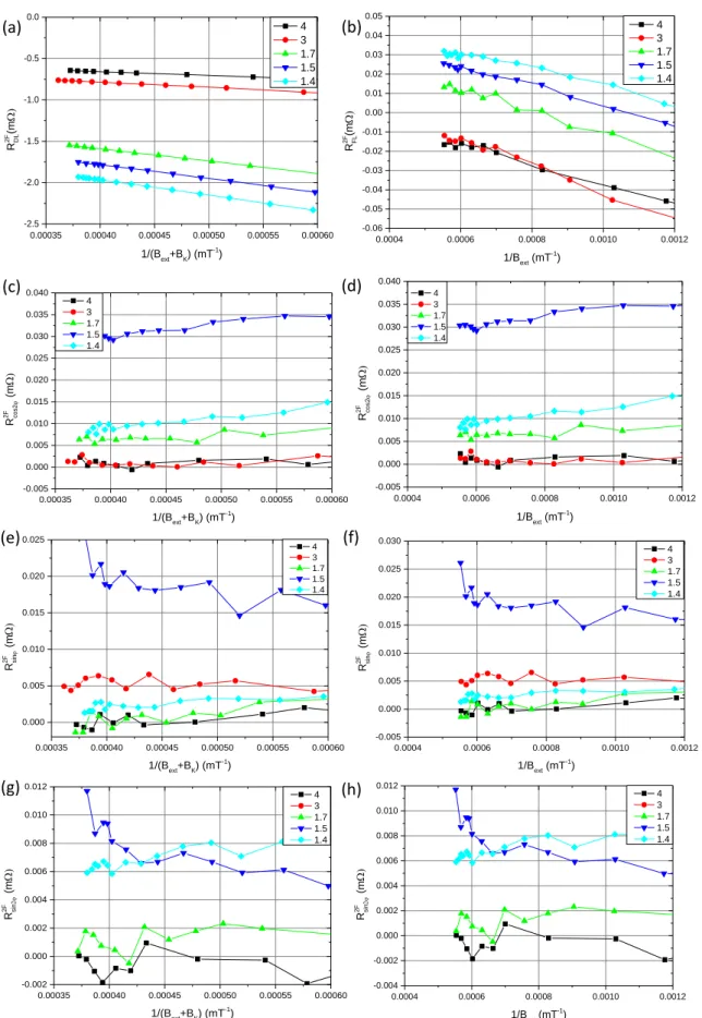
Ta3/Cu1/Co2/Pt1.5 (OX) (b) Ta3/Co2/W3. ... 25 Figure 3.12: (a) First and (b) second harmonic Hall resistance of Ta(3)/Pt(3)/Co(0.9)/MgO(0.9)/Ta(2). (c) The DL and thermal, and (c) the FL component extracted from the 2f resistance for different external field amplitudes... 26 Figure 3.13: Perpendicular field scan of the sample. The external field is swept perpendicular to the plane of the sample. ... 27 Figure 3.14: Out-of-plane angular scan. A constant field is rotated in a plane (shaded in light red) perpendicular to the sample plane. ... 27 Figure 3.15: Extraction of the perpendicular anisotropy field from the out of plane angle scan. (a) Dependence of the first harmonic resistance on the external field angle. (b) Anisotropy field as a function of the magnetization angle. (c) Anisotropy field as a function of the external field angle. BK0 and BK90 corresponds to the anisotropy when the magnetization is pointing perpendicular and in the plane of the sample. (d) Fit of the BK90 to be used to extract the SOTs. ... 28 Figure 3.16: Schematic depicting the progressive alignment of the perpendicular magnetization with the strength of the in-plane external field Bext. At lower fields, the magnetization can be staggered with a tilt along the perpendicular direction, corresponding to perpendicular magnetic domains, depicted by ML. At higher fields, MH, it is completely aligned with the external field... 29 Figure 3.17: Extraction of (a) the DL field and the thermal component and (b) the FL field from the corresponding 2F resistance, for an out-of-plane sample. ... 30 Figure 3.18: Comparison between keeping a constant BK and using the effective BK at each field. .... 30 Figure 3.19: Components of the second harmonic Hall resistance considering all the angular
symmetries. (a) DL and thermal (b) FL (c) cos2𝜑 (d) sin𝜑 (e) sin2𝜑 components. The black lines are the signals extracted from the measured second harmonic resistance and the red lines are the fits. 31 Figure 3.20: Amplitude of the 2F components against the external field. Dependence of (a) DL (c) cos2𝜑 (e) sin𝜑 (g) sin2𝜑 components on 1𝐵𝑒𝑥𝑡 + 𝐵𝐾 . Dependence of (b) FL (d) cos2𝜑 (f) sin𝜑 (h) sin2𝜑 components on 1𝐵𝑒𝑥𝑡. These denote the out-of-plane and in-plane effect of these 2f components on the magnetization. The numbers indicate the platinum thickness of the respective samples in nanometers of Ta(3)/Cu(1)/Co(2)/Pt. ... 32 Figure 3.21: Configurations of MOKE. (a) Polar (b) Longitudinal (c) Transverse. Ki and Kr denotes the incident and the reflected beams of light. While Ei and Er their polarizations. M denotes the
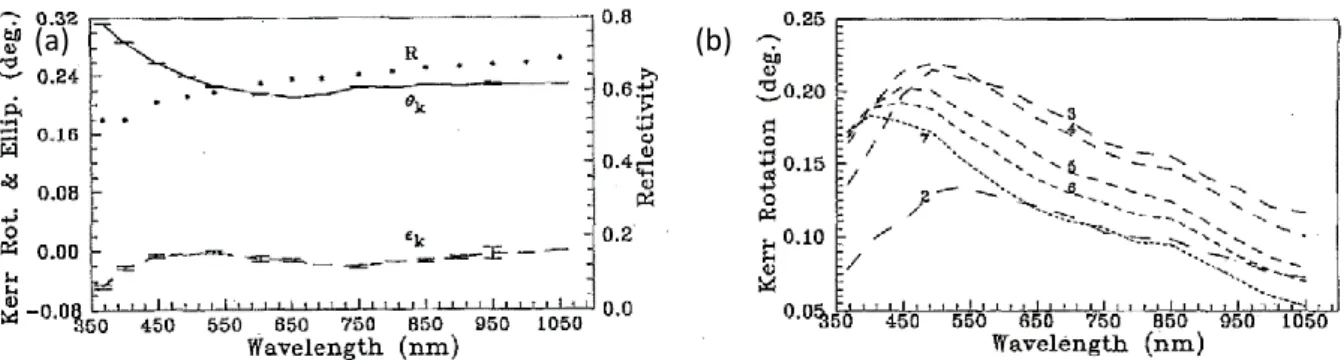
magnetization, depicted by the green arrow, and the cross product of m and E is depicted by the yellow arrow. The light blue plane denotes the plane of incidence. ... 34 Figure 3.22: Optical components of an in-plane MOKE. ... 36 Figure 3.23: Wavelength dependence of Kerr rotation 𝜃𝐾 of (a) Co/Pt and (b) Co/Pd superlattices. Figures adapted from ref 176 ... 37 Figure 3.24: Electrical setup used to inject sub-nanosecond current pulses into the sample. ... 37 Figure 3.25: Photograph of the in-plane MOKE set up along with the electrical components. ... 38
xiii
Figure 3.26: Examples of MOKE studies on in-plane magnetized samples. (a) Hysteresis loop (b) field switching (d) current induced domain wall motion in Ta (3)/Cu(1)/Co60Fe20B20(2)/Pt(2). (c) Current
induced switching of Ta (3)/Cu(1)/Co(2)/Pt(2). ... 39
Figure 3.27: (a) On-axis deposition and (b) Off-axis deposition. ... 40
Figure 3.28: Wafer level resistance maps of (a) on-axis and (b) off-axis deposited Pt 4.5 nm wafers. (c) and (d) resistance plots along the x=0 line of these maps. ... 41
Figure 3.29: Dependence of Pt thickness on conductance, based on calibration strips. ... 42
Figure 3.30: (a) Conductance of Pt calibration samples with respect to position on wafer. (b) Dependence of conductance on the thickness of platinum determined via optimization method. .... 42
Figure 3.31: (a),(b) Saturation magnetization, (c), (d) extraction of dead layer thickness and average Ms and (e), (f) extraction of interfacial and volume anisotropies of Co(x)/Al(2) and Ta(3)/Cu(2)/Co(x)/Pt(3) respectively. ... 44
Figure 3.32: (a) Wafer level gds design. (b) Chip level gds design. ... 45
Figure 3.33: Single resist microlithography process flow. ... 46
Figure 3.34: Residual resist on a device with a capping layer of alumina. ... 46
Figure 3.35: Dual resist microlithography process flow. ... 48
Figure 3.36: Optical micrographs of (a) Hall cross device and (b) domain wall bus. (c) SEM image of Hall cross. ... 48
Figure 4.1: Schematics of (a) STT-MRAM and (B) SOT-MRAM indicating the switching CMOS transistor. Images obtained from SPINTEC. (c) TEM cross section of an MTJ integrated in a CMOS chip showing the different metallization levels. Image adapted from177. (d) Schematics of a CMOS integrated MTJ, adpated from ref.178. ... 51
Figure 4.2: Wave function character at the Γ point of optimally oxidized Fe/MgO interface. The different columns correspond to the Fe 3d and the O 2p orbitals. The three sub-columns correspond to the perpendicular (left) and in-plane (right) orientation of magnetization and the case with no SOI (center). Adapted from Yang et. al.88. ... 52
Figure 4.3: (a) Spin Hall angle versus atomic concentration of oxygen in WOx in a stack of SiOx(25)/WOx(6)/CoFeB(6)/TaN(2). Plot adapted from reference 108. (b) Efficiencies of DL and FL torques versus the oxygen flow in the chamber during deposition of PtOx in a stack of PtOx/NiFe/SiO2. Plot adapted from reference 109. ... 55
Figure 4.4: Experimental design. By varying the depth of oxidation in platinum layer, we can study and differentiate the interfacial and bulk mechanisms of SOT generation. ... 56
Figure 4.5: Dicing schematic of the wafer. The design is laterally symmetric. The platinum wedge is shown on the left. The color codes correspond to their respective functions in the experiments. Resistance and magnetic measurements are performed on the blue and green strips. The devices are fabricated on the orange colored strips. ... 57
Figure 4.6: The device stack used in this experiment: Ta(3)/Cu(1)/Co(2)/Pt(4-1). The light blue shading indicates the oxidized region, denoted as MOx. ... 57
xiv
Figure 4.8: Effect of oxidation on (a) conductance and (b) saturation magnetization. UO1 and OX1 refer to Un-Oxidized and Oxidized samples. L and R refer to the lateral side on the wafer. ... 59 Figure 4.9: Schematic of an ICP-RIE used for oxidation of our samples. Figure adapted from
reference179. ... 60 Figure 4.10: Effect of oxidation on (a) conductance and (b) saturation magnetization of two sets of samples. UO2 and OX2 refer to the second sample set. ... 61 Figure 4.11: XPS spectra of bulk Pt (a, c, e) and bulk Co (b, d, f) of OX1(1.97, 1.62, 1.5) samples
respectively. ... 62 Figure 4.12: Emission angle dependence of Pt (a, c, e) and Co (b, d, f) ions of OX1(1.97, 1.62, 1.5) samples. ... 63 Figure 4.13: Damping Like effective field normalized to (a) the total current and (b) the voltage across the device. It is also normalized to the width of the device (wPt) to account for any variation from the lithographic process. ... 65 Figure 4.14: Magnetic field H dependence of the ferromagnetic resonance spectra for a CoFeB based stack at different field angles 𝜃𝐻 . Plot adapted from ref. 123. ... 67 Figure 4.15: The external field angle 𝜃𝐻 dependence of (a) the resonant field HR and (b) the linewidth ΔH of the first set of samples UO1 and OX1. The numbers in the parenthesis indicate the thickness of the top Pt layer in nm. ... 68 Figure 4.16: The dependence of (a) the demagnetization field, (b) the first K1 and second K2 order anisotropies, (c) the saturation magnetization and (d) the g-factor on the thickness of the top
platinum layer. Here UO1, OX1, and UO2, OX2 refer to the first and second set of samples. REF refers to a reference sample without the top platinum layer, Ta(3)/Cu(1)/Co(2)/Al(2). ... 68 Figure 4.17: Schematic of an FMR dispersion spectra depicting the scattering process from the FMR mode to another mode of finite wave vector. Figure adapted from ref.124. ... 69 Figure 4.18: Dependence of the damping constant 𝛼 on the top platinum thickness. Here UO1, OX1 and UO2, OX2 refer to the first and second set of samples. REF refers to a reference sample without the top platinum layer, Ta(3)/Cu(1)/Co(2)/Al(2). ... 70 Figure 4.19: Spin-mixing conductance 𝑔𝑒𝑓𝑓 ↑↓ of the samples. ... 71 Figure 4.20: (a) The magnetic moment and (b) the damping constant α as a function of the oxygen concentration at the Co/Pt interface. Calculated using KKR-GF multiple scattering theory. ... 72 Figure 4.21: In-plane effective anisotropy field of the oxidized and un-oxidized samples. ... 73 Figure 4.22: Schematic of the free layer of (a) STT-MRAM, (b) MRAM with MgO and (c) SOT-MRAM with Co/Pt interfacial oxidation. ... 73 Figure 4.23: (a) Dependence of the conductance of the UO1 and OX1 samples on the Pt thickness. (b) The conductance of the strips perpendicular to the platinum gradient, of UO1. Plotted with respect to the transverse position on the wafer... 74 Figure 4.24: Conductance of (a) UO1 and (b) OX1 corrected for the curvature induced by the
deposition of all the layers. ... 75 Figure 4.25: (a) Dependence of the total conductance on the Pt thickness of the UO1. The red curve shows the FS fit to this data. Dependence of (b) resistance (c) conductance and (d) resistivity on the platinum thickness. The red curve in the last plot is a polynomial fit to the data. ... 76
xv
Figure 4.26: Schematic of the sample stack depicting the uniform plasma oxidation of the platinum
layer in light blue color. This layer is denoted as MOx in the figure. ... 77
Figure 4.27: Conductance of UO1 and OX1 plotted against (a) the platinum thickness and (b) the effective platinum thickness. The platinum oxide thickness is determined from the constant offset between the two curves of (a) at higher thicknesses of platinum. The corrected curves refer to the layer curvature correction. ... 77
Figure 4.28: Conductance of UO2 and OX2 plotted against (a) the platinum thickness and (b) the effective platinum thickness. ... 78
Figure 4.29: (a) Resistance and (b) resistivity as a function of Pt thickness of sample UO2. ... 78
Figure 4.30: Energy of the system as the oxygen atom is moved from the surface (right) of the Pt/Co/Pt towards the Co/Pt interface. ... 80
Figure 4.31: (a) Pt(3 ML)/Co(3 ML)/Pt(5 ML) structure used for the ab-initio DFT calculations. The grey circles denote Pt atoms and the blue Co atoms. (b) The structure with the oxygen atoms present at the Co/Pt interface denoted by the red circles. ... 80
Figure 4.32: Atomic magnetic moment of each plane of the system with and without the presence of the oxygen atom at the interface. ... 81
Figure 4.33: (a) Oxidation model with a uniform oxidation of Pt. (b) Oxidation model with pumping of oxygen into Co near the Co/Pt interface. ... 82
Figure 4.34: Conductance of the OX1 sample showing the Fuchs-Sondheimer fit. ... 83
Figure 4.35: (a) Resistance and (b) resistivity of the OX1 sample as a function of Pt thickness. ... 83
Figure 4.36: (a) Resistance and (b) resistivity of the OX2 sample as a function of Pt thickness. ... 84
Figure 4.37: (a) External field dependence of the spin-wave frequency of UO1(2.68). (b) The effective magnetization of UO1 and OX1 samples determined from BLS measurements. ... 86
Figure 4.38: BLS spectra of (a) UO1(2.68) and (b) OX1(2.39) measured at wave vector k = 18.09 rad/µm with an external field of 0.1T. The lorentzian fit is shown by the red line. The frequency difference between the counter-propagating waves are marked as Δf. ... 86
Figure 4.39: The wave vector dependence of (a) the frequency difference of the counter-propagating spin waves and (b) the frequency of the spin waves of the UO1(2.68) sample. The red line is the fit with the dispersion equation including the DMI and the yellow without. ... 88
Figure 4.40: (a) The volume-averaged DMI and (b) the interfacial DMI as a function of Pt thickness of UO1 and OX1 samples. The error bars include the errors in MS and Δf... 88
Figure 4.41: Exchange constant A as a function of (a) the Pt thickness and (b) the interfacial DMI. ... 88
Figure 4.42: Temperature dependence of (a) the magnetic moment and (b) the moment normalized at 150 K. ... 90
Figure 4.43: DL field normalized by areal magnetization and (a) current and (b) voltage across the sample. ... 91
Figure 4.44: DL fields normalized by (a) current and (b) voltage across the sample. The x-axis denotes the effective thickness of metallic Pt that contributes to the generation of the SOTs. ... 91 Figure 4.45: DL fields normalized by the areal magnetization and (a) the current and (b) the voltage across the sample. The x-axis denotes the effective metallic Pt contributing the generation of SOTs.92
xvi
Figure 4.46: Damping like SOT efficiency per unit applied (a) current density in Pt and (b) the electric field across the device, as a function of effective Pt thickness. ... 93 Figure 4.47: (a) DL field normalized by the current density in the HM for various systems. Plot
adapted from data already published in a previous thesis174. (b) DL SOT efficiency normalized by the current density, fit with the Pt conductivity denoted by the red curve. ... 94 Figure 4.48: Effective Pt thickness dependence of the FL field normalized by the magnetization and (a) the current and (b) the voltage across the device. ... 95 Figure 4.49: Dependence of FL SOT efficiencies on effective Pt thickness, normalized by (a) current density through Pt and (b) electric field across the Hall cross. Values determined using the linear fit method. ... 95 Figure 4.50: Comparison of the DL and FL fields, normalized by (a) the current density in Pt and (b) the electric field across the Hall cross. ... 96 Figure A.1: Dependence of the amplitude of the FL component of the 2nd harmonic resistance normalized by the PHE coefficient on the inverse of the external field for (a),(c),(e) un-oxidized and (b),(d),(f) oxidized samples. ... 98 Figure A.2: Dependence of the FL field normalized by (a) the current and (b) the voltage across the device, on the Pt thickness. The data-points with the crosses denote the values extracted from the polynomial fit. ... 99 Figure A.3: Effect of the strength of the external field on the magnetization of the Co film. At
moderate fields, the magnetization denoted by ML lies in the plane of the film while at higher fields, the magnetization denoted by MH lies along the external field direction. ... 100 Figure B.1: Variation of (a) the Conductance and (b) the magnetic moment of the oxidized and
unoxidized Co sample along the Co wedge. Here the strip number refers to the number of the strip along the wedge with 1 being the thickest part and 28 being the thinnest………. 101 Figure B.2: (a) Field-scan of CoOX sample indicating the presence of higher-order anisotropies. (b) Variation of the DL field along the Co wedge, normalized by the applied current………. 102
xix
Acknowledgements
The work presented here has been possible due to the encouragement, guidance, help, and support of many.
First and foremost, I would like to thank my thesis supervisors, Gilles Gaudin and Mihai Miron. Not only did they advise me on scientific matters, but they have become good friends during this work. The characteristics that have had a lasting impression on me are Mihai’s intellectual curiosity and ability to break down complex scientific phenomena into simple, bite-sized pieces; And Gilles’ humility and soft spoken-ness, diligence and his vast repertoire of knowledge. I can only aim to inculcate these standards that they have set for me, in my professional and personal life. Thank you both for standing by me during the good times and bad.
As probably is the case for many theses, I experienced difficulties, setbacks and hidden pitfalls during my thesis. From dicing induced sample damage to indium contamination from the sputtering target; and platinum oxidation from the residue of standard nitrile gloves. However, contrary to what I think of others, these pitfalls did not disappear on the day of the defense, which took place on the first day of French strikes, Dec. 5th, 2019. I would like to thank all the thesis committee members who managed to make it regardless of the travel difficulties. Mairbek Chshiev, Felix Casanova, Michel Viret and Mihai Gabor. Their valuable insights and their critical review of my work are greatly appreciated.
I would also like to thank my collaborators around the world. Ali Hallal and Mairbek Chshiev for the ab-initio calculations; Mihai Gabor for the FMR measurements; Sebastien Labau, Aymen Mahjoub and Bernard Pelissier for the AR-XPS measurements; Avinash Kumar Chaurasiya, Amrit Kumar Mondal and Anjan Barman for the BLS measurements; Eric Gautier for the TEM measurements; Peter Mills and Thomas Saerbeck for the neutron reflectometry measurements.
My special thanks to the people from SPINTEC who made significant contributions to this work. Alexandru Trifu, with whom I started this work on platinum oxidation; Stéphane Auffret for the countless sample depositions and Isabelle Joumard for the technical support.
I have further obtained help and guidance from the members of the SOT group at SPINTEC. Thomas Brächer for his help with fabrication and guidance; Mohamed Ali Nsibi, with whom I started this Ph.D. program and built a couple of MOKE microscopes with; Haozhe Yang from whom I learned the importance of putting together a quick setup to test something quickly; Alexandre Mouillon and Marc Drouard for help with the measurement setup and data analysis; Eva Schmoranzerova for being a sounding board for SOT measurements; Pyunghwa Jang, Edmond Chan, and Ugwumsinachi Oji for help with measurements; Mathieu Fabre for introducing me to Python; Soong-Geun Je for helping with the electrical setups.
I would also like to thank the members of the PTA for their valuable help in the fabrication of my devices, namely, Thierry Chevolleau, Jean-Luc Thomassin, Frédéric Gustavo, Marlène Terrier, Christophe Lemonias, Thomas Charvolin, Nicolas Chaix, Irène Peck, Guillaume Lavaitte, Jude Guelfucci, and Nathalie Marini.
My sincere gratitude to all the members of SPINTEC, past, and present. I have gained valuable guidance, insight and technical advice from many of you. Bernard Dieny, Ursula Ebels, Lucian Prejbeanu, Mairbek Chshiev, Vincent Baltz, Laurent Vila, Olivier Boulle, Claire Baraduc, and Olivier Klein; Lucian Prejbeanu and Olivier Fruchart for maintaining the welcoming atmosphere at SPINTEC for
xx
PhDs and post-docs; Catherine Broisin, Rachel Mauduit, Sabrina Megias, Léa Althana and Céline Conche for help with all the administrative work; Daniel Solis Lerma for taking time to answer all my theoretical questions; Paulo Coelho and Jyotirmoy Chatterjee for help with the VSM; Léa Cuchet and Clarisse Ducruet (affiliated with Crocus Technology) for the same; Eric Billiet for the technical support; Roméo Juge, Titiksha Srivastava and Marco Mansueto for helping set up the pot de thèse; My officemates Cécile Naud and Caroline Thibault. In addition, I would like to thank all the members of SPINTEC for the numerous discussions over coffee or otherwise and helping make these years memorable.
My gratitude to the Université Grenoble Alps, SPINTEC, IRIG, CEA and CNRS for accepting me as a doctoral student. And to the European Union for funding my doctoral program under the Horizon 2020 program (Project 638656 Smart Design). I would also like to thank the École Doctorale de Physique for accepting the extension of my thesis, allowing me to wrap up my work completely.
There are people whose advice and guidance I have sought over the years and which has been highly valuable in this journey. A special thanks to all my mentors for taking time out of your busy lives to guide me.
I would finally like to thank my friends and family. There’s more to life than the work presented here. From climbing mountains to having a nice soirée to just keeping me grounded. You all add color to my life. Thank you!
1
Chapter 1 Introduction
A diversified demand stemming primarily from consumer products and Internet of Things (IoT) devices has led to a spurt in the growth of the memory industry in the past decade. This has also led to faster adoption of Non-Volatile Memory (NVM) technologies such as Magnetic Random-Access Memories (MRAM). MRAMs are high-speed, low-power and non-volatile spintronic memories. It uses the Tunneling Magneto-Resistance (TMR) mechanism for the readout of the memory bit and can use either the Spin-Transfer Torque (STT) or the Spin-Orbit Torque (SOT) mechanism for the write operation. The schematics of STT-MRAM and SOT-MRAM are as shown in Figure 1.1.
Figure 1.1: Schematics of (a) STT-MRAM and (b) SOT-MRAM
In SOT-MRAM, the write current is injected in the plane of the magnetic bit, decoupling the read and write paths. This leads to a lower current flowing through the oxide tunnel barrier, slowing the oxide aging and enhancing the overall endurance of the bit. Furthermore, this also enables the use of a tunnel barrier with a higher Resistance-Area (RA) product, leading to a lower read disturb and hence increased reliability. SOT-MRAMs typically use a tri-layer structure with inversion asymmetry. A current injected into the heavy metal (HM) layer with high Spin-Orbit Coupling (SOC) gives rise to various torques, namely the Field-Like (FL) torque and the Damping-Like (DL) torque. These torques act on the magnetization of the adjacent Ferro-Magnetic (FM) layer in order to switch it during the write
Introduction
2
operation1,2. They originate primarily from two distinct mechanisms – the Spin Hall Effect (SHE), which is a bulk effect and the Inverse Spin Galvanic Effect (ISGE), which is an interfacial effect. The efficiency of these torques determines the write energy. It also determines the size of the switching transistor and correspondingly the overall memory density. Hence, it is vital to determine the mechanism underlying the SOTs in order to be able to engineer it for industrial applications.
Chapter 2 delves into the physics underlying these mechanisms. Starting from a short introduction to
the geometric Berry phase, the reader is introduced to concepts such as the Spin-Orbit Interaction (SOI), the various Hall effects, the Rashba effect, and the spin-orbit torques. A clear understanding of these concepts is needed to appreciate the core of this work.
Chapter 3 details the tools utilized to complete this study. Importantly, it details the 2nd harmonic torque measurements, which is a powerful technique to not just to quantify the torques, but also gain insight into the magnetic system itself. This chapter also describes the successful construction and test of a Magneto-Optical Kerr Effect (MOKE) microscope capable of imaging ultra-thin magnetic structures which are magnetized in the plane of the film. It closes detailing the sample deposition, characterization and fabrication processes. This chapter is not exhaustive in its coverage of the numerous experimental techniques used in this study. However, these are described as and when encountered in the narrative of this work.
A large emphasis is placed on the energy efficiency of these MRAMs to be better positioned alongside their CMOS counterparts. Various approaches have been studied ranging from clever device designs to even cleverer utilization of the underlying physics to one’s advantage. One such method that has witnessed significant research interest recently is the oxidation of the system. Oxidation has been the subject of intense scrutiny in both the academia and the industry since its utility in manufacturing Magnetic Tunnel Junctions (MTJ) with a perpendicular orientation of the magnetization was established. Hence, it is only natural that this knowledgebase is extended to SOTs. Different groups have studied the effect of oxidation of the Ferro-Magnetic (FM) layer and more recently the heavy metal layer on SOTs. HM oxidation has been described to generate SOTs comparable in strengths to that of Topological-Insulators (TI). Such an enhancement of torques could lead to a lower write current, and thereby higher energy efficiency and bit density of SOT-MRAMs. This increase in DL torques should also correspond to an increase in PMA, which determines the thermal stability of pMTJs. Hence, the oxidation of the HM appears to be a vital tool in the development of SOT-MRAMs for longer retention times and a net reduction in write energy.
Chapter 4 studies the mechanism of SOTs in platinum oxide systems. Beginning from a description of
our devices on a 4” wafer, which enables us to make comparisons on a uniquely deposited sample, the premier section details extensive material characterizations which help gain knowledge into the material system and the oxidation process. This is followed up by experimental techniques which enable us to quantify the SOTs in these systems. We then rely on experimental and modeling techniques to build a model of the oxidized system, which is then pursued to understand the mechanism behind the observations.
Such detailed studies are a pre-requisite for any new technique to mature out of the laboratories. Extensive experimental and modeling works along with sound arguments are presented to the reader in support of the conclusions of this work.
3
Chapter 2 Background
In order to engineer our SOT devices, it is necessary to understand the relevant mechanisms that are present in such systems. This chapter discusses the phenomena underlying SOTs. We start out by describing the geometrical phase which can give rise to various transverse transport phenomena. We then consider this Hall type transport/ spin accumulation in the context of our system and the torques it can generate. A clear understanding of these mechanisms is needed to engineer SOT devices towards certain metrics such as energy efficiency, longer data retention time, etc. This chapter provides a brief introduction to these mechanisms.
2.1 Geometric Phase in Solids: Pancharatnam-Berry Phase
A quantum mechanical system, transported adiabatically around a closed loop in the external parameter space (magnetic field, electric field, etc.) acquires a dynamical phase, which depends on the energy of the system and the time it takes for the system to complete the loop, and a geometric phase which depends only on the geometry or the topology of the loop3–5. This geometric phase is known as the Pancharatnam-Berry phase or the Berry phase, which was discovered by S. Pancharatnam during his work on the interference of polarized light in 19566 and generalized by M. Berry in 19843.
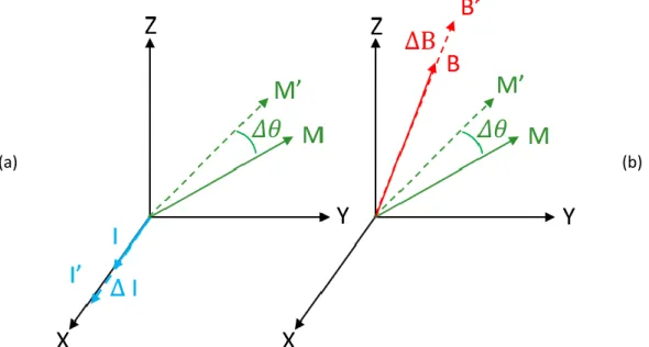
Consider a vector that is always tangential to the surface. In the case of a flat surface, shown in Figure 2.1a, any translation of the vector in a closed loop (A’-P’-B’-Q’-A’) without rotating the vector around the surface normal, returns the vector to its original state. In the case of a curved surface, shown inFigure 2.1b, this is no longer the outcome. A translation around a closed loop will result in an accumulated angle which is solely dependent on the geometry of the path. This accumulated angle, θ, is known as the anholonomy angle or the Hannay angle in mechanics.
In the case of a quantum mechanical system described by a Hamiltonian H(R) that depends on a set of external parameters R(t) = (R1, R2…), the Schrödinger’s equation can be written as 4,5:
𝐻(𝐑)|n
⟩
= 𝐸𝑛(𝑹)|n(𝐑)⟩
(2.1)
with eigenvalues 𝐸𝑛(𝑹) and eigenvectors |n(𝐑)
⟩
. By performing an adiabatic closed-circuit 𝐶 in theparameter space, the system acquires a phase given by
Spin-Orbit Interaction
4
(a) (b)
Figure 2.1: Parallel transport (a) on a Euclidean plane and (b) on a cylinder. ϴ denotes the anholonomy angle. Figure adapted from ref. 7.
Here |ψ(𝑇)
⟩
and |ψ(0)⟩
are the final and initial states, 𝛿𝑛 is the dynamical phase and 𝛾𝑛(𝐶) is thegeometric Berry phase. The berry phase can be re-expressed in terms of the Berry vector potential or the Berry connection as 4,5:
𝛾𝑛(𝐶) = ∮ 𝑨𝐶 𝑛(𝐑). 𝑑𝑹
(2.3)
Here 𝑨𝑛(𝐑) is gauge dependent whereas the berry phase 𝛾𝑛(𝐶) is a gauge-invariant, i.e. it is a physical
quantity that can only be changed by an integer multiple of 2π under gauge transformation. Further, the Berry phase depends only on the geometrical aspect of the closed path and not on the time variation of the external parameters.
Following Stokes theorem, the Berry phase can also be re-written in terms of Berry curvature Ω𝑛(𝐑)
as
𝛾𝑛(𝐶) = ∬ Ω𝑆 𝑛(𝐑)𝑑𝑅1𝑑𝑅2
(2.4)
The Berry curvature describes the local geometric properties of the parameter space. In the case of a two-level system, it can be shown that the Berry curvature acts as the magnetic field generated by a monopole at the origin and the Berry phase acquired along a circuit is the flux of the monopole through the surface subtended by the circuit, 𝐶. The vector potential of this magnetic field is the Berry connection, 𝑨𝑛(𝐑).
2.2 Spin-Orbit Interaction
A crystalline solid can be considered as a periodic lattice of ions, each generating its own local electric field E. Following the Lorentz transformation, an itinerant electron moving through such a crystal lattice will observe this local electric field as a magnetic field B ~ (v x E) in its frame of reference. Here
v is the velocity of the electron. Because of this local effective magnetic field, the spin of the electron
will try to align antiparallel to the effective field in order to minimize the energy. This, in turn, locks the spin of the electron to its momentum and is known as spin-momentum locking. The spin-orbit (SO) Hamiltonian is given by
𝐻𝑆𝑂=
𝑔𝑠µ𝐵
5
denoting the locking of the electron’s spin S and its momentum K. This Spin-Orbit Interaction (SOI) gives rise to various physical phenomena in magnetic materials, namely the magnetocrystalline anisotropy, magnetization damping, Anomalous Hall Effect (AHE), Anisotropic Magneto-Resistance (AMR), etc.
2.3 Berry phase in Hall Effects
As an electron moves through a crystalline solid, if the rate of change of the effective magnetic field is lower than that of the electron’s Larmor frequency, the electron spin can follow the field adiabatically, accumulating a Berry phase. In order to make the Berry phase a gauge invariant, physically observable quantity, it is necessary to have the path 𝐶 be closed. This can be achieved by applying an external magnetic field, inducing a cyclotron motion along a closed path in the momentum space, leading to magneto-oscillatory effects. The closed path can also be achieved by applying an electric field to vary the momentum across the entire Brillouin zone. In this case, the electron can acquire an anomalous velocity proportional to the Berry curvature. This anomalous velocity is transverse to the applied electric field, giving rise to the Hall effect. The Hall effect is the appearance of a voltage transverse to the applied current. This anomalous velocity manifests itself as a correction to the ordinary velocity which is given by the slope of the Bloch band, given by5:
𝒗𝑛(𝒌) =
𝜕𝜀𝑛(𝒌)
ℏ𝜕𝒌 −
𝑒
ℏ𝑬 × Ω𝑛(𝒌)
(2.6)
where the first term on the right accounts for the longitudinal velocity and the second term accounts for the transverse Hall velocity. Here, Ω𝑛(𝒌) is the Berry curvature of the nth band. The Berry curvature
is an intrinsic property of the band structure, is gauge invariant in itself and doesn’t require a closed-loop to be defined like the Berry phase. It is then necessary to determine under which conditions the Berry curvature plays a non-negligible role in the determination of the anomalous velocity. This can be done based on symmetry arguments. While 𝒗, 𝒌 and 𝑬 are antisymmetric with spatial inversion, only 𝒗 and 𝒌 change signs with time reversal. This results in the Berry curvature being odd with respect to time reversal and even with respect to spatial inversion symmetry. Hence, in crystals where both the time-reversal and the spatial inversion symmetry are broken, the effect of Berry curvature is negligible. However, in systems where only either one of the two is broken, the Berry curvature and in turn the transverse Hall velocity can be non-negligible.
The Hall effect is antisymmetric with respect to time reversal in the linear regime. Hence, a time reversal symmetry breaking term in the Hamiltonian is required to obtain a measurable Hall voltage. Although, there are 2D systems with time reversal symmetry, which exhibit non-linear Hall effect, these are beyond the scope of this work. Hence, centrosymmetric crystals with time-reversal symmetry,
𝐸(𝒌, 𝑠↑) = 𝐸(𝒌, 𝑠↓)
(2.7)
as plotted in Figure 2.2a, displays no Hall effect. It is necessary to have broken time-reversal symmetry, by the use of an external magnetic field or an exchange field. In case of latter, it is also necessary to have spin-orbit coupling in order to break the symmetry under a global rotation of π of the spins. There can also be systems with non-trivial texture of magnetization, which can give rise to Topological Hall Effect (THE) even in the absence of SOC. However, these too are beyond the scope of this work. The appearance of Hall voltage as a consequence of Berry curvature lies at the heart of various Hall effect type phenomena, namely the Anomalous Hall Effect and the Spin Hall Effect which are described
Anomalous Hall Effect
6
in the following sections. The contribution of the Berry curvature to these effects is considered an intrinsic part of the system.
2.4 Anomalous Hall Effect
The Anomalous Hall Effect (AHE) is the appearance of a voltage transverse to an applied current in Ferromagnetic (FM) metals. This can be attributed to intrinsic and extrinsic effects.
The intrinsic effect is related to the band structure of the metal and is as explained in the previous section. This contribution to the anomalous velocity was originally proposed by Karplus and Luttinger in 19548, who connected this phenomenon to the intrinsic SOI of the FM. However, it’s only recently that this has been connected to the topological Berry curvature of the Bloch bands. Consider the case of a system with SOI and an exchange field9. The Hamiltonian and the energy spectrum can be written as: 𝐻̂0= ℏ2𝑘2 2𝑚 + 𝜆(𝒌 × 𝝈̂) ∙ 𝒆𝑧− ∆𝝈̂𝑧 (
2.
8) 𝐸±(𝑝) = ℏ2𝑘2 2𝑚 ± √𝜆 2𝑝2+ ∆2 (2.
9)Here the first term of the Hamiltonian corresponds to the kinetic energy. This is shown in Figure 2.2a, which shows the energy spectrum in the absence of SOI and exchange fields The second term corresponds to the Spin-Orbit Coupling (SOC). This leads to a linear dispersion of the band structure giving rise to two energy bands with spin chirality (mixed spins). This is shown in Figure 2.2b, in the absence of a exchange field. Here the colors indicate the different energy levels 𝐸+(𝑝) and 𝐸−(𝑝) and
not the spin states. This Hamiltonian describes the Rashba effect, which is detailed in a later section. Here 𝜆 corresponds to the Rashba/SOC strength. The third term corresponds to the exchange field along the z-axis. In the absence of SOI, it leads to a splitting of the energy band as shown in Figure 2.2b. In the presence of SOI, this leads to a split gap in the energy spectrum given by 2∆ as shown in Figure 2.2d, also referred to as anti-crossing points in some cases. These figures were plotted with the parameters: m=1, 𝜆=4, ∆=2.
Here the exchange field breaks the time-reversal symmetry and the SOI connects the spin of the electron to its orbital trajectory. The SOI, along with the broken time-reversal symmetry induces a Berry curvature in the band structure. This Berry curvature can be written as5:
Ω±= ∓
𝜆2∆
2(𝜆2𝑘2+∆2)3/2 (2.10)
The Berry curvature of the two bands are concentrated in the energy gap at k = 0 and have opposite signs, as shown in Figure 2.3. This constitutes the intrinsic contribution to the AHE and its strength varies depending on the position of the Fermi level with respect to the energy gap. Figure 2.3 was plotted with the parameters: m=1, 𝜆=4, ∆=4.
7
(a) (b)
(c) (d)
Figure 2.2: Energy dispersion curves in the presence of (a) no SOI or exchange field (b) only exchange Field (c) only SOI (d) SOI and exchange fields. The vertical axis denotes the energy and the horizontal axis denotes the momentum. The colors indicate different energy bands.
Figure 2.3: The Berry curvature of the two energy bands. It is opposite in signs and has a maximum at the energy gap. Here the vertical axis denotes the Berry curvature and the horizontal axis the wavenumber. The colors represent different energy bands.
Rashba Effect
8
The AHE can also have extrinsic contributions from scattering events, namely, skew scattering and side jump10. Skew scattering refers to the asymmetric scattering of the electron due to impurities, depending on SOI. This can be visualized in terms of the scattering cross-section, which depends on the spin state of the electron. The scattering angle of the electron depends on the relative orientation of its spin with respect to the effective magnetic field of the impurity that it experiences. This results in the asymmetric scattering of the electron depending on its spin state, leading to a transversal spin current. Skew scattering dominates in the low temperature, clean sample limit. However, at room temperature, in dirty samples, it is expected to play a smaller role. This can be worked out by adding an impurity related term to the Hamiltonian given in eq. 2.89.
Side jump is a purely quantum mechanical effect that refers to the spin-dependent displacement of the electron at impurity sites. Consider an itinerant electron traveling with a wavevector k. Scattering with an impurity with SOI will lead to a displacement transverse to k. However, the initial and final direction of motion remains the same. Upon comparison with the intrinsic mechanism, the intrinsic band structure related effect is expected to be the dominant one in transition metal ferromagnets11 and should be so in our case as well.
2.5 Rashba Effect
In crystals with broken inversion symmetry, an internal electric field can be present which can give rise to SOI. This is true in the case of non-centrosymmetric zinc-blende structures as shown by Dresselhaus12 and in systems with broken structural inversion symmetry as shown by Vas’ko13 and Bychkov and Rashba14. The SO Hamiltonian in this case can be written in terms of the electron momentum as15
𝐻𝑆𝑂(𝒑) = −µ𝐵(∇𝑉 × 𝒑 ). 𝝈/𝑚𝑐2 (2.11)
In this case, the SO Hamiltonian must be odd in momentum to preserve the time-reversal symmetry (𝐻𝑆𝑂(−𝒑) = −𝐻𝑆𝑂(𝒑)). This is valid only in systems with broken spatial inversion symmetry. In
systems studied in the work, the inversion symmetry is broken in the vertical z-direction giving rise to an interfacial electric field of the form 𝑬 = 𝐸𝑍𝒆𝑧. This results in a SO Hamiltonian of the form
𝐻̂𝑅= 𝛼𝑅(𝒌 × 𝝈̂) ∙ 𝒆𝑧 (2.12)
Here is the 𝛼𝑅 Rashba parameter which denotes the strength of this coupling and is the 𝝈̂ Pauli spin
matrices. This has the same form of the Hamiltonian shown in eq. 2.8. This leads to spin-momentum locking and spin-split sub-bands as mentioned in the earlier section. Hence, when electrons pass through such a system, they experience the effect of the internal electric field in the form of an effective magnetic field, the Rashba field 𝐵𝑅. This causes the spins to precess around the direction of
the Rashba field. This is shown in Figure 2.4. In case of paramagnetic materials, this leads to the polarization of the electrons along the direction of the field and is known as the inverse spin galvanic effect (ISGE) or the Edelstein effect from his seminal work on this topic16.
9
When a thin magnetic film is deposited on top of such a system, this polarization or accumulation of electron spin can exert a torque on the magnetization as was first demonstrated by Miron et al.17. This mechanism is detailed in a later section. It is to be noted that due to the screening effect in metals, this Rashba field is present only at the interface, on the order of a few Å. Further, it can also be described in terms of Berry curvature given by15
𝛀(𝒑) ∝ 𝛼𝑅∇𝑝× (𝝈̂ × 𝒑) (2.13)
This can be considered as the curl of the spins orthogonal to the momentum. Hence, it can also give rise to a current in the transverse direction when the time-reversal symmetry is broken.
2.6 Spin Hall Effect
The Spin Hall Effect (SHE) is the phenomena analogous to AHE, seen in normal metals (NM). Upon injecting a current into an NM with a large SOC, a transverse pure spin current is produced with a polarization perpendicular to the plane of the charge and spin current. Unlike the AHE, where the FM leads to a difference in majority and minority carries giving rise to a detectable transverse voltage, in SHE such detectable signals are lacking. Hence the early experiments used optical detection techniques18,19. Soon this technique was used to switch adjacent magnetic layer via Spin Transfer Torque (STT)1,2.
The source of SHE is almost exactly the same as that of AHE and can be divided into intrinsic band structure based contributions and extrinsic impurity based ones. In case of the intrinsic contribution, the mechanism can be described by including a term describing the SOC. The initial theoretical works used either a Luttinger Hamiltonian which describes interacting electrons in semiconducting systems20 or a Rashba model as described in the previous sections21. However, care must be taken to avoid over-simplification of the band structure, which could lead to the cancellation of the calculated intrinsic contribution by the extrinsic contributions22. This Hamiltonian can also be obtained from ab-initio calculations and then using a Kubo formalism, which describes the linear response of a quantity due to a time-dependent perturbation, we can obtain the longitudinal and transverse spin and charge conductivities23. The Berry curvature can also be obtained this way23,24. These theoretical studies reveal that as in the case of AHE, the band structure of the material plays an important role in SHE.
The left panel of Figure 2.5a shows the band structure of platinum calculated this way23. Comparing it with the spin Hall conductivity (SHC), it is evident that the conductivity peaks when the SOC splits the doubly degenerate d bands at the L and X high symmetry points. The SHC can be varied depending on the position of the Fermi level. This is consistent with the calculated Berry curvature which has similar peaks at L and X points, as shown in Figure 2.5b.
Figure 2.4: An electron moving in a Rashba system experiences a transverse Rashba magnetic field which causes the spin to precess around this field. Figure adapted from Manchon et. al.15
Spin Hall Effect
10 (a)
The SHC of transition metals has been widely studied. It can either be positive or negative depending on the filling of the d shell. Metals with d shells more than half-filled such as Pt, Pd, Au have a positive SHC whereas the ones with less than half-filled d shells such as Ta, Nb, W, Mo have negative values24, indicating a dominant band structure-dependent intrinsic contribution to SHE.
The SHE can also have extrinsic contributions due to impurities, namely skew-scattering and side-jump mechanisms. Just as in AHE, the skew-scattering contribution is proportional to its transport lifetime τ. It arises from the asymmetric contribution to the disorder scattering in metals with SOC. The side-jump mechanism, on the other hand, is independent of the transport lifetime and arises from the transverse displacement of the electron upon scattering with an impurity. These mechanisms are analogous to the ones detailed for AHE.
The SHE leads to the generation of a transverse pure spin current upon the injection of a charge current. This is quantified in terms of the Spin Hall Angle (SHA) 𝜃𝑆𝐻𝐸 which is given as the ratio between
the SHC, 𝜎𝑆𝐻𝐸, and the longitudinal conductivity, 𝜎𝑥𝑥 :
𝜃𝑆𝐻𝐸 =
𝜎𝑆𝐻𝐸
𝜎𝑥𝑥 (2.14)
This defines the efficiency of the material to generate spin currents upon the injection of a charge current. Another parameter of interest here is the spin diffusion length 𝜆𝑁𝑀 which denotes the average
distance the spins travel before they flip. Non-magnetic transition metals can have a spin diffusion length of the order of a few nm.
(b)
Figure 2.5: (a) Left panel: band structure, and right panel: spin Hall conductivity (SHC) of platinum fcc structure. (b) The corresponding Berry curvature at zero temperature. Plots adapted from Guo et. al.23.
11
2.7 Spin-Orbit Torques
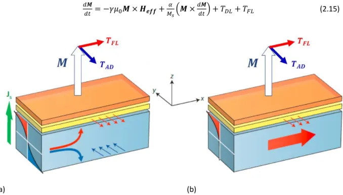
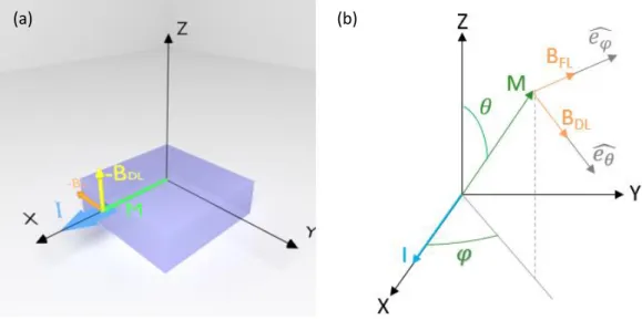
The SOT device element that we are concerned with consists of FM/NM bilayer system. Injection of an in-plane current, through the SOC mechanism (SHE and Rashba), generates torques that act on the magnetization of the FM layer, which is the magnetic memory element. This causes it to switch its orientation of magnetization. This is the basis of SOT-MRAM. The need for such a bi-layer system to generate torques are twofold: the SHE in the HM results in a pure spin current which can flow into the FM layer causing it to switch and the broken spatial inversion symmetry results in Rashba effect at the interface causing spin accumulation at the interface which can then act on the FM layer. Figure 2.6a shows the effect of SHE in a bi-layer system. Here the SOC leads to a spin current perpendicular to the device plane. These spins, initially polarized along an axis dictated by the SHE, precesses around the magnetization axis and dephases. In doing so, it transfers its angular momentum to the magnetic moment of the FM layer according to the conservation of angular momentum. This is the Spin Transfer Torque (STT) mechanism. Figure 2.6b shows the Rashba effect which is present in metals with a large SOC and broken inversion symmetry. In this case, there is a spin accumulation/reorientation along the FM/NM interface. These spins can act on the magnetization of the FM layer via the exchange mechanism.
As in the case of STTs, the SOT acting on the magnetic element can be split into two orthogonal torques, namely the Anti-Damping Torques (ADT), also known as the Damping - Like Torques (DLT), and the Field-Like Torques (FLT) as shown in Figure 2.6and Figure 2.7. They are named so because they are analogous to the torques acting on a magnetic moment in a magnetic field (for a particular direction of magnetization). The direction of the AD field depends on the orientation of the magnetization, similar to the Gilbert damping, whereas the direction of the FL field is fixed by the polarization of the spin accumulation and in turn orients the magnetization along that direction, equivalent to the effect of a Zeeman field. These torques can be modeled as two additional terms in the Landau- Lifshitz equation (LLG) given by 𝑑𝑴 𝑑𝑡 = −𝛾𝜇0𝑴 × 𝑯𝒆𝒇𝒇+ 𝛼 𝑀𝑠(𝑴 × 𝑑𝑴 𝑑𝑡) + 𝑇𝐷𝐿+ 𝑇𝐹𝐿 (2.15) (a) (b)
Figure 2.6: SOT acting on the magnetization M of the FM as a result of (a) SHE (b) Rashba effect. Figure adapted from references 25,26.
Spin-Orbit Torques
12 Where,
𝑻𝑫𝑳= 𝑇𝐷𝐿(𝑴 × (𝑴 × (𝑱𝒆× 𝑛̂))) (2.16)
𝑻𝑭𝑳= 𝑇𝐹𝐿((𝑱𝒆× 𝑛̂) × 𝑴) (2.17)
Here 𝑇𝐷𝐿 and 𝑇𝐹𝐿 correspond to the strength of the damping-like and field-like torques respectively.
These torques lead to effective fields that act on the magnetization, given by
𝑩𝑫𝑳= 𝐵𝐷𝐿((𝑱𝒆× 𝑛̂) × 𝑴) (2.18)
𝑩𝑭𝑳= 𝐵𝐹𝐿(𝑴 × ((𝑱𝒆× 𝑛̂) × 𝑴)) (2.19)
Where 𝐵𝐷𝐿 and 𝐵𝐹𝐿 corresponds to the strength of the damping like and field like fields respectively.
It is to be noted that higher-order terms can also have a significant contribution to the torques as described in ref. 27. Also, the sign convention used here is based on that of a standard right-handed precession of a magnetic moment in the presence of an external magnetic field.
Interfacial scattering plays a significant role in such systems. Recent works considering a full 3D transport with electrons that can cross and scatter across the FM/NM interface with the applied field, show a significant interfacial contribution to DLT and FLT28,29. Recently there has also been works showing SOTs can be generated by the AHE in FM/NM/FM multilayers30 and by Planar Hall Effect (PHE) in NM/FM/NM multilayers31. It has also been predicted32 and experimentally demonstrated33 that a transverse spin current with a polarization misaligned with the magnetization can be generated in an FM, upon injecting a current. These works show that although more effort is needed to have a comprehensive picture of the SOT phenomena, it can lead to more novel and efficient spintronic devices.
Figure 2.7: The SOTs acting on the FM layer can be decomposed into two orthogonal torques which effectively act on the magnetization in the form of two effective fields, the Damping-Like (DL) and the Field-Like (FL).
13
Chapter 3 Experimental Methods
This chapter details the experimental methods used in this work. It primarily consists of second harmonic torque measurements, in-plane Magneto-Optical Kerr Microscopy (MOKE) and sample deposition and metrology. Other techniques such as Reactive Ion Etching (RIE), Angle-Resolved X-ray Photoelectron Spectroscopy (AR-XPS), Ferro-Magnetic Resonance (FMR), etc. are detailed in later chapters when needed. This chapter also describes the sample fabrication techniques used for this work.
3.1 Second Harmonic Torque Measurement Technique
The second harmonic torque measurement is a powerful technique to extract the SOTs of different material systems. The FM can have in-plane or out-of-plane anisotropies including higher-order terms. This harmonic technique is also versatile, being useful to determine system properties when coupled to polarized light, thermal gradient, etc. or other specific applications such as to determine the dry friction of a magnetic layer, which can be helpful for Magnetic Tunnel Junction (MTJ) based memristive applications34.
We quantify the SOTs of our samples using this measurement technique. This method consists of a standard Hall measurement setup wherein our samples are patterned into a Hall cross, as shown in. A small alternating current of 10 Hz is applied along one of the arms while the transverse voltage is measured along the other. Further, the magnetization can be rotated using an external field. This is a quasistatic measurement technique wherein the magnetization of the magnetic material is made to fluctuate in the small-angle regime using an AC current with a small frequency, 10Hz in our case. Its frequency is not high enough so as to activate the magnetization dynamics in the Gigahertz range. The working principle is as depicted in Figure 3.1. When a DC current is applied in our sample the magnetization of the sample is at a certain equilibrium position denoted by M in Figure 3.2 (a) dictated by the balance of the current-induced SOTs, the anisotropy including the demagnetizing field. This equilibrium position of the magnetization can also be attained using an external field B, as shown in Figure 3.2 (b). When a small change is induced in the applied current (using e.g. a small AC current as in our measurements), denoted by ΔI, the magnetization will fluctuate in the small-angle limit, denoted by ΔѲ. This will result in a new position of the magnetization denoted by M’. We can achieve this same position of magnetization by changing the externally applied field as well, denoted by B’. Hence by