HAL Id: hal-00578913
https://hal.archives-ouvertes.fr/hal-00578913
Submitted on 19 Apr 2021
Fabrication and characterization of acoustic waveguides
using Silicon/PPT/Silicon structures and analysis of
diffraction effects for various modelings
F. Bassignot, G. Ulliac, Thierry Laroche, J. Garcia, E. Courjon, S.
Ballandras, J.-M. Lesage
To cite this version:
F. Bassignot, G. Ulliac, Thierry Laroche, J. Garcia, E. Courjon, et al.. Fabrication and
characteri-zation of acoustic waveguides using Silicon/PPT/Silicon structures and analysis of diffraction effects
for various modelings. 2010 IEEE International Frequency Control Symposium, Jun 2010, New Port
Beach, United States. pp.137-141, �10.1109/FREQ.2010.5556358�. �hal-00578913�
Fabrication and characterization of acoustic
waveguides using Silicon/PPT/Silicon structures and
analysis of diffraction effects for various modelings
F. Bassignot, G. Ulliac, T. Laroche, J. Garcia,
E. Courjon, S. Ballandras
lnstitut FEMTO-ST
UMR 6174 CNRS-UFC-ENSMM-UTBM 26 che. de l'épitaphe, 25000 Besançon, France
florent.bassignot@femto-st.fr
J.M. Lesage
CELAR DGA Rennes, France
Abstract—In this paper, we present new results on the
development of a new acoustic waveguide concept using an. acoustic wave excited by a Periodically Poled Transducer (PPT) and guided by guiding layers. Periodically poled transducers have been investigated recently as an alternative to classical inter-digital transducers for the excitation and detection of guided acoustic waves. The fabrication of PPTs operating in the
range 50 – 500 MHz has been achieved on 3 and 4 inches 500 μm
thick lithium niobate (LiNbO3) and tantalate (LiTaO3) Z-cut
wafers. The compact structure proposed allows high frequency
operation with a simplified package based on Si/LiNbO3/Si
material combination. Dispersion properties have been studied for this structure in order to find operating points corresponding to a specific thickness/period ratio. Two main devices have been fabricated, a Si/500 µm thick PPT/Si structure in order to validate the concept and a Si/20 µm thick PPT/Si structure to excite only one acoustic wave in the purpose of diffracting this wave. The experimental responses of the tested devices are compared to the predicted harmonic admittances, showing a good agreement between both results. The temperature sensitivity of the excited wave of both structures are also been measured and predicted. Finally, we expose different structures with impedance mismatches generating scattering effects.
I. INTRODUCTION
New guiding principles are currently investigated to develop high frequency devices capable to answer the RF manufacturer demand for telecommunication components. Nowadays, these components are more and more based on acoustic devices. In fact, acoustic resonators are usually based on surface or bulk acoustic waves but they are sensitive to their environment and present some technological limits. Passive components using trapped acoustic waves are thus well-suited for such an application. We suggest a compact structure allowing to guide an acoustic wave operating at high frequency. An acoustic wave is excited by a Periodically Poled Transducer (PPT) which is an alternative to classical inter-digital transducers. This wave is then trapped within a guiding structure. LiNbO3 and LiTaO3, as two piezoelectric and
ferroelectric materials, are tested to fabricate successfully PPTs and silicon substrates are used to guide the acoustic wave and allow a low cost package. Many diffraction analyses are studied to define the best configuration enabling to reflect in-phase the acoustic wave generated in order to exhibit a resonance behavior.
We describe the fabrication process of the new acoustic waveguides. These devices result from the development of piezoelectric transducers based on periodically poled ferroelectric domains in a LiNbO3 and LiTaO3 thinned plate bonded between two silicon wafers. By the dispersion properties analysis, we obtain operating points corresponding to a specific thickness/period ratio. We present new experimental results of acoustic waveguides based on sandwich structures as Si/LiNbO3/Si material combinations. We report theoretical results using our finite and boundary element (FEM-BEM) simulation tool. We expose different structures with impedance mismatches generating scattering effects.
The dispersion properties analyses have shown an optimum thickness of the ferroelectric plate, corresponding to the maximum electromechanical coupling coefficient, is found for each PPT period. Si/PPT/Si test vehicles, exhibiting a 50 µm period and a 20 µm thick ferroelectric layer, have pointed out the existence of an isolated mode operating at frequencies near 110 MHz for a LiNbO3 PPT. Moreover, we have demonstrated experimentally and theoretically that the temperature coefficient of frequency of thinned LiNbO3 is smaller than the one of thick LiNbO3. The diffraction analyses point out a stop-band just with a Si/PPT/Si structure. The corresponding parameters are found close to those of quartz (reflection coefficient magnitude between 0.5 and 1% for one period) with resonance occurring at the end of the stop-band. The addition of reflection structures, as etched patterns in the silicon or the ferroelectric substrates, plays a significant role in the efficiency of wave scattering.
II. A NEW WAVEGUIDE CONCEPT: SUBSTRATE/PPT/SUBSTRATE :
In this part, we will first present a new waveguide concept. We expose then the theoretical results achieved using our finite element/boundary element simulation tool [1], allowing the simulation of such material combinations. After that, the combination of material Si/PPT/Si is chosen (the easiest and the cheapest structure to fabricate) and the dispersion properties of this transducer are studied providing the best operating points.
A. New waveguide concept
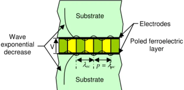
An innovative solution has been retained in order to answer to the need of high frequencies sources (RF until X band domain). These sources indeed need spectral purity, short-term stability and phase noise around the carrier wave. The purpose is to fabricate resonators based on the ultrasonic waves propagation through a waveguide. This resonator operates with a PPT structure inserted between two guiding substrates. A wave propagates without any acoustic losses and decreases exponentially in the structure (fig. 1). This definition is similar in these interface waves [2]. Nevertheless, the principle is substantially different for various reasons. First, the transduction structure corresponds to a layer in which ferroelectric domains have been artificially structured as developed in [3-4-5]. Classical interdigital transducers have been given up in this kind of structure because the bonding is difficult due to the electrode pattern. In this case, a polymer film is deposited between both substrates to be bonded in order to create an elastic link introducing important acoustic losses.
Figure 1. Scheme of the new concept waveguide based on PPT
B. Analysis of dispersion properties of this waveguide
We propose to closely investigate how to efficiently derive the dispersion curves and then to show at least for the elliptic mode of the waveguide the influence of the PPT geometry and the operating frequency on the mode properties. In that matter, we have considered the general shape of the waveguide symbolized in fig.2. We assume here a propagation between two silicon layers but the approach can be generalized to any guiding substrate. The period is arbitrarily fixed to 50 µm (i.e. width of each LiNbO3 domain set to 25 µm, poling ratio=0.5).
Figure 2. Scheme of PPT principle and generic shape for dispersion curve derivation
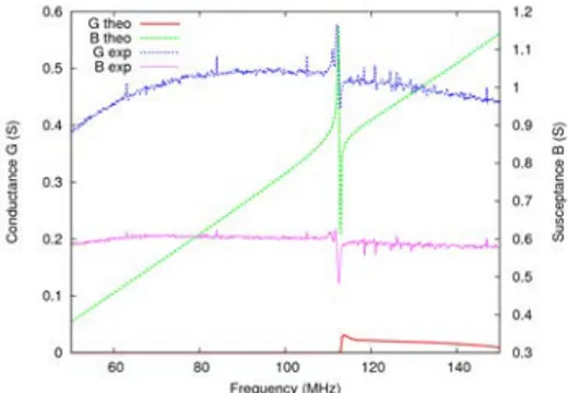
In Figure 3, we have plotted the theoretical admittance (conductance and susceptance) versus frequency for a thickness/period (h/p) ratio equal to 0.1 with 50 µm of period, in order to identify the main contribution corresponding to an elliptically shaped mode.
Figure 3. Harmonic admittance of the structure plotted in fig.2 for a thickness/period ratio equal to 0.1 with 50 µm of period
Once the mode identified, we follow the evolution of its resonance frequency and electromechanical coupling coefficient for h/p ratios ranging from 0.1 to 2, is plotted on fig.4.
(a) (b)
Figure 4. (a) Evolution of the elliptic mode synchronism frequency and (b) electromechanical coupling for small values of h/p ratio (ranging from 0.1 to
2 in our calculation) for different periods
The optimum point of the electromechanical coupling of this device depends of the transducer period (fig.4.a). In fact, the smaller the period, the weaker the electromechanical coupling. Besides, the electromechanical coupling approaches to a λac Electrodes p = λac Wave exponential decrease Poled ferroelectric layer Substrate Substrate V
maximum for a 50 µm period. At this point, the coupling is about 0.7%. When the period is smaller than 50 µm, the coupling decreases. The advantage to reduce the period size is to rise the wave celerity (fig.4.b). We can also observe that for a h/p ratio corresponding at an optimum of the electromechanical coupling, we find the maximum of the wave celerity. These operating points are particularly important as it conditions the possibility to improve the design reliability by choosing operation condition poorly affected by technology, which is a key point for any practical exploitation of the device. The next section shows the different technological steps of the fabrication of a Si/PPT/Si device.
III. FABRICATION AND CHARACTERIZATION OF THE NEW ACOUSTIC WAVEGUIDE: SI/THINNED PPT/SI
The analysis of the dispersion properties of a device constituted by Si/LiNbO3 PPT (λ=50 µm)/Si has shown a specific operating point for which a single wave is excited with a maximum electromagnetic coupling. This point is obtained for a h/p ratio of about 0.6 corresponding to a 30 µm thick LiNbO3 PPT. We will also show experimental results obtained with a thick layer of LiNbO3 in order to compare both devices. Technological steps checking the reliability of the concept using a thick PPT are described in [6].
A. Fabrication of the new waveguide
The fabrication of acoustic waveguides based on PPTs consists in bonding a silicon wafer on each side of the periodically poled wafer. In that purpose, the 500 µm thick Z cut lithium niobate wafer is poled and bonded on a (100) 3" doped silicon wafer using a wafer bonding technique developed in our group based on a metal-metal adhesion at room temperature promoted by a high pressure applied to the material stack (fig.7b). The study of the dispersion properties enables to define a specific configuration using a thinned PPT layer of about 30 µm. The LiNbO3 wafer thinning is achieved by home-made lapping and polishing techniques. After this step, the stack of Si(380 µm)/LiNbO3(20 µm) is bonded again on a doped silicon wafer with the same properties that the first one.
(a) (b)
Figure 5. (a) Flowchart which summarizes the different steps of fabrication (b) Double bonding of a 20 µm thick lithium niobate layer with
two silicon wafers using room temperature Au/Au bonding process
B. Characterizations and comparisons with theory
Two test vehicles have been achieved. The first one allows to check the reliability of the concept, using a Si (380 µm)/LiNbO3 PPT (500 µm)/Si (380 µm) structure. This structure is easier to fabricate because the PPT is not thinned. The second one based on a Si (380 µm)/LiNbO3 PPT (20 µm)/Si (380 µm) structure, enables to excite only one isolated mode. In fact, the final project is to create a resonator using this acoustic wave. The characterizations of both devices are obtained with a network analyzer. Figure 6 and 7 present the comparison between the measured responses of the implemented devices and the theoretical harmonic admittances calculated with our periodic finite element code. Measurements have been achieved successfully for the 50 µm period devices, as explained above. Since the implemented single-port test devices are quite long and almost behave as single port resonators, the comparison between measurement and harmonic admittance results makes sense.
Figure 6. Comparison between the test vehicle with 500µm thick LiNbO3 admittance and the calculated one
This plot points out the good agreement between both results. We find two main contributions corresponding to the elliptical mode (at 3800 m/s) and the longitudinal mode (at 6500 m/s). We can notice that the experimental admittance increases gradually. The main cause seems to be the wire length of the connection between the device and the support. This proves the feasibility of LiNbO3-based Silicon/PPT/Silicon devices.
Figure 7. Comparison between the test vehicle with 20 µm thick LiNbO3 admittance and the calculated one
This plot points out also the good agreement between both results. Only one contribution (except bulk waves) is exited (at 5500 m/s) by the PPT thinned and guided by the silicon. This wave corresponds to an elliptical isolated mode. As we have seen on the dispersion curve, the elliptical wave celerity rises when the thickness of the PPT decreases. In fact, the thinner the PPT, the higher the wave celerity because waves are accelerated by the silicon, which is the guiding material. The parasitic bulk waves seem to come from the electrode shape which is bigger than the transducer. Thanks the experimental admittance curve, the quality factor of the resonance and the electromechanical coupling can be calculated. We have found a Qf product of 1.1*1011 and a k² of 0.65%. As we have seen previously in the analysis part, there is a good agreement between the theoretical and experimental results.
For both devices, we have also measured the experimental admittance at different temperatures (fig.8). For the structure based on a 500 µm thick PPT, the theoretical and the experimental Temperature Coefficient of Frequency (TCF) are in the same order of magnitude at around -80 ppm/K. We can notice that the TCF is sensibly the same than the one of isolated LiNbO3 devices. For the second structure (20 µm thick PPT), the TCF is considerably smaller than the previous one. We found indeed a TCF equal to about -35 ppm/K. There is a good agreement between experimental and theoretical results. We can notice that the TCF is sensibly the same than the one of the silicon [7].
Figure 8. Theory/experiment comparison for the Temperature Coefficient of Frequency (TCF) for both test vehicles
So the waveguide concept based on a double silicon bonding on a thinned LiNbO3 PPT layer (about 20 µm) has been validated. Now, the purpose is to use the isolated wave excited to make a resonator for instance. Thus, in the next part, we expose different structures with impedance mismatches generating scattering effects.
IV. DIFFRACTION ANALYSIS
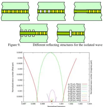
In this part, we propose some structures which would allow the reflection of the wave exited by the PPT. The exploitation of parametric adjustment methods enables, as we have shown in [1], to extract the typical characteristics of the PPT
propagation. Figure 9 presents different structures with impedance mismatches generating scattering effects. Figure 10 points out the stop band evolution for a structure based on a Si/10 µm thick PPLT/Si stack (no etched materials) for periods varying between 15 µm and 35 µm.
Figure 9. Different reflecting structures for the isolated wave
Figure 10. Stop band evolution for various PPLT periods based on the structure with integer reflection coefficient (γ) for a 10 µm thick layer So, we can notice that the first diffraction analysis point out a stop-band just with a Si/PPT/Si structure.
V. CONCLUSION
Si/PPLN/Si test vehicles, exhibiting a 50 µm period and a 20 µm thick ferroelectric layer, have pointed out the existence of an isolated mode operating at frequencies near 110 MHz. We have experimentally and theoretically demonstrated that the temperature coefficient of frequency of thinned LiNbO3 (20 µm) is smaller than the one of thick LiNbO3 (500 µm). This parameter has to be considered for radar applications. The diffraction analyses point out a stop-band just with a Si/PPT/Si structure. The corresponding parameters are found close to those of quartz (reflection coefficient magnitude between 0.5 and 1% for one period) with resonance occurring at the end of the stop-band. The addition of reflection structures, as etched patterns in the silicon or the ferroelectric substrates, plays a significant role in the efficiency of wave scattering.
ACKNOWLEDGMENT
This work was supported by the french DGA (Délégation Générale pour l’Armement) under grant#07-34-020.
REFERENCES
[1] S. Ballandras, R. Lardat, M. Wilm, Th. Pastureaud, A. Reinhardt, N. Champavert, W. Steichen, W. Daniau, V. Laude, R. Armati, G. Martin, “A mixed finite element/boundary element approach to simulate complex guided elastic wave periodic transducers”, accepted for publication in Journal of Applied Physics, 2008
[2] H. Majjad, D. Gachon, V. Laude, S. Ballandras, “Interface acoustic wave devices made by indirect bonding of lithium niobate on silicon”, Proc. of the IEEE US, 2006
[3] E. Courjon, J. Hauden, J. Masson, D. Gachon, L. Gauthier Manuel, W. Daniau, N. Bodin, S. Ballandras, “Pure longitudinal plate mode excited by poled domains transducers on LiNbO3”, Proc. of the IEEE IFCS,
2007
[4] E. Courjon, J. Hauden, P. Parruch, J. Masson, D. Gachon, L. Gauthier Manuel, W. Daniau, , N. Bodin, J.M. Triscone, S. Ballandras, “Fabrication of periodically poled domains transducers on LiNbO3”,
Proc. of the IEEE IFCS, Miami, 2006
[5] S. Ballandras, W. Daniau, B. Gautier, D. Hauden, M. Wilm, V. Laude, V. Ruch, S.Flambart, “A novel surface wave transducer based on periodically poled piezoelectric domain”, Proc of the IEEE EFTF-IFCS, 2003
[6] F. Bassignot, E. Courjon, G. Ulliac, T. Laroche, J. Garcia, S. Queste, J-P. Romand, S. Ballandras, “An acoustic waveguide using doubly-bonded silicon/thinned PPT/silicon structures for RF applications”, Proc. of the IEEE IUS, Rome, 2009
[7] Landolt-Börnstein, Numerical data and functional relationships in science and technology, Group III, Crystal and solid state physics, Vol. 11, K.H. Hellwege and A.M. Hellwege Eds., Springer-Verlag Berlin – Heidelberg – New York (1979)