HAL Id: tel-00261434
https://tel.archives-ouvertes.fr/tel-00261434v3
Submitted on 10 Oct 2008
HAL is a multi-disciplinary open access archive for the deposit and dissemination of sci-entific research documents, whether they are pub-lished or not. The documents may come from teaching and research institutions in France or abroad, or from public or private research centers.
L’archive ouverte pluridisciplinaire HAL, est destinée au dépôt et à la diffusion de documents scientifiques de niveau recherche, publiés ou non, émanant des établissements d’enseignement et de recherche français ou étrangers, des laboratoires publics ou privés.
Cryogenic AFM-STM for mesoscopic physics
Hélène Le Sueur
To cite this version:
Hélène Le Sueur. Cryogenic AFM-STM for mesoscopic physics. Condensed Matter [cond-mat]. Uni-versité Pierre et Marie Curie - Paris VI, 2007. English. �tel-00261434v3�
Hélène le Sueur
Quantronics Group
SPEC
Electronic spectroscopy based on electron tunneling gives access to the electronic Density of States (DoS) in conductive materials, and thus provides detailed information about their electronic properties.
During this thesis work, we have developed a microscope in order to perform spatially resolved (10 nm) tunneling spectroscopy, with an unprecedented energy resolution (10 µeV), on individual nanocircuits. This machine combines an Atomic Force Microscope (AFM mode) together with a Scanning Tunneling Spectroscope (STS mode), and functions at very low temperatures (30mK). In the AFM mode, the sample topography is recorded using a piezoelectric quartz tuning fork, which allows locating and imaging nanocircuits. Tunneling can then be performed on conductive areas of the circuit.
With this microscope, we have measured the local DoS in a hybrid Superconductor-Normal metal-Superconductor (S-N-S) structure. In such circuit, the electronic properties of N and S are modified by the superconducting proximity effect. In particular, for short N wires, we have observed a minigap in the DoS of the N wire, independent of position. Moreover, when varying the superconducting phase difference between the S electrodes, we have measured the modification of the minigap, and its disappearance when the phase difference equals π.
Our experimental results for the DoS, and its dependences (with phase, position, N length) are quantitatively accounted for by the quasiclassical theory of superconductivity. Some predictions of this theory are observed for the first time.
C
R
Y
O
G
E
N
IC
A
F
M
–
S
T
M
F
O
R
M
E
S
O
S
C
O
P
IC
P
H
Y
S
IC
S
le
S
u
e
u
r
Cryogenic AFM-STM
for
mesoscopic physics
2007
THESE DE DOCTORAT DE
L’UNIVERSITÉ PARIS 6 – PIERRE ET MARIE CURIE
Spécialité
Physique des Solides
Présentée par Hélène le Sueur
pour obtenir le grade de
DOCTEUR de l’UNIVERSITÉ PIERRE ET MARIE CURIE
Sujet de la thèse :
Développement d’un AFM-STM pour la spectroscopie électronique haute résolution de nanostructures et application à la supraconductivité de proximité
soutenue le 21 septembre 2007
devant un jury composé de
M Marco APRILI
M Claude CHAPELIER rapporteur
M Juan Carlos CUEVAS rapporteur
M Daniel ESTEVE directeur de thèse
M William SACKS
This thesis can be downloaded as a pdf file at:
http://www-drecam.cea.fr/drecam/spec/pres/quantro/qsite/index.htm
or
http://tel.archives-ouvertes.fr/
COVER:
The front cover shows an AFM image of a small circuit fabricated by electronic lithography and double angle evaporation, comprising a 350 nm long, 30 nm thick silver wire (colorized in orange) and a 60 nm thick aluminium half loop (dark grey). This structure has been imaged using an atomic force sensor, and tunneling spectroscopy was subsequently performed at several positions. Curves on the background are tunneling spectra measured for different values of the superconducting phase difference across the normal wire (at the location of the tip represented on the AFM image).
The graph on the backside of the cover is a 3D plot of the predicted local density of states along a 1D S-N-S structure, with a normal wire length L = 1.4 ξ (corresponding to 350 nm), and perfect interfaces.
R
EMERCIEMENTS
Ce fût un réel plaisir pour moi de travailler au Service de Physique de l’Etat Condensé. Je ne parle pas ici du seul groupe Quantronique, car ce sont réellement le rassemblement en un lieu unique d’autant de compétences diverses et leur prompte disponibilité qui m’ont donné la chance inouïe de mener à bon terme ce projet.
Tout d’abord, un grand merci à Eric Vincent qui m’a soutenue dans toutes mes demandes auprès du CEA, et m’a ainsi permis de rester parmi vous le temps nécessaire à la réalisation de notre première expérience de physique mésoscopique : quel bonheur ! Merci à ceux qui ont rendu cela possible, par leur intervention à divers niveaux : Louis Laurent, Philis Livanos, lors de mon entrée au SPEC, Didier Normand lors de la prolongation de mon contrat CFR, Sandrine Thunin et Nathalie Royer dans mes diverses démarches administratives.
Merci infiniment à Daniel Esteve, mon directeur de thèse, pour avoir appuyé sans réserve ma candidature, et tout ce qui s’en est suivi : Travailler avec un « chef » comme toi est un enrichissement extrême, tant pour ton recul sur la compréhension des phénomènes envisagés, que pour ton esprit pratique qui nous permet de parvenir plus vite (et mieux bien sûr !) au résultat souhaité… Et puis tu n’es pas chef pour rien : ce don d’ubiquité qui te permet de consacrer à tous les projets simultanément la même attention exclusive force sincèrement l’admiration !
J’espère avoir mérité toute la confiance que m’a accordée Philippe Joyez en me laissant la responsabilité de porter avec lui son projet de recherche, à ses débuts lors de mon arrivée dans le groupe. Ma seule gratitude ne peut exprimer justement tout ce que tu as fait pour moi car tu m’as fait vivre durant cette thèse une expérience de recherche inoubliable : construire une manip’ entière depuis la racine, l’élaborer pas par pas, et la faire marcher pour en tirer des mesures de premier ordre ! Quel thésard peut rêver mieux ?
Bien entendu une telle entreprise n’aurait pu aboutir sans le soutien technique de nombreuses personnes. Sans les compétences de Pascal Senat, les pièces du microscope seraient probablement usinées de travers, et cette mécanique si délicate n’aurait jamais fonctionné. Pief Orfila, non content de gérer la logistique du groupe ainsi que l’installation et le bon fonctionnement de la majorité des machines de nano-fabrication au SPEC, a de plus aménagé notre labo de manière astucieuse et confortable. Jean-Claude Tack a été d’une grande disponibilité pour l’usinage d’un bon nombre de pièces de câblage. Grâce à Michel Juignet, qui m’a initiée aux machines d’atelier, j’ai pu usiner moi-même –avec les conseils de Pascal-
quelques pièces du microscope. Je remercie chaleureusement toutes ces personnes pour leur aide précieuse.
Le réfrigérateur que nous utilisons pour faire l’expérience présentée dans ce manuscrit est un modèle construit par Air-Liquide, qui a présenté dès son achat de nombreux dysfonctionnements. Ce réfrigérateur a été envoyé en réparation avant le début de ma thèse, et n’est revenu qu’au milieu de la 2è année, en raison des difficultés rencontrées pour le réparer. Je tiens à remercier chaudement le personnel du CRTBT qui s’est attaché à ce travail difficile et peu gratifiant, en sus de leur taches personnelles. Le travail bénévole de Thomas Prouve, un étudiant en thèse, et Lionel Germani, un technicien cryogéniste m’aura permis -malgré le retard pris- d’utiliser le microscope que j’avais construit à des fins de recherche. Patrick Pari a aussi contribué à cette réparation puisqu’il a levé le tout dernier problème de cryogénie, nous permettant de récupérer ce réfrigérateur tant attendu pour commencer à le câbler. Patrick Pari continue, avec Mathieu de Combarieu et Philippe Forget, le groupe de cryogénie du SPEC, de nous aider à améliorer le fonctionnement du réfrigérateur. Merci à eux !
Faire de la physique dans le groupe Quantronique est en soi une chance, tant pour l’éclectisme que pour l’effervescence scientifique qui y règnent. Difficile de passer quatre années au contact de ses membres sans être contaminé par la passion qui les anime…
Denis Vion d’un enthousiasme constant pour mes divers balbutiements en montage de manip’, et d’un dévouement exceptionnel pour améliorer mon discours de soutenance : merci de ton soutien dans ces moments difficiles, et merci d’avoir pris sur toi tout mon stress le jour J, comme en témoignaient tes grimaces pendant mon exposé!
Hugues Pothier sans qui la salle café serait jonchée de miettes de gâteau. Cette seule description est un peu réductrice je l’avoue : il faut aussi noter la finesse de ses explications physiques qui savent aborder la problématique de manière simple et limpide en utilisant les bonnes images. Merci à toi de m’avoir introduite aux subtilités de l’effet de proximité, et m’avoir évité de tourner en rond trop longtemps pour choisir les bons paramètres d’expérience.
J’ai beaucoup apprécié les compétences et l’exigence de Cristiàn Urbina, dans de multiples domaines et notamment en matière d’écriture anglaise. Merci pour ta relecture attentive de mon manuscrit et tes corrections qui sont sûrement responsables des compliments que j’ai reçus en ce sens.
Merci à Patrice Bertet, nouveau membre permanent du groupe, pour ses idées originales en provenance du grand nord, sa grande capacité d’écoute et de conseil, et sa contenance qui contraste avec l’impertinence du groupe ! A bientôt à La tuile à loup…
Je souhaite une bonne continuation aux thésards et post-docs que j’ai côtoyés durant mon séjour : Martin Chauvin et Peter Vom Stein, le premier duo P08, responsable de nombreuses soirées pizza / vidéo-projecteur qui m’ont souvent remonté le moral ! Anne Anthore et Ronald Cron, qui ont partagé durant quelques mois ces soirées avec nous, Benjamin Huard et Maria-Luisa Della-Rocca dignes successeurs de Peter et Martin, et Quentin Le Masne, qui prend maintenant la relève avec autant de punch. Bon vent aux manipulateurs de Q-Bit : Eddy Collin, Grégoire Ithier, Nicolas Boulant, François Nguyen, François Mallet et Agustin Palacios : puissent les suivants animer la P4 team aussi bien que vous !
J’ai apprécié de passer ce temps en compagnie des divers groupes du SPEC : les magnétiseurs, le groupe bruitonique (le sous-sol humide est-il toujours propice à la culture des blagues graveleuses ?), les LEMuriens, les turbulents… thésards, post-doc ou permanents avec qui il était toujours agréable d’échanger.
Je remercie également les différentes personnes qui m’ont accordé leur disponibilité et m’ont fait partager leurs connaissances de manière toujours très sympathique : merci tout particulièrement à Juan Carlos Cuevas, Wolfgang Belzig, Elke Sheer, Terö Heikkilä, Mathias Eschrig, Takis Kontos, Audrey Cottet, Anne Anthore, Sophie Guéron, Hélène Bouchiat, Francesca Chiodi pour nos échanges très instructifs sur l’effet de proximité, à Hervé Courtois, Gabino Rubio-Bollinger, Nicolas Agrait, Herman Suderow et Olivier Klein pour avoir partagé avec moi leur expérience sur la microscopie, à Marcelo Goffman et Roland Lefebvre pour m’avoir fourni des échantillons lors des tests initiaux du microscope.
Je suis très reconnaissante envers Juan Carlos Cuevas, Claude Chapelier, Marco Aprili, William Sacks, et Christian Schönenberger d’avoir accepté de faire partie de mon jury.
Enfin, mes pensées vont vers tous ceux qui m’ont épaulé durant cette thèse et ont rendu ces années plus agréables. Je pense tout particulièrement à mon père Henri, ma mère Marie-Claude, et à Florence et Benjamin, ma famille au sens large, qui accompagnent mes réussites et mes échecs depuis le début.
Je regrette déjà cette dualité d’une grande profondeur d’esprit avec des discours irrévérencieux, qui caractérise le groupe Quantronique, et souhaite sincèrement pouvoir prolonger dans l’avenir nos discussions passionnantes -de tout ordre- et notamment celles sur les macarons !
T
ABLE
O
F
C
ONTENTS
1 General introduction --- 12
1.1 Tunneling spectroscopy ...16
1.2 Spatially resolved measurement of the LDOS with a combined AFM-STM...19
1.3 An AFM-STM in a table-top dilution refrigerator...22
1.4 Benchmarking tunneling spectroscopy ...23
1.5 An experiment on the proximity effect in S-N-S structures ...25
1.6 Perspectives...31
1.6.1 Proximity effect in ballistic 1D systems... 31
1.6.2 Proximity effect in a 2D system ... 31
1.6.3 Spin injection and relaxation in superconductors ... 32
1.6.4 Energy relaxation in quasi-ballistic (“Superdiffusive”) structures... 32
2 Design, Fabrication and Operation of the Microscope --- 34
2.1 The microscope structure ...36
2.1.1 General description ... 36
2.1.2 Materials and construction ... 37
2.1.2.1 Material selection ... 37 2.1.2.2 Mechanical structure... 39 2.1.2.3 CAD Design... 39 2.1.2.4 Assembly ... 43 2.1.2.5 Plating of titanium ... 44 2.2 Piezoelectric actuators ...45
2.2.1 The piezoelectric effect ... 45
2.2.1.1 General mathematical description of piezoelectricity... 45
2.2.1.2 Practical equations for piezoelectric devices ... 46
2.2.2 Practical piezoelectric materials ... 47
2.2.2.2 Quartz crystal ... 47
2.2.2.3 PZT piezoelectric material ... 48
2.2.2.3.a Description ... 48
2.2.2.3.b PZT ceramics: poling and depoling... 48
2.2.2.3.c PZT actuators shapes and functioning ... 49
2.2.2.3.d Imperfections of PZT ceramics: drift and hysteresis ... 52
2.2.2.3.e PZT ceramics at low temperature... 53
2.2.3 The piezoelectric tube ... 53
2.2.3.1 Poling procedure... 54
2.2.3.2 Calibration at high and low temperatures ... 54
2.3 Coarse positioning and indexing ...56
2.3.1 Design & principle... 56
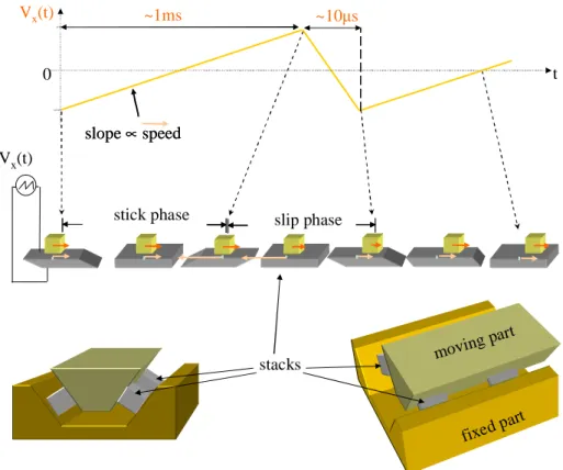
2.3.1.1 Stick-slip motion ... 56
2.3.1.2 Electrical requirements ... 57
2.3.1.3 Mechanical performance of the motors ... 58
2.3.1.4 Inertial vs. non-inertial stick-slip motion... 59
2.3.2 Position indexing ... 59
2.3.2.1 Design... 59
2.3.2.2 Resolution and accuracy of the capacitive position sensors... 60
2.3.2.3 Practical implementation... 61
2.3.2.4 Testing actuators and sensors. ... 63
2.4 The atomic force sensor...66
2.4.1 implementing AFM sensors at low temperature ... 67
2.4.1.1 Optical sensors ... 67
2.4.1.2 Electrical sensors ... 68
2.4.2 Quartz Tuning Fork (TF)... 69
2.4.2.2 Tuning forks for atomic force microscopes ... 69
2.4.2.3 Oscillating modes of the tuning fork... 72
2.4.2.4 Basic analysis of a tuning fork: 1 Degree-of-Freedom harmonic oscillator model... 73
2.4.2.4.b Mechanical analysis ... 74
2.4.2.4.c Tip-sample interaction... 75
2.4.2.5 Discussion of the 1-DOF model ... 77
2.4.2.6 Model of a tuning fork as three coupled masses and springs ... 78
2.4.2.6.b Free dynamics of the 3-DOF model ... 79
2.4.2.6.c Balanced tuning fork: the unperturbed modes... 81
2.4.2.6.d Broken symmetry: a perturbative analysis ... 81
2.4.2.6.e Discussion ... 83
2.4.2.7 Estimating characteristics of the connecting wire for preserving the tuning fork balance ... 84
2.4.2.8 Measuring the oscillator parameters... 86
2.4.2.8.b Resonance curves during the setup... 87
2.4.2.8.c Capacitance compensation... 88
2.4.2.8.d Extracting the resonator parameters ... 88
2.4.3 Force measurement ... 89
2.4.3.1 Typical forces on the atomic scale ... 90
2.4.3.2 “Force” measurements: sensor stability and sensitivity... 91
2.4.3.3 “Force” measurements: detection schemes... 93
2.4.3.4 Phased locked loop detection... 95
2.4.3.5 Feedback loop in imaging mode ... 97
2.4.3.5.b Optimizing AFM imaging ... 98
3 Experimental techniques --- 100
3.1 A dilution refrigerator well adapted for a local probe microscope...102
3.1.1 Functioning of the inverted dilution refrigerator ... 102
3.1.2 (not so good) Vibrations in dilution refrigerator... 105
3.1.3 Living with vibrations... 108
3.1.4 Possible improvements ... 109
3.2 Wiring a microscope for very low temperature experiments...110
3.2.1 Thermal load ... 110
3.2.2 Low level signals and low noise requirements ... 112
3.2.3 Filtering... 112
3.2.3.1 Necessity of filtering... 113
3.2.3.2 Why filtering all the lines? ... 113
3.2.3.3 Propagation of thermal noise in networks ... 114
3.2.3.4 Filtering technique... 118
3.2.3.5 Fabrication ... 120
3.2.3.6 Electromagnetic simulations of the filters. ... 125
3.2.3.7 Filter attenuation... 128
3.2.3.8 Analysing the full setup ... 129
3.2.3.9 Experimental validation of the filtering setup... 131
3.2.3.10 Article reprint: microfabricated filters... 131
3.2.4 Tunneling spectroscopy ... 137
3.2.4.1 Tunneling spectroscopy measurements ... 137
3.2.4.2 Data acquisition setup ... 139
3.2.4.3 Article reprint : Tunnel current pre-amplifier ... 143
3.3 Fabrication techniques ...149
3.3.1 Tip fabrication ... 149
3.3.1.1 Electrochemical etching... 149
3.3.1.2 Tungsten tips ... 151
3.3.1.3 Niobium tips... 156
3.3.1.4 In-situ tip cleaning ... 156
3.3.1.5 Tip damages and tip reshaping ... 157
3.3.2 Sample preparation ... 160
3.3.2.1 Position encoding grid ... 160
4 Mesoscopic superconductivity --- 166
4.1 Introduction to proximity effect...167
4.2 Theoretical description of Proximity Effect...168
4.2.1 Inhomogeneous superconductivity ... 168
4.2.2 The Bogolubov – de Gennes equations... 168
4.2.3 Theoretical description of the proximity effect in diffusive systems at equilibrium ... 169
4.2.3.1 Electronic Green functions... 169
4.2.3.2 Green functions in the Nambu space... 169
4.2.3.3 Quasiclassical Green functions in the dirty limit - Usadel equation ... 170
4.2.3.4 Properties of the Green function elements - Physical quantities ... 170
4.2.3.5 Boundary conditions ... 172
4.2.4 Parameterization of the Green functions ... 174
4.2.4.1 θ, φ parameterization ... 174
4.2.4.1.b Nazarov's Andreev circuit theory... 175
4.2.4.2 Ricatti parameterization ... 176
4.2.4.2.a Advantages of this parameterization... 177
4.2.4.2.b Ricatti parameters in reservoirs... 177
4.2.4.2.c (Dis-)Continuity of Ricatti parameters at interfaces ... 178
4.2.5 Spectral quantities in the Ricatti parameterization... 178
4.2.6 A word on the non-equilibrium theory... 179
4.3 Solving the Usadel equations numerically ...180
4.3.1 Reduction of the problem dimensionality ... 180
4.3.2 Specifying the 1-D problem ... 181
4.3.3 Solving strategy - self-consistency ... 182
4.3.4 Implementation details... 182
4.4 General results on proximity effect in SNS structures ...186
4.4.1 “Minigap” in the DOS... 186
4.4.2 Inverse proximity effect – Pairing amplitude and pairing potential ... 187
4.4.2.2 Self-consistency... 188
4.4.3 Role of interfaces... 190
4.4.4 Dependence of the minigap on N size... 191
4.4.5 Phase modulation of the proximity effect... 192
4.5 SNS systems viewed as scattering structures ...193
4.6 An STM experiment on the proximity effect ...195
4.6.1 Sample geometry ... 195
4.6.2 Implementation of the experiment ... 196
4.6.2.1 Achieving a good phase bias ... 196
4.6.2.1.a Kinetic inductance correction... 197
4.6.2.1.b Circulating currents correction... 197
4.6.2.2 Sample fabrication... 198
4.6.2.3 Overview of the measured SNS structures ... 199
4.6.3 What do we measure? ... 200
4.6.4 Density of states in a long SNS structure ... 201
4.6.5 Density of states in a short SNS structure ... 202
4.6.5.1 position dependence... 202
4.6.5.2 phase dependence ... 206
4.6.5.2.b Phase calibration... 209
4.6.5.2.c minigap as a function of phase... 209
4.6.5.3 Is the Al electrode affected by the applied field? ... 210
4.6.6 Density of states in a medium-size SNS structure ... 212
4.6.6.1 Intermediate regime ... 212
4.6.7 Comparison with theory... 213
4.6.7.1 Parameters entering the theory ... 213
4.6.7.2 Comparison with theoretical predictions ... 216
4.6.7.2.a Determination of the parameters ... 216
4.6.7.2.b Position dependence... 219
4.6.7.2.c Phase dependence ... 221
4.6.7.2.d Length dependence ... 222
4.6.7.3 Summary of the fitting parameters... 223
4.6.7.4.a Positioning accuracy... 224
4.6.7.4.b Energy resolution... 224
4.6.7.5 Model limitations... 225
4.6.7.5.a Depairing... 225
4.6.7.5.b Self consistent treatment of the proximity effect ... 225
4.6.7.5.c 1-D model of the NS interface ... 225
4.6.7.5.d Transverse extension, sample geometry ... 226
4.6.8 Article reprint: proximity effect in S-N-S structures... 226
4.7 Conclusions ...233
4.7.1 Further experiments ... 233
4.7.1.1 Out of equilibrium proximity effect ... 233
C
HAPTER
1
1
1
G
G
E
E
N
N
E
E
R
R
A
A
L
L
I
The ability to combine in a given nanostructure materials with different electronic properties such as normal metal conductors, magnetic or superconducting electrodes, conductors of reduced dimensionality, single molecules,… has opened new perspectives in mesoscopic physics and nanophysics. The operation of field-effect transistors based on single gated carbon nanotubes [1], and the production of spintronic devices in which the orientation of a single nano-size magnetic domain controls (or is controlled by) an electrical current [2], exemplify the progress achieved during the recent years. A wide range of electronic phenomena have been found in the numerous combinations of materials explored: superconductivity in nanostructures made of both superconducting and non-superconducting materials, Kondo effect in quantum dots connected to bulk Fermi reservoirs [3], spin and charge transport in spintronic devices… Understanding the behaviour of such heterogeneous nanostructures with competing electronic orders remains a major challenge in mesoscopic physics.
At an interface between two different materials, variations of the electronic properties often occur on short length-scales. Local probing of electronic spectroscopy, with a good spatial resolution, is therefore necessary. Besides, such local spectroscopic measurements are often more direct tests of microscopic models of the system than transport measurements are. Moreover, the energy range over which these effects appear is often quite small (typically ~1 meV and down to a few 10 µeV), compared to, for instance, the thermal energy at room temperature (kBT~30 meV). It is thus mandatory to cool the experiments down to very low temperatures, in the millikelvin range, first to make these phenomena observable, as well as to measure them without thermal blurring.
Many different kinds of spectroscopies using electron, ion or photon beams, such as Electron Energy Loss Spectroscopy or photo-emission, can be used to perform a local electronic characterisation. However, their spatial resolution is often poor, and the probed energy range (eV or higher) is larger than the relevant one for mesoscopic physics. In order to obtain spatially resolved information, and to probe small energies, various types of scanning probe microscopies have been developed. Two main operation modes, electronic or optical, can be used to probe either electronic or electro-magnetic spectroscopies. In the electronic mode, a very sharp conducting tip is scanned above the sample surface, while the conductance between the tip and the sample is recorded. This method used in the low conductance regime measures the ability to inject electrons from the tip to the sample. It is called “tunneling spectroscopy”. In the optical mode, an optical fiber with a very narrow apex is used to collect optical photons from the sample surface, to probe for instance the electromagnetic density of
states [4]. Combined electronic-optical systems operating both in excitation and detection modes are also feasible [5, 6].
The aim of this thesis work was precisely to design, fabricate and operate an apparatus able to probe the electronic ordering in isolated conducting nanostructures using tunneling spectroscopy, in the low energy range suitable for mesoscopic physics.
For this purpose, a microscope with both imaging and local electron spectroscopy abilities was built and mounted in a dilution refrigerator.
1.1
Tunneling spectroscopy
Tunneling spectroscopy was experimentally introduced in 1960 by Giaever in the particular case of tunneling of quasiparticles between a superconductor and a normal metal, using planar junctions [7]. In 1981, Binnig and Rohrer developed the Scanning Tunneling Microscope, providing condensed matter physics with a tool able to perform spatially resolved electronic spectroscopy [8].
Although the basic theory of tunneling dates back to the early days of quantum mechanics [9], the interpretation of most tunneling measurements relies on the tunneling-Hamiltonian formalism introduced in the early 1960s, in particular by Bardeen [10, 11], and by Cohen, Falicov and Philips [12]. In this framework, two independent systems are linked by a Hamiltonian of the form
† , , . . =
∑
+ T a b a b a b H T c c h c , (1.1)which transfers single electrons between states in electrode a and states in electrode b, and where c+ and c are the creation and annihilation operators of single particle states in the electrodes, and , = 2ℏ2
∫
Ψ ( ) Ψ ( )*a b m b a
T r r dr is the tunneling matrix element between a states and b states1.
In the case of tunneling from a sharp STM tip, one expects the tunneling process to be essentially local, limited to the close vicinity of the tip apex. Indeed, Tersoff and Hammann [13] have shown that, assuming the tip apex can be modelled by a sphere, the tunneling matrix elements Ta b, are such that
( )
2 2
, ∝ Ψ
a b b c
T r , (1.2)
where Ψb
( )
rc is the value of the sample single-particle wave function b at the center (rc) ofthe tip apex. For the sake of simplicity, the contact point between tip and sample is assimilated to rc.
From this result, one easily derives a perturbative expression for the tunneling current within the linear response theory, involving only quantities in the electrodes at rc [13]:
1
We neglect here the possible coupling of tunneling electrons to collective electromagnetic or phonon modes which would give rise to inelastic processes that modify the tunneling current. This is generally valid when dealing with “good” metallic electrodes having low electromagnetic impedance, and at voltages below a few mV.
2 2
4
( )=
∫
( − )− ( , ) ( − ) ( , )ℏ tip sample c tip sample c
e τ
I V dε f ε eV f r ε ρ ε eV ρ r ε , (1.3)
where ρtip sample, denote the local electronic densities of states (LDOS) in the tip, and in the
sample at the contact point r and c ftip sample, ( )ε are the local energy distribution functions - or
occupation number of electronic states - in the electrodes (which reduce to Fermi functions at thermal equilibrium). τ is the average value of the tunneling matrix elements Ta b, .
Expression (1.3) can be easily understood in terms of a balance of tunneling events in both directions from occupied to empty states. It is the usual basis for analysing local tunneling spectroscopy experiments and it is worth noticing and stressing that, to date, most STM spectroscopic measurements have been successfully and often accurately analysed within this rather simple Tersoff and Hammann picture. Thus, deviations from this description due to tip shape effects or tip-sample interactions are generally negligible.
As we will now show, under favourable conditions, one can disentangle the factors contributing in (1.3), thereby gaining knowledge of local spectral functions in the electrodes. The case when both tip and sample are Fermi liquids with arbitrary densities of states is depicted in Fig. 1.1, where it is further assumed that both electrodes are at thermal equilibrium.
When one wants to probe the LDOS in the sample, one uses a tip where the density of states can be assumed as constant over the probed relevant energy range (see Fig. 1.2). This is the case for normal-metal tips, in the energy range suitable for mesoscopic physics (meV). The LDOS plays a major role in the knowledge of physical properties of the system. It is formally amenable to calculation once the Hamiltonian of the system is known; for instance it can be expressed as a retarded Green function for electrons.
In order to determine the local energy distribution function in a sample, one rather uses a superconducting tip1. In this case the sharp BCS singularity [14] of the tip DOS probes the energy distribution discontinuities. In this mode, out-of-equilibrium situations can be probed, giving access to fast dynamics inside the structure. Out-of-equilibrium distribution functions can in principle be calculated from Green functions, but here within the Keldysh formalism.
1
It is possible to access energy distribution of electrons using a normal tip in a high impedance environment, using the Zero Bias Anomaly (ZBA) induced in the density of states of the tip by dynamical coulomb blockade [15]. However, the ZBA has a less sharp singularity, compared to the BCS singularity (which is nearly a delta peak) and is thus a less efficient probe.
fSample(ε) ρSample(ε) ftip(ε) ρtip(ε) I(V) Ta,b a b T S V
Fig. 1.1 On the left are shown side to side the densities of states of arbitrary probe (ρtip) and sample (ρsample) as a function of energy (vertical axis). The filling of states (f between 0 and 1) is represented in plain color (orange for the tip, blue for the sample). Fermi levels are shifted by the voltage bias applied to the junction. The current flowing through a tunnel junction between the tip and the sample involves the convolution product of spectral functions ρ and f of the electrodes (see expression (1.3)). The right panel exemplifies tunneling from a state a in the tip into a state b of the sample with a coupling Ta,b.
fsample(ε) ρsample(ε) fN(ε) ρN(ε)=cst ~3.5kBT ρsample(ε) fS(ε) fsample(ε) ρBCS(ε) (a) (b)
( )
BCS samplef
V
I
V
V
ρ
∂
∝
∗
∂
∂
∂
BCS Re 2 2 ε ρ = ε − ∆ ( )
sample Nf
I
V
V
V
ρ
∂
∂
∂
∝
∗
∂
εFFig. 1.2 Tunneling spectroscopy with normal metal (a), and with superconducting tips (b). (a) When
ρtip(ε) is featureless (normal metal), the differential conductance, which is the derivative of current with respect to applied voltage, gives direct access to the local density of states in the sample, with a maximal resolution given by the sharpness of the Fermi-Dirac function, involving the temperature T in the tip (note that temperatures are not necessarily equal). (b) With a superconducting tip, tunneling gives access to the energy distribution function in the sample, provided ρsample(ε) is constant at Fermi level, using a deconvolution procedure. Experimental techniques about the DOS measurement are discussed in chapter 3.
1.2
Spatially resolved measurement of the LDOS with a
combined AFM-STM
Scanning Tunneling Microscopes have been exploited for spectroscopy purposes since the very beginning. The visualization by D. Eigler et al. of a quantum corral for electronic surface states delimited by atoms added on a crystalline surface is one famous example [16, 17]. Despite its obvious interest, scanning tunneling spectroscopy has however not been much used to probe nanostructures. There are two main reasons for this:
• Circuits are designed on insulator:
Most of nanostructures are fabricated on an insulating substrate, on which an STM cannot be operated: as soon as the tip hovers on an insulating part, tunneling current drops to zero, just as if it were far from the sample surface. Therefore, the feedback mechanism lowers the tip to reach the target tunnel current, unavoidably resulting in a “tip crash” most dreaded by all STM users. In order to perform local probe measurements on such samples, one needs to resort to another type of local probe. Atomic Force Microscopy (AFM) is the most obvious choice since it has topographic imaging capability with high spatial resolution, quite independently of the sample properties, in particular of its conductivity.
• Circuits are small compared to the chip:
On a given sample of macroscopic size, there is often one or a few nanostructures connected to the outside by large bonding pads. Fig. 1.3 shows as an example one of the samples measured during this thesis work. The area of interest has a characteristic size of a few microns, located at the center of a 5x5 mm2 chip. Reliably bringing the local probe of a microscope on top of the nanostructure requires precise mechanical alignment capabilities of the local probe with respect to the sample in all three dimensions.
In order to perform spatially resolved tunneling spectroscopy on nanostructures, and to cope with the first point above, we have built a near-field microscope having a combined Atomic Force and Tunneling probe, which can be used in either mode. In AFM mode, topographic images of the sample can be obtained whatever its electrical properties. The STM mode is primarily used to measure LDOS at desired locations. This dual mode sensor is shown in Fig. 1.4, and will be described in chapter 2. It is based on a tuning fork normally used as the time-base resonator in wristwatches. Such a tuning fork resonator is made of quartz, a
piezoelectric material, which allows easy, low power, electrical excitation and detection of its mechanical resonance (~32 kHz) and is thus well adapted for very low temperature experiments. This tuning fork is equipped with a metallic probe tip attached to one arm. The attractive or repulsive interaction between the tip and the sample surface affects the tuning fork resonance. A feedback system regulating the tip-to-sample distance is used to maintain a constant target resonance frequency while the tip scans the sample surface. This way, one can form topographic images of the sample surface. Once the area of interest is located, switching to the STM mode, and performing tunneling spectroscopy at precise locations is then possible without endangering the tip. The small wire connected to the tip carries the tunnel current, and allows tip biasing with respect to sample.
To cope with the second point, we incorporated in our microscope means of precisely displace the sensor with respect to the sample in all three directions of space over large distances (several mm). This motion is performed by piezoelectric actuators based on stick-slip motion. To compensate for the lack of reproducibility of these actuators, and since operation at very low temperatures does not allow visual access, we fitted our microscope with position sensors. We further designed the samples so as to help us rapidly locate the nanostructure of interest. All these features are described in details in chapters 2 and 3.
Fig. 1.3 A typical sample made on a 5 mm chip by standard e-beam lithography and metal deposition, is glued by silver paint on a sample holder, and bonded to contacts for transport measurements. The Moiré patterns that can be seen on a 3 mm field in the center of the sample are position encoding marks for the microscope. For the description of the encoding see chapter 3.
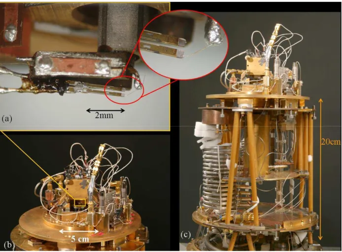
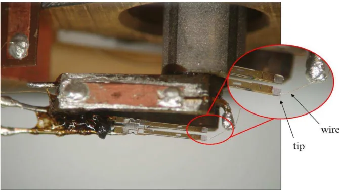
Fig. 1.4 (a) Picture of the combined AFM-STM probe, attached to the end of a piezoelectric scanning tube. A sharp metallic tip (inset) is glued at the end of the lower arm of the tuning fork. The fork senses the interaction between tip and sample, which allows to image topography with a precision mainly limited by the shape of the tip apex. The tip is electrically connected by a thin wire to a filtered measuring line for performing tunneling spectroscopy. (b) Picture of the microscope mounted and wired on the top plate of an inverted dilution refrigerator. (c) Ensemble view of the dilution refrigerator, model SIONLUDI designed by A. Benoit from the CNRS (Grenoble). This fridge cools the experiment down to 30mK in about 8 hours.
1.3
An AFM-STM in a table-top dilution refrigerator
Mesoscopic physics experiments are often performed at low temperature since the characteristic energy scales of the investigated phenomena are generally small: for instance, for pure metals superconductivity occurs only below a critical temperature of the order of 1 -10 K. Moreover, electron coherence effects tend to disappear as temperature rises, due to incoherent scattering by phonons… In general, a temperature higher than the relevant energy scale blurs the measurement: as explained in Fig. 1.2, the energy resolution of tunneling spectroscopy is ultimately limited by the temperature at which the experiment is performed. However, to reach this ultimate limit, or even approach it, it is not enough to cool the sample and the microscope. It is also necessary to carefully thermalize and filter all the lines connected to the sample so that not only the external noise (either noise from room-temperature apparatus, or ambient noise), but also the Johnson-Nyquist noise arising from all dissipative elements placed in these lines at temperatures higher than the sample temperature, are suitably attenuated.
For these reasons, the microscope was placed in thermal contact with the mixing chamber of a dilution refrigerator with a base temperature of about 30 mK and the wiring of the experiment was carefully designed so as to benefit from the low operating temperature. In particular, special filters were designed, fabricated and installed on every line, and a new type of tunnel current preamplifier was designed. The fabrication and setup of the full apparatus is described in chapter 3.
We use a table-top dilution refrigerator, developed by Alain Benoit from the Centre de Recherche sur les Très Basses Températures (CRTBT), and which has the advantage of being of comfortable use and suitable for a microscope such as ours. All leak-tight seals are situated at room temperature, and the whole fridge and the experiment are placed inside the same vacuum chamber. This fridge is not surrounded by a cryostat filled with liquid helium, but it operates with circulating liquid helium fed from a slightly pressurized storage Dewar placed underneath. Although a couple of groups are successfully using this type of dilution refrigerator with STMs, we found our own fridge, which was actually fabricated by Air Liquide, to be plagued by internal vibrations, presently forbidding normal tunnel vacuum STM operation. We could nevertheless perform very stable tunneling spectroscopy by bringing the tip in mechanical contact with the sample, through a thin insulating layer grown on the sample surface.
1.4
Benchmarking tunneling spectroscopy
A convenient benchmark for tunneling spectroscopy is the measurement of the DOS of a BCS superconductor with a normal metal tip, as shown in Fig. 1.2. Ideally, the measured conductance of a N-S tunnel junction should be the convolution of the BCS DOS [14]
( )
Re 2 2 ∆ = − BCS ε ρ ε ε , (1.4)where ∆ is the superconducting gap, with the derivative of the Fermi function in the tip at a temperature given by the thermometer.
In practice, it turns out that in most very low temperature experiments one can only account for the measurements by assuming that the energy distribution function in the tip is at an
effective temperature higher than that of the refrigerator. Such a discrepancy is usually
attributed to an imperfect filtering of the electric signals. The practical energy resolution achieved in such experiments is then determined by this effective temperature.
In order to test the performance of our setup, we measured the DOS of a thin aluminum film (thickness: 25 nm), with a chemically etched tungsten tip (see fabrication process in chapter 3). The differential conductance curve, shown in Fig. 1.5 was taken at a fridge temperature of 40 mK. The data are best fitted using the BCS density of states for aluminum (with a gap energy 187 µeV), and a Fermi distribution function of 50 mK for the electrons in the tip. This result already demonstrates that the electrons in the tip are fairly well thermalized, and that not much extra noise is present.
This result presently displays the best effective temperature ever obtained in STM tunneling spectroscopy. Although the effective temperature is still higher than the thermometer temperature, this result validates our work on wiring, filtering and instrumentation (Chap. 3).
10µeV
150 ∆ 200 250
energy (µeV)
Fig. 1.5 First measurement of the tunneling density of states performed at low temperature (40 mK) on an aluminum film with a tungsten tip. The data (green points) are fitted using the BCS density of states with a superconducting gap ∆=187 µeV for the sample, and an electronic temperature of 45 mK (red curve) and 60 mK (black curve) for the electron energy distribution in the tip, with no other adjustable parameter. The best fits are obtained for an effective temperature in the tip around 50 mK. The corresponding energy resolution for the density of states measurement is about 15 µeV. Right panel shows a zoom on the peak. The discrepancy between fit and data cannot be explained for a standard BCS-normal junction, even by inputting a higher effective temperature, or by introducing a depairing parameter; it is not presently understood.
1.5
An experiment on the proximity effect in S-N-S
structures
Spatially resolved tunneling spectroscopy is the ideal method to investigate the various kinds of proximity effects that develop at interfaces between materials having different electronic orderings. The superconducting proximity effect occurring at an interface between a superconducting material (S) and a non-superconducting one (N) is one good example. It manifests itself as the N side acquiring some superconducting properties, and a weakening of superconductivity on the S side. It can be described microscopically using Andreev-Saint James ([18, 19]) reflection processes in which an electron with a given spin coming from the N side onto the interface at a sub-gap energy is retro-reflected as a hole of opposite spin (the electron time-reversed particle), resulting in a Cooper pair being transferred to the superconductor’s condensate (see Fig. 1.6). Proximity induced superconductivity is quite different from bulk superconductivity: for instance, the conductance of an N wire in contact at one end with an S electrode is unchanged at zero temperature despite the exclusion of the electric field in the N side close to the interface [20]; on the contrary, transport of Cooper pairs can develop in short enough SNS nanostructures, yielding a zero resistance state for the normal region ([21, 22]).
Normal metal
Superconductor
Normal metal
Superconductor
Fig. 1.6 At an interface between a superconductor and a normal metal, Andreev reflection processes take place. They account for the coupling between time-reversed states of quasiparticles propagating in the normal metal due to a pairing potential in the superconductor. Andreev reflection allows as well to describe supercurrent flow through a piece of normal metal connected at both ends to a superconductor.
Prior to this thesis work, superconducting proximity effect had been extensively investigated, both experimentally and theoretically. For reviews on this field see [23] and [24].
The theory for superconducting proximity effect is based on the de Gennes microscopic theory for inhomogeneous superconductivity which allows to treat consistently a
space-dependent mean-field coupling between time-reversed electrons in an arbitrary structure [25]. Eilenberger showed how these equations could be more conveniently handled under a quasiclassical form, in which one focuses only on the variations of the (quasiclassical) Green functions of the electron-hole pairs at the scale of the so-called superconducting coherence lengthξ=ℏvF ∆, much larger than the Fermi wavelength λF [26]. Here, vF denotes the Fermi velocity and ∆ the superconducting gap of the bulk superconductor1. When one considers the generally relevant experimental case of diffusive conductors having a mean free pathℓ ≪ξ, one can introduce further approximations for the behavior of the quasiclassical Green functions leading to the Usadel equations which are much easier to handle than Eilenberger’s [27]. The Usadel equations are the diffusion differential equations for the Green functions in heterogeneous superconductors. Most of the theoretical results on proximity superconducting structures have been obtained within this framework2.
Predicting the behavior of a diffusive proximity effect structure amounts to solving the Usadel differential equations for the given sample geometry. The outcome of these equations is directly the space dependent field of Green functions. In particular, the real part of the retarded Green function is nothing else than the LDOS in the structure. Thus, measuring the LDOS in a superconducting proximity structure with our microscope is a means of directly and thoroughly testing the basic predictions of the quasiclassical theory of superconductivity. Within this theoretical framework, several generic features of the diffusive NS structures are known. In particular, it predicts that in an N wire of finite length L in good contact at one end with a superconducting electrode, a reduced superconducting gap with no available quasiparticle states, the so-called minigap, develops in the LDOS with a uniform value everywhere in the wire. This minigap is related to the characteristic time for diffusion
2
=
D
τ L D through the whole wire, or, equivalently, is proportional to the Thouless energy
ℏ
D
τ , where D is the diffusion constant. Note however that while the minigap is expected to
be uniform, the detailed shape of the full DOS is space dependent. In the case where the wire is connected at both ends to superconducting electrodes, the LDOS is predicted to be a 2π-periodic function of the superconducting phase difference δ between the two superconductors, with the minigap being maximum at δ = 0 and suppressed at δ = π.
1
This definition for ξ is valid in the ballistic regime. In the diffusive limit it becomesξ= ℏD∆ . 2
Some results on proximity effect can be derived within the scattering formalism [28] and using the random matrix theory for some classes of structures.
Most experiments performed up to now on superconducting proximity effect consisted in transport measurements, for which comparison with theory implies integration over position, in contrast to LDOS measurement. Still, in some experiments the tunneling LDOS in NS proximity structures was measured [30], and STMs were already used for this on entirely conducting samples ([31, 32]). These measurements were generally found in good agreement with the predictions. However, none of these previous experiments investigated the phase dependence of the LDOS in a superconducting proximity structure.
With our instrument, it was possible to investigate the position and phase dependences of the LDOS in a superconducting proximity structure. The obtained results were assessed with the corresponding predictions of the Usadel equations.
In order to perform this test, we measured the LDOS along silver wires connected on both sides to a U-shaped superconducting Aluminum electrode. This way, by applying a magnetic flux Φ through the loop (see Fig. 1.7) on can control the phase difference δ across the wire according to: 0 Φ 2 Φ = δ π , with Φ0 2 = h
e the superconducting flux quantum.
Additionally, a set of normal wires of different lengths were fabricated on the same chip under the same conditions, thus keeping all other parameters (e.g. diffusion constant, N-S interfaces transparency, layer thickness etc) constant.
Our instrument is convenient to test such a geometric dependence, because it can easily probe multiple devices on the same chip, whereas in a transport measurement, this would imply connecting 2 to 4 times as many wires as devices to test, which rapidly becomes impractical.
The LDOS was measured at different positions in a normal wire of 300 nm (see Fig. 1.7). We found the presence of a minigap independent of position both on the normal and the superconducting sides, an essential feature predicted for proximity effect. In the normal region, (black, orange, and green curves in Fig. 1.7 b), a gap in the density of states of ~50 µeV is observed. Conversely, on the superconducting side, states are measured in the energy range between the minigap and the BCS gap (about 170 µeV in our sample): states leak from the normal region into the superconductor, at energies below the gap, and above the minigap (compare blue and red curves). The observation of the proximity effect in both the S and the N sides exemplifies the interest of our apparatus.
Fig. 1.7 (a) AFM image taken at 30 mK of a hybrid Normal-Superconductor structure. The U-shaped electrode is made of 60 nm thick, ~200 nm wide aluminum, and the silver wire inserted in the U is 30 nm thick, 50 nm wide, and 300 nm long. The structure was fabricated on an insulating Si/SiO2 substrate by standard e-beam lithography, and double-angle evaporation. (b) Density of states measured at various positions in the structure, with zero phase difference between both ends of the normal wire. The positions where the different curves of the graph were measured are indicated on the AFM image by arrows of the same color.
-400 -200 0 200 400 0 1 2 3 4 5 6 7 8 9 10 11 12 13 120 mA 110 mA 100 mA 90 mA 80 mA 73.5 mA 70 mA 60 mA 50 mA 40 mA 20 mA 0 mA G ( no rm al iz ed ) V (µV)
Fig. 1.8 Variations of the LDOS in the silver wire in presence of an applied magnetic field inducing a superconducting phase difference across the wire. Data are taken on the wire shown in Fig. 1.7, at the position labeled in black. Each curve is normalized to the high energy conductance value, and shifted vertically by 1 for clarity. This gives an overview of the closing of the minigap, when phase reaches π (Icoil= 73,5 mA) and of the overall variations of the DOS. Noticeably, a peak rises on the minigap edge and its position decreases simultaneously with the minigap. A rounder peak appears around ∆, which does not depend on the phase difference. Such features were observed at all positions.
The phase difference dependence of the LDOS, and of the minigap were also probed. The phase modulation of the LDOS is shown in Fig. 1.8 for the position colored in black on the wire of Fig. 1.7. We indeed clearly observed a periodic modulation of the minigap, with its disappearance at half-integer flux quantum in the loop.
Finally, we have probed the variation of the minigap as a function of the normal wire length. For all wires, the nominal transverse dimensions were the same (width: 50 nm wide, thickness: 30 nm thick). A summary of the results obtained at different positions in 4 wires ranging from 300 nm to 2.7 µm is shown in Fig. 1.9.
When the wire is short enough, a minigap independent of position is present throughout the structure, with an energy gap depending on the length of the normal region, When the wire length is longer than the thermal length (equal to 1.8 µm at 40 mK with D=170 cm2/s), no minigap is observed. This is similar to the case of an infinite normal wire.
These results are discussed in chapter 4.
We have compared our measurements with the predictions of the Usadel equations. In doing this we have tried to render the essential features observed in the experiment, while keeping a minimum number of adjustable parameters and a numerical problem of reasonable size. We found it a good compromise to settle to a one-dimensional approximation of the SNS structure, taking into account reverse proximity effect, i.e. the modification of the superconducting order parameter close to the interface. As shown in Fig. 1.10, this modeling enables us to reproduce quite well the features observed in the experimental data. This agreement is obtained with only a few adjustable parameters. Indeed, the superconducting gap is known from a direct measurement on aluminum, the position in the wire is known from the AFM picture, and one can only vary the interface transparency (equal for all positions in a wire) and the diffusion constant (equal for all the different wires).
Fig. 1.9 On the same chip were fabricated SNS structures with normal wires of different lengths. Here we show a summary of the results obtained for 4 different structures. In each panel, an AFM picture taken at 40 mK shows the structure on which the LDOS was measured. Each position is marked by a colored arrow corresponding to a curve of the same color. Data are normalized to their high energy conductance and shifted by one for clarity. Top-left: in the shortest 300 nm wire, the minigap is ~50 µeV. Bottom-left: in a 500 nm long wire, the minigap is still clearly observed (~28 µeV). Top-right: In the 900 nm long wire, the predicted minigap of 9 µeV is smaller than the energy resolution of 15 µeV achieved with electrons at 50 mK, which explains why the measured density of states does not fall to zero. Bottom-right: Case of a long wire (2.7 µm): the DOS is modified by proximity effect only close to the interface.
-200 -100 0.0 0.5 1.0 1.5 2.0 V (µV) d I/ d V ( n o rm al iz e d ) 0 100 200
ϕ
0 3π/8 4π/8 6π/8 7π/8 8π/8 -400 -200 0 200 400 0.01 0.1 1 0 1 2 3 4d
I/
d
V
(
n
o
rm
al
iz
ed
)
V (µV)
B C D E (a) (b) CFig. 1.10 (a) Comparison between measurements (color) and predictions (black lines) of the quasiclassical theory for the different positions already shown in Fig. 1.7. Data curves are plotted in the same color as in Fig. 1.7. (b) DOS at six different phases at the position labeled in orange on Fig. 1.7 (Left panel: data, right panel: theoretical predictions). The superconducting gap (170 µeV), and the positions were measured, while the interfaces parameters, the effective temperature (60 mK) as well as the diffusion constant (170 cm2/s) were adjusted to obtain a good overall reproduction of all the data.
1.6
Perspectives
The experiment on the superconducting proximity effect demonstrates the ability of our apparatus to probe the LDOS of nanostructures. This method is clearly more versatile than the fabrication of tunnel junctions at all the places where the DOS has to be measured. Thanks to the installed filtering and to the low temperatures, the unprecedented energy resolution of ~15 µeV for an STM gives access to many interesting phenomena in mesoscopic physics. We outline here some possible experiments for which our apparatus would be best adapted. Some of them are already on the bench.
1.6.1
Proximity effect in ballistic 1D systemsWe have probed the superconducting proximity effect in a diffusive N wire, which is described by the Usadel formalism. Another simple and poorly explored regime is the case of a ballistic 1D system. Possible N systems for this type of experiments are single wall carbon nanotubes (SWCNT), in which proximity superconductivity has already been demonstrated [33], or metallic wires carved from an epitaxially grown thin film of refractory metal such as tungsten (see 1.6.4). In either cases the proximity LDOS is expected to be different from the diffusive case. In particular, in the case of metallic SWCNT, where transport occurs through only two conduction channels, we ought to observe a discrete spectrum of Andreev Bound States.
The interest of single wall nanotubes is their ballistic behavior, but achieving good interface with a metal electrode is not easy. Metallic wires would provide much better NS interfaces, thus giving a better chance to observe proximity effect [34], but genuinely ballistic metallic wires have not been fabricated yet (except in 2DEGs).
1.6.2
Proximity effect in a 2D systemBidimensional structures are also worth being investigated. Here, we think more specifically of graphene, which has attracted a lot of interest due to its very peculiar electronic properties. Even though transport in ideal graphene should be ballistic, the actually achieved mean-free paths in present experiments are still rather short, 10 -100 nm, due to impurity scattering. A very interesting phenomenon was predicted by C. Beenakker to occur in graphene: Andreev reflection is expected to be specular, instead of a retro-reflection, provided the doping is low (close to the Dirac point) [35]. A possible geometry to probe this prediction is the electron
focusing geometry developed at Stanford University in the group of D. Goldhaber-Gordon, which would allow to select electrons with a given incidence angle on the interface. Our goal would be to probe the electron-hole coupling at the specular reflection angle. However, this experiment would only be feasible if longer mean-free paths were achieved. We have already performed a preliminary experiment on a sample provided by D. Goldhaber-Gordon. The geometry of the graphene sheet was however not well defined, and we could not draw general conclusions from our preliminary measurements.
1.6.3
Spin injection and relaxation in superconductorsWhen a current flows between a ferromagnet and a BCS singlet superconductor, spin-polarized quasiparticles accumulate at the interface since Cooper pairs carry no spin. The recombination of these excess quasiparticles involves spin-flip processes, which were investigated long ago [36], but never satisfactorily explained. By measuring the local DOS, our instrument could bring some useful insight on these processes.
The investigation of the local DOS of the proximity induced spin-triplet superconductivity in CrO2 is also very interesting [37]. In particular, here again a spin-flip process is necessary at
the interface between spin singlet and spin triplet superconductors.
In both cases, using a spin polarized tip would give access to the DOS for each spin state, and provide even more detailed information.
1.6.4
Energy relaxation in quasi-ballistic (“Superdiffusive”) structuresIn usual metallic thin films, electric transport is diffusive, due to electron scattering by impurities and crystalline defects. Recently, epitaxially grown metallic films of refractory metals (W, Mo…) in which bulk electron scattering is very small, were produced. In nanostructures carved in these films, electrons are mainly scattered by the boundaries of the conductors, and electric transport is dominated by the electrons in the lowest energy transverse sub-band, which are less scattered by the wire boundaries [38, 39]. In this so-called super-diffusive regime, electron-electron interactions are also expected to be modified with respect to the standard diffusive wires. In order to address this issue, we propose to determine the energy exchange rate between electrons in a super-diffusive wire. For this purpose, we propose to use a technique pioneered in the group 10 years ago in the case of diffuse wires [40]. In this technique one measures the out-of-equilibrium energy distribution function in a
wire connected to two reservoirs with a potential difference V. This measurement gives access to the energy exchange rate between electrons. In a nut, the distribution function in the middle of the wire is the average of those in the reservoirs in the case of negligible energy exchange, whereas it is Fermi function with a local temperature 3
B 2 π
k T≈ eV in the case of strong energy exchange.
Probing the energy distribution function could provide useful insight on experiments in super-diffusive devices (see Fig. 1.11). Instead of a wire, more complex geometries can be thought of to exploit the challenging and interesting features of super-diffusive structures1.
Fig. 1.11 (a) A transport experiment has already been performed in the Quantronics group on epitaxial films of tungsten or molybdenum to show evidences of superdiffusive transport in such materials [38]. Below a certain temperature, phonon scattering becomes negligible and electrons motion is determined mostly by interface roughness. The measurement of the cross resistance in an epitaxial film shows a inversion of sign below 50 K, indicating departure from the diffusive transport, as pictured in the insets. (b) An experiment designed to probe the energy exchange rate between electrons by measuring the distribution function f(ε) has already been performed on diffusive wires [40]. The case of weak electron interactions (left) and strong electron interactions (right) are pictured. The same experiment can be envisioned on superdiffusive wires. In both situations (a) and (b), using our microscope with a superconducting tip would allow us to probe in great detail the spatial and energy dependences of the distribution function.
1
In super-diffusive systems, the relation between electric field and electrons motion is a tensor, which depends on geometry. Spatial variation of the distribution function f(ε) gives access to ballistic electronic paths, and the exact shape of f(ε) depends on energy redistribution between electrons (see Fig. 1.11 b), which is different for ballistic and for diffusive electrons.
C
HAPTER
2
2 2D
D
E
E
S
S
I
I
G
G
N
N
,
,
F
F
A
A
B
B
R
R
I
I
C
C
A
A
T
T
I
I
O
O
N
N
A
A
N
N
D
D
O
O
P
P
E
E
R
R
A
A
T
T
I
I
O
O
N
N
O
O
F
F
T
T
H
H
E
E
M
M
I
I
C
C
R
R
O
O
S
S
C
C
O
O
P
P
E
E
In this Chapter, I will describe the local probe microscope which was designed, assembled and operated during my thesis. This project aimed to build an instrument able to perform high resolution local tunneling spectroscopy at any point on a nanocircuit. This goal imposed a number of requirements which have driven the design of the microscope:
• High resolution tunneling spectroscopy requires low noise, low temperature operation. In turn, low temperature operation and implementation in a dilution refrigerator impose constraints on the choice of materials and actuators and on the construction of the microscope. This will be explained in §2.1 and §2.2, while low temperature instrumentation aspects will be addressed in the next chapter.
• Probing a single nanostructure necessitates aligning the tip on this particular nanostructure. Thus, the microscope must have accurate 3D displacement capability of the tip with respect to the sample. Coarse actuating will be discussed in §2.3.
• The nanostructures to be probed have insulating and conducting parts. As STMs unavoidably crash their tip on insulators, this requires a dual-mode probe. We have used a combined AFM-STM probe based on a quartz tuning fork which had already been used in several low temperature AFMs. This sensor will be presented in detail in §2.4.
2.1
The microscope structure
2.1.1
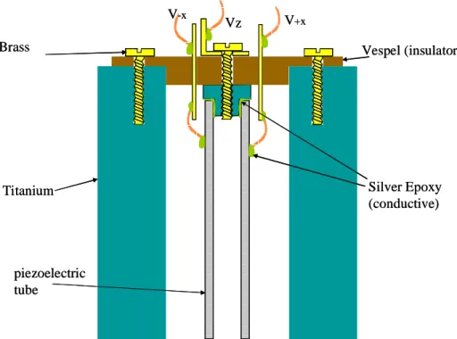
General descriptionFig. 2.1 CAD image of the microscope. Part n°2 in front, separated for clarity, is normally aligned to part n°3 by threaded rods (symbolized by dashed lines), and gently pressed against part n°1 by springs. Mating prismatic shapes are used to guide sliding parts (along the indicated X, Y and Z axes) which provide coarse positioning of the sensor tip above a fixed sample on three independent orthogonal axes. The sliding parts are actuated by inertial stick-slip motion of four shear-mode piezo stacks for each axis. Fine scanning of the sample surface is done by a vertical piezoelectric tube, which performs 3-D positioning. The sample is fixed and connected onto a sample holder, which plugs into a socket soldered onto a printed circuit board (PCB). The base is thermally anchored to the 30 mK plate of the inverted dilution fridge.