HAL Id: tel-01163511
https://tel.archives-ouvertes.fr/tel-01163511v2
Submitted on 19 Jan 2017HAL is a multi-disciplinary open access
archive for the deposit and dissemination of sci-entific research documents, whether they are
pub-L’archive ouverte pluridisciplinaire HAL, est destinée au dépôt et à la diffusion de documents scientifiques de niveau recherche, publiés ou non,
Emerging concepts in time-resolved quantum
nanoelectronics
Benoit Gaury
To cite this version:
Benoit Gaury. Emerging concepts in time-resolved quantum nanoelectronics. Physics [physics]. Uni-versité de Grenoble, 2014. English. �NNT : 2014GRENY026�. �tel-01163511v2�
THÈSE
Pour obtenir le grade de
DOCTEUR DE L’UNIVERSITÉ DE GRENOBLE
Spécialité : Physique théoriqueArrêté ministériel : 7 août 2006
Présentée par
Benoit GAURY
Thèse dirigée parXavier WAINTAL
préparée au sein INAC/SPSMS/GT
et del’Ecole Doctorale de Physique
Emerging
concepts
in
time-resolved quantum nanoelectronics
Thèse soutenue publiquement le14 octobre 2014,
devant le jury composé de :
M. Christopher BÄUERLE
Directeur de recherche CNRS, Institut Néel, Président
M. Anton AKHMEROV
Assistant Professor, Delft University of Technology, Rapporteur
M. Christian GLATTLI
Directeur de recherche, CEA-Saclay, Rapporteur
M. Pascal DEGIOVANNI
Directeur de recherche CNRS, Ecole Normale Supérieure de Lyon, Examinateur
M. Peter SAMUELSSON
Associate Professor, Lund University, Examinateur
M. Xavier WAINTAL
A B S T R A C T
With the recent technical progress, single electron sources have moved from theory to the lab. Conceptually new types of experiments where one probes directly the internal quantum dynamics of the devices are within grasp. In this thesis we develop the analytical and numerical tools for han-dling such situations. The simulations require appropriate spatial resolu-tion for the systems, and simulated times long enough so that one can probe their internal characteristic times. So far the standard theoretical approach used to treat such problems numerically—known as Keldysh or NEGF (Non Equilibrium Green’s Functions) formalism—has not been very successful mainly because of a prohibitive computational cost. We propose a refor-mulation of the NEGF technique in terms of the electronic wave functions of the system in an energy–time representation. The numerical algorithm we obtain scales now linearly with the simulated time and the volume of the system, and makes simulation of systems with 105−106 atoms/sites feasible. We leverage this tool to propose new intriguing effects and exper-iments. In particular we introduce the concept of dynamical modification of interference pattern of a quantum system. For instance, we show that when raising a DC voltage V on an electronic Mach-Zehnder interferom-eter, the transient current response oscillates as cos(eVt/¯h). We expect a wealth of new effects when nanoelectronic circuits are probed fast enough, and the tools and concepts developed in this work shall play a key role in the analysis and proposal of upcoming experiments.
A C K N O W L E D G M E N T S
I am very grateful to my supervisor, Xavier Waintal, for trusting me with this topic and for his guidance during these three years. Xavier, you have been a a great advisor. Thank you for teaching me your scientific rigor, for your ever lasting enthusiasm and good mood. You are incredibly good at motivating people and making them give their best. I will keep in mind your precious quotations and pass them to future generations.
I want to thank Christopher Bäuerle, Pascal Degiovanni, Perter Samuels-son, Christian Glattli and Anton Akhmerov for reading my work and being in my PhD defense committee.
A PhD thesis is also about the lab and the office mates. I started my PhD with Oleksii Shevtsov who helped me go through the Keldysh formalism and the Green’s functions. I will remember you as the guy for whom every-thing is “simple”. I also think of Caroline Richard and Driss Badiane for our conversations about physics. Not all the questions were answered but it was definitely good brainstorming. I also spent some good time with Vladimir Mariassin who taught me a few Russian words. I hope you will keep the chocolate breaks alive. Regarding this thesis work, I thank Matthieu Santin who participated on the propagation and spreading of a voltage pulse. I also thank Joseph Weston for his nice work on the numerical aspects. You did a good job Joseph, and lots of results I can present here are because of your efforts. I appreciated our conversations about physics and life with Vladimir, it was a lot of fun.
I also thank Christoph Groth, our computer guru, for his help in my various numerical implementations, and David Luc for making a nice 3D picture for the Fabry-Perot cavity. In the lab I also spent some time with Julia Meyer and Manuel Houzet, thank you for your advice in presenting my work.
Finally I thank my parents, Marie-Elise and Jacques, and my elder brother Matthieu for their presence and constant support from the beginning of it all.
C O N T E N T S
i g e n e r a l i n t r o d u c t i o n 1
1 i n t r o d u c t i o n (english) 3
1.1 Electronic interferometers in mesoscopic physics . . . 4
1.2 From AC to time-resolved quantum transport . . . 7
1.3 Outline of this thesis . . . 9
1.3.1 Chapter3: Various approaches to time-resolved
quan-tum transport . . . 9
1.3.2 Chapter4: Landauer formula for voltage pulses . . . . 11
1.3.3 Chapter5: Strategies for numerical simulations . . . . 11
1.3.4 Chapter6: Propagation and spreading of a charge pulse 12
1.3.5 Chapter 7: Dynamical control of interference using
voltage pulses in the quantum regime . . . 13
1.3.6 Chapter8: Numerical simulations of time-resolved
quan-tum transport in the quanquan-tum Hall effect regime . . . . 14
2 i n t r o d u c t i o n (français) 15
2.1 Interféromètres électroniques en physique mésoscopique . . . 16
2.2 Du transport quantique AC à résolu en temps . . . 20
2.3 Résumé des chapitres . . . 21
2.3.1 Chapitre3: Différentes approches du transport
quan-tique résolu en temps . . . 22
2.3.2 Chapitre4: Une formule de Landauer pour pulses de
tensions . . . 23
2.3.3 Chapitre5: Stratégies de simulations numériques . . . 24
2.3.4 Chapitre 6: Propagation et étalement d’un pulse de
charges . . . 24
2.3.5 Chapitre 7: Contrôle dynamique d’interférence
util-isant des pulses de tension dans le régime quantique . 25
2.3.6 Chapitre8: Simulations numériques du transport
tique résolu en temps dans le régime d’effet Hall quan-tique. . . 26
ii f o r m a l i s m a n d n u m e r i c a l a l g o r i t h m s f o r t i m e-dependent
q ua n t u m t r a n s p o r t 29
3 va r i o u s a p p r oa c h e s t o t i m e-resolved quantum
trans-p o r t 31
3.1 Theory and numerical simulations of time-resolved quantum transport . . . 31
3.2 Generic model for time-dependent mesoscopic devices . . . . 33
3.3 Keldysh formalism and non-equilibrium Green’s functions . . 34
3.3.1 Equations of motion for the Retarded (GR) and Lesser (G<) Green’s functions . . . 34
3.3.2 Equations of motion for the leads self-energies . . . 37
3.4 Wave-function (WF) approach . . . 38
3.4.1 Construction of the wave function . . . 38
3.4.2 Effective Schrödinger equation . . . 40
3.5 Time-dependent scattering theory . . . 42
3.5.1 Conducting modes in the leads . . . 42
3.5.2 Construction of the scattering states . . . 43
3.5.3 Connection to the wave function approach . . . 44
3.5.4 Generalization of the Fisher-Lee Formula . . . 44
3.5.5 Link with the partition-free initial condition approach 45 3.5.6 “Floquet wave function” and link with the Floquet scattering theory . . . 46
4 l a n d au e r f o r m u l a f o r v o lta g e p u l s e s 49 4.1 Total number of injected particles . . . 49
4.2 Scattering matrix of a voltage pulse . . . 50
4.3 Voltage pulses in multiterminal systems . . . 52
5 s t r at e g i e s f o r n u m e r i c a l s i m u l at i o n s 57 5.1 Non-equilibrium Green’s functions approach . . . 57
5.1.1 GF-A: brute-force integration of the NEGF equations . 58 5.1.2 GF-B: Integrating out the time-independent subparts of the device . . . 58
5.1.3 GF-C: integration scheme that preserves unitarity . . . 60
5.2 Numerical implementation of the wave function approach . . 61
5.2.1 WF-A: direct integration of Eq. (3.34) . . . 62
5.2.2 WF-B: subtracting the stationary solution . . . 62
5.2.3 WF-C: from integro-differential to differential equation 62 5.2.4 WF-D: faster convergence using the wide band limit . 63 5.3 Numerical tests of the different approaches . . . 65
5.3.1 Green’s function based algorithms . . . 65
5.3.2 Wave functions based algorithms . . . 66
5.3.3 Relative performance of the different approaches . . . 68
5.4 Integral over energies for the wave function approach . . . 69
5.5 A comment on the electrostatics . . . 71
iii n e w c o n c e p t s a n d e x p e r i m e n ta l p r o p o s a l s 75 6 p r o pa g at i o n a n d s p r e a d i n g o f a c h a r g e p u l s e 77 6.1 Scattering matrix of a one-dimensional chain in presence of a voltage pulse . . . 77
6.2 Spreading of a voltage pulse inside a one-dimensional wire: analytics . . . 80
6.3 Numerical calculations of the spreading of a voltage pulse inside a one dimensional wire . . . 82
6.4 Spreading of a charge pulse in the quantum Hall regime . . . 85
7 d y na m i c a l c o n t r o l o f i n t e r f e r e n c e i n m e s o s c o p i c d e -v i c e s 89 7.1 Model and DC characterization of the Fabry-Perot cavity . . . 90
7.2 Voltage pulses in the quantum regime . . . 92
7.3 Dynamical control of interference pattern . . . 95
7.3.1 Propagation of a phase domain wall . . . 95
7.3.2 Analytical calculation of the number of transmitted particles . . . 97
7.3.3 Interference visibility with temperature and pulse char-acteristics . . . 99
7.4 Towards experiments with the Mach-Zehnder interferometer 100
7.4.1 Simulation of an electronic Mach-Zehnder interferom-eter . . . 101
7.4.2 A comment on electron-electron interactions . . . 105
7.5 Generalization: the AC Josephson effect without supercon-ductivity . . . 106
8 n u m e r i c a l s i m u l at i o n s o f t i m e-resolved quantum trans-p o r t i n t h e q ua n t u m h a l l e f f e c t r e g i m e 111
8.1 Quantum Hall regime in discretized systems . . . 112
8.1.1 Magnetic field in numerical calculations . . . 112
8.1.2 DC settings for the quantum Hall effect regime . . . . 113
8.2 Additional settings for time-dependent numerics . . . 114
8.2.1 Filtering slow propagating modes . . . 114
8.2.2 Dealing with abrupt geometries . . . 115
8.3 Radio-frequency (RF) protocol for stopping voltage pulses . . 117
8.3.1 Mechanism for stopping single electron pulses . . . 117
8.3.2 Numerical results . . . 120
8.3.3 Mach-Zehnder analysis of the voltage pulse . . . 121
8.3.4 Effect of the disorder on the “stop and release” protocol123
8.3.5 A comment on charge relaxation . . . 124
iv g e n e r a l c o n c l u s i o n 127 9 c o n c l u s i o n (english) 129 10 c o n c l u s i o n (français) 131 v a p p e n d i x 135 a d y s o n e q uat i o n f o r t h e r e ta r d e d a n d l e s s e r g r e e n’s f u n c t i o n s 137 b va r i o u s a na ly t i c a l r e s u lt s f o r g r e e n’s functions of t h e 1 d c h a i n 139 b i b l i o g r a p h y 141 l i s t o f p u b l i c at i o n s 151 ix
1
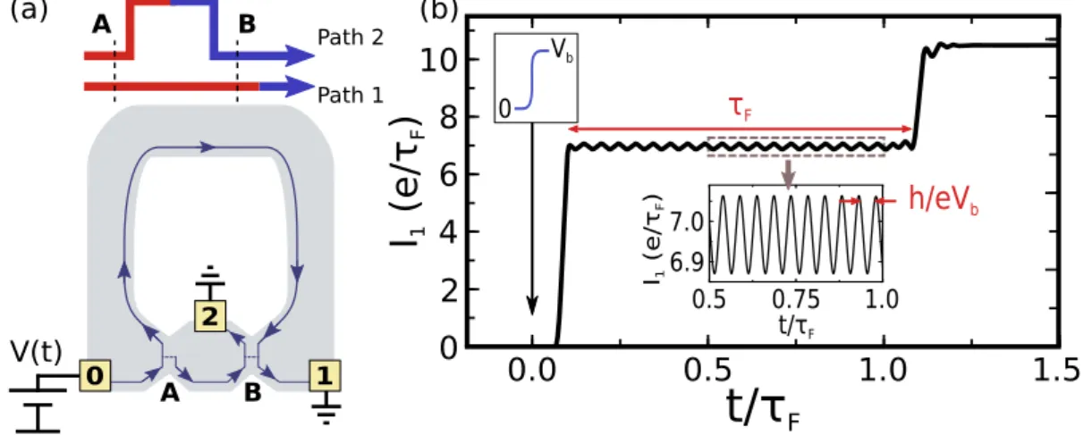
I N T R O D U C T I O N ( E N G L I S H )In this thesis we study the theory of low temperature nanoelectronic ex-periments in the GHz range and above. Keeping in mind that 1 K corre-sponds to 20 GHz, one finds that as the signals frequencies get higher, they become larger than the thermal background and eventually reach the in-ternal characteristic frequencies of the systems. Conceptually new types of experiments become possible where one probes directly the internal quan-tum dynamics of the devices. Let us start by discussing a simple example. The device is an electronic Mach-Zehnder interferometer, as sketched in Fig.1.1(a), implemented in a two-dimensional electron gas under high
mag-netic field (we will come back to it later). In the quantum Hall regime the bulk of the electronic gas is insulating and the electrons propagate only on the edges of the sample. Quantum point contacts (A and B) act as beam-splitters and make the system a two-path interferometer. The upper arm is much longer than the lower one, which implies an extra time of flight
τF = L/vg (with L the extra length of the upper arm with respect to the
lower one and vg the group velocity of the edge state). At t =0 one raises
the bias voltage applied on contact 0 and monitors the current I1(t) as a
function of time. The most noteworthy feature of Fig. 1.1(b) lies in the
transient regime; the current oscillates with frequency eVb/h around a DC
component (Vb final value of the DC bias). The reasoning leading to this
behavior is quite straightforward. As we raise the voltage bias, the wave function originated from contact 0 accumulates a phase difference eieVbt/¯h between its front and its rear. The device uses the delay time τF between
2 A B A B Path 2 Path 1 1 0 V(t) (a) (b)
I
1(
e/
τ
F)
0.0 0.5 1.0 1.5t/τ
F 0.5 0.75 1.0 I1 ( e/ τF ) t/τF τF 0 2 4 6 8 10 6.9 7.0 h/eVb 0 VbFigure 1.1 – (a) A 3 terminal Mach-Zehnder interferometer in the quantum Hall regime. The semi-transparent quantum point contacts A and B act as beamsplitters. Upper inset: schematics of the two interfering paths. (b) Transmitted current at contact 1.
the two arms to create an interference between the rear and the front of the wave function, generating the oscillatory behavior. Here we probed the time of flight of the interferometer by raising a DC potential faster than τF.
We will later call this effect dynamical control of interference pattern.
The objective of this work is twofold. On the one hand, we aim to develop the analytical and numerical tools for handling the example above. This re-quires to simulate devices with an appropriate spatial resolution (three ter-minals and magnetic field in that case), for times long enough so that one can probe the internal characteristic times of the systems (the delay time τF
in the example above). While there already exist standard approaches to investigate time-dependent quantum transport, the numerical implementa-tion has lacked of efficiency so far. On the other hand, the kind of effect presented above calls for new concepts as we have just shown. We shall provide along this thesis with new ways of thinking the quantum transport beyond the adiabatic limit.
This introduction is organized as follows. We start with an overview of the field of mesoscopic physics to which this work belongs in section 1.1,
with a particular emphasis on electronic interferometers. We will continue in section1.2with a review of the theoretical developments of AC and
time-resolved quantum transport, and we will finally summarize our work in section 1.3 with an outline of our results for each chapter.
1.1 e l e c t r o n i c i n t e r f e r o m e t e r s i n m e s o s c o p i c p h y s i c s
The domain of mesoscopic physics lies between particle physics and bulk physics. In the former, the characteristic size of a device is small enough for it to exhibit a quantum behavior while in the latter, it is large enough to present many-body features. The characteristic lengths limiting the scope of the mesoscopic domain are then the atomic scale (the angstrom) and the phase coherence length Lφ. This latter length represents the distance over
which the phase of the electronic wave function remains unchanged. Be-yond this length, all interference effects resulting from the wave-like nature of electrons are washed out, and their quantum behavior is lost [1, 2]. That
is why phase coherence can be considered as the hallmark of mesoscopic physics. The rise of the domain in the 90s is related to the increased ca-pability to reduce the dimensionality of the systems, which enhances the quantum interference effects. One defines the dimensionality of a system by comparing its characteristic size with the Fermi wave length λF [3]:
3D: λF Lx ∼Ly ∼ Lz
2D: Lx <λF Ly ∼ Lz
1D: Lx ∼ Ly <λF Lz
0D: Lx ∼ Ly ∼Lz <λF
In the early years, normal metals like gold were the usual material for ex-periments. However, the high carrier density of metals (of the order of
1022 cm−3) has two main drawbacks. First it makes the Fermi wave length very small (of the order of the angstrom), which renders a confinement of electrons difficult even in two dimensions. The second consequence is the impossibility to use gate voltages to vary this carrier density (this would cost a huge amount of electrostatic energy). In addition, the phase coher-ence length of metals is of the order of the micrometer only [4]. One bright
aspect of metals is that some of them become superconducting at low tem-perature (e.g. aluminium below 1.2 K) [5]. The superconducting phase
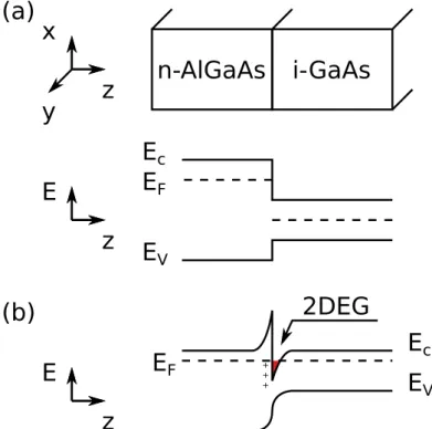
be-coming another “button” to play with. In the 1990s semiconductors started to be used. Their great advantage over metals is that one can control their lower carrier density (between 1014 cm−3and 1019 cm−3) by nearby metallic gates. It allows one to reduce the dimensionality of devices to 1D or even down to 0D to form quantum dots [6]. A typical example of such
semicon-ductor structure is the two-dimensional electron gas formed at the interface
E
cE
FE
V2DEG
E
VE
cE
Fn-AlGaAs i-GaAs
x
y
E
z
z
z
E
+ + +(a)
(b)
Figure 1.2 – Conduction and valence bands line-up in a heterojunction made of n-doped AlGaAs and intrinsic GaAs, (a) before and (b) after the charge transfer. Plus symbols are positively charged donors and the red area is the two-dimensional electron gas.
of the GaAs/AlGaAs heterostructure. The formation of this electron gas is described in Fig. 1.2. Before the line-up of energy levels, the Fermi
en-ergy in the n-doped AlGaAs layer is higher than in the intrinsic GaAs layer. Electrons therefore pour in GaAs from AlGaAs leaving positively charged donors behind (plus symbols in Fig.1.2(b). This creates an electric field that
bends the bands. At equilibrium the Fermi levels are aligned and a two-dimensional electron gas has formed at the GaAs/AlGaAs interface.
Although the phase of the electronic wave function is a central object for a mesoscopic physicist, one has to resort to interference processes to probe
it—as it cannot be measured directly. The effects of such processes are nat-urally present in mesoscopic systems—for instance in the universal conduc-tance fluctuations [7]—but can also be engineered with well defined
inter-ferometers. An important ingredient of mesoscopic experiments is the mag-netic field and the associated Aharonov-Bohm effect [8]. Unlike photons,
electrons are charged particles and couple to the vector potential A of the~ electromagnetic field even when the local magnetic field ~B is zero (realized when~B = ~∇ × ~A= ~0). As an electron propagates along an identified path p, its wave function acquires a phase given byRpd~r· (~k(~r) +eA~(~r)) with~k the wave vector. The first term comes from the geometrical path followed by the electron, and the second one arises from its coupling with the vector po-tential. In 1985 Webb et al. observed for the first time the oscillations of the magnetoresistance with the number of magnetic flux quanta (h/e) crossing through a gold ring [9] (see Fig. 1.3). While such a system might be called
a two-path interferometer, it suffers from the existence of multiple paths around the ring. One can remedy this spurious effect using, for instance, a flying qubit configuration [10]. Other types of interferometers derive from
setups usually found in optics. For example Fabry-Perot cavities (two re-flecting surfaces facing each other) are present in numerous devices. Such a resonator can be implemented using carbon nanotubes [11, 12], where
the Shottky barriers that form at the nanotube-contact interfaces act as the reflecting barriers (role played by the mirrors in optics). As one reduces the transparency of the “mirrors”, the modes of the cavity become true bound states of the system. Such a situation is very close to the Andreev bound states occurring in Josephson junctions [13]. Fabry-Perot cavities
also appear in semiconductor nanowires [14] in a similar way, or can be
en-(b) (a)
Figure 1.3 – (a) Magnetoresistance of a gold ring measured at T = 0.01 K. (b) Fourier power spectrum of the magnetoresistance containing peaks at h/e and h/(2e). Inset: photograph of the ring with inside diameter 784 nm and wire width of 41 nm [9].
gineered in a two-dimensional electron gas in the quantum Hall regime [15].
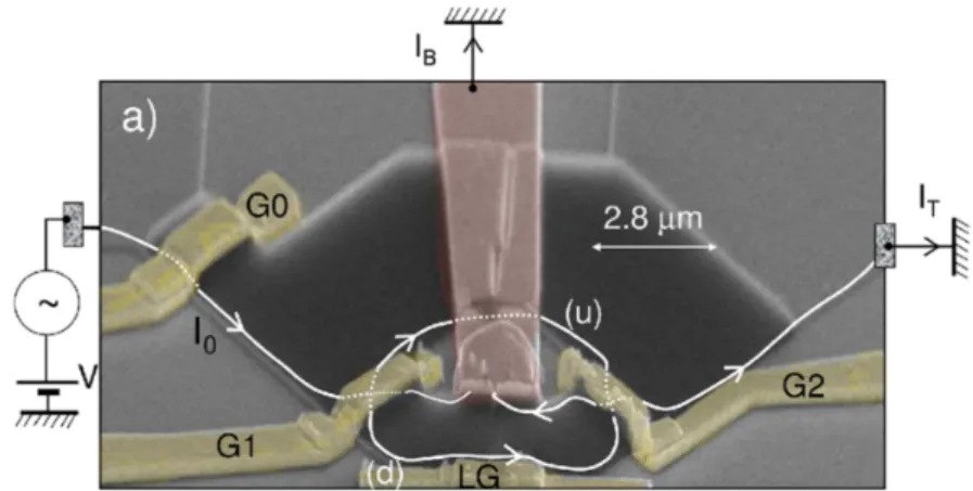
A more involved setup is the electronic analogue of the Mach-Zehnder in-terferometer [16, 17, 18]. Fig. 1.4 depicts the three-terminal device used
in [17], realizing a two-path interference between quantum Hall edge
chan-nels. These edge channels are separated and recombined by the quantum
Figure 1.4 – Scanning electron microscope view of Mach-Zehnder interferometer. G0, G1, and G2 are quantum point contacts acting as beamsplitters. The white lines represent the two interfering edge channels [17].
point contacts G1 and G2. A lateral gate (LG) can be used to modify the
length of the lower path. This interferometer is experimentally complex to realize (central contact, high magnetic field), but it is very simple from a theoretical point of view. Indeed, as shown by the white lines in Fig. 1.4
only two paths can interfere.
In this context we are interested in the physics of time-resolved quantum transport in low-dimensional devices. The term “time-resolved” means that the typical duration of the time-dependent perturbations can be considered finite. We present this domain in the next section.
1.2 f r o m a c t o t i m e-resolved quantum transport
The history of AC quantum transport probably starts in the 1960s with the prediction and measurement of the photon assisted tunneling [19]. Tien and
Gordon described the quantum transport in a two-terminal nanostructure subjected to both DC and AC voltages in a simple manner. They related the DC current in presence of an AC bias voltage with frequency ω to the I-V curves I(V)of this nanostructure in absence of AC voltage [20],
Idc(V) =
∑
npnI(V+n¯hω/e), (1.1)
where the coefficients pn depend on the amplitude and the shape of the
AC perturbation. This effect, also known as the Tien-Gordon effect, has attracted some renewed attention recently in the context of noise measure-ments [21]. A motivation for such experiments lies in the possibility given
(¯hω > kBT), allowing for the observation of the effects of quantum
fluc-tuations on the mesoscopic apparatus (circuits amplifiers, detectors) [22].
Around the same time was the discovery of the AC Josephson effect [23,24].
On applying a DC voltage bias V on a superconducting junction, one ob-tains an AC current oscillating at the frequency 2eV/h. Other early exper-iments showed that it was possible to generate a DC current with the help of an AC perturbation in the absence of DC bias, which is called pump-ing [25, 26]. The AC perturbation can be radio-frequency voltages applied
to gates using the Coulomb blockade effect [27] or, the modulation of the
phase of the order parameter of superconducting electrodes using the afore-mentioned AC Josephson effect [28]. More recent experiments include the
measurement of a quantum LC circuit [29], the statistics of the photons
emitted by a tunnel junction [30, 31] and the minimization of the shot noise
using multiple harmonics [32].
An important point that was recognized early by Büttiker and his collabo-rators is that a proper treatment of the electrostatics of a nanostructure was crucial when dealing with finite frequency quantum transport [33,34,35,36, 37]. Solving naively the time-dependent Schrödinger equation
incorporat-ing the AC perturbation does not suffice to compute the correct AC current response. At finite frequency two main issues arise. On the one hand, in the non-interacting AC theory the electronic density fluctuates with space and time. As a result the current is no longer a conserved quantity. On the other hand, the particle current response (not identical to the electrical current anymore as it is in DC) depends on the voltage distribution across the nanostructure. Both problems are dealt with using nearby gates capaci-tively coupled to the conductors that screen the extra charges accumulated in the system. This restores the neutrality of the global system, as well as current conservation once the displacement currents (currents flowing through the plates of the capacitors) are properly included. One then finds that it is difficult to observe the internal time scales of a device as they are often smaller than the classical RC time of the above capacitors. The theory of AC quantum transport has now evolved into a field in itself which is not the focus of this work. We refer to [38] for an introduction to the (Floquet)
scattering theory and to [39] for the numerical aspects.
Time-resolved quantum transport is not, a priori, very different from AC quantum transport. A series of seminal works on time-resolved quantum electronics showed however that the current noise associated with voltage pulses crucially depends on their actual shape (i.e. on the details of the har-monics content and of the relative phases of the various harhar-monics) [40,41].
More precisely, Levitov and collaborators found that pulses of Lorentzian shape can be noiseless while other shapes are associated with extra electron-holes excitations that increase the noise of the signal. These predictions are the object of an intensive experimental activity [42, 43]. Meanwhile,
other experiments are looking for various ways to construct coherent sin-gle electron sources and reproduce known quantum optics experiments with electrons. This rising field is sometimes referred to as “electronic
quantum optics”. Ref. [44] used a small quantum dot to make such a
source [45, 46, 47, 48] which was later used in a Hanbury-Brown and Twiss
setup [49], and in [50] to perform an electronic Hong-Ou-Mandel
experi-ment. A similar source, yet working at much larger energy has been re-cently demonstrated in [51]. Another route used surface acoustic waves to
generate a propagating confining potential that transports single electrons through the sample [52, 53]. These experiments are mostly performed in
the two-dimensional gases heterostructures introduced earlier taking ad-vantage of the small velocities (estimated around 104−105 m.s−1 in the quantum Hall regime) and large sizes (usually several µm) to work in the GHz range. Smaller devices, such as carbon nanotubes, require the use of frequencies in the THz range. Although THz frequencies are still experi-mentally challenging, detection schemes in these range have been reported recently [54]. Progress in cryogenic technology makes it possible to access
the high frequencies that are necessary to probe the internal time scale of nanoelectronic devices. The motivation for such work relate to the con-trol over the orbital and spin degrees of freedom of single electrons in the wider picture of quantum computation [55], quantum information
process-ing [56, 57], and quantum teleportation [58, 59].
1.3 o u t l i n e o f t h i s t h e s i s
In this thesis we reformulate the standard approach to time-dependent transport with a wave function in an energy–time representation. This work allows us to simulate systems containing more than 105 sites during 106 time steps going beyond the adiabatic limit and optics physics. In addition we propose new concepts and experiments. We showed the dynamical con-trol of interference at the beginning of this introduction and we propose ways to observe it experimentally; we also propose to stop and release an electron of a charge pulse in the quantum Hall regime. Here we review the present research results accessible in each chapter.
1.3.1 Chapter3: Various approaches to time-resolved quantum transport
Chapter 3 contains the theory of time-dependent transport developed in
this thesis work. We consider a generic system made of several semi-infinite electrodes and a central region as sketched in Fig. 1.5. The tight-binding
Hamiltonian for such a system reads ˆ
H(t) =
∑
i,jHij(t)c†icj, (1.2)
where c†i (cj) are the Fermionic creation (annihilation) operators of a
one-particle state on site i. The basic objects of the Keldysh or NEGF formalism are the Retarded (GR) and Lesser (G<) Green’s functions defined in the central region ¯0. Integrating out the degrees of freedom of the leads into
Figure 1.5 – Sketch of a generic multiterminal system where the central part ¯0 (blue circles) is connected to three semi-infinite leads ¯1, ¯2, ¯3 (yellow circles). The leads are kept at equilibrium with temperature Tm¯ and chemical potential µm¯.
self-energy terms, one obtains effective equations of motion for GR and G< [60, 61], i∂tGR(t, t0) =H¯0¯0(t)GR(t, t0) + Z du ΣR(t, u)GR(u, t0) (1.3) G<(t, t0) = Z du Z dv GR(t, u)Σ<(u, v)[GR(t0, v)]† (1.4) Introducing the wave function ΨαE(~r, t)which depends on space~r and time
t as well as on the injection energy E and mode α, we find that it obeys a Schrödinger equation with an additional source term,
i¯h∂ ∂tΨαE(~r, t) =H¯0¯0(t)ΨαE(~r, t) + Z duΣR(t−u)ΨαE(u) +√vαξαE(~r)e −iEt/¯h, (1.5) where ξαE(~r) corresponds to the transverse wave function of the
conduct-ing channel α at the electrode–device interface (the number α is labelconduct-ing both the different channels and the electrodes to which they are associated) and vα is the associated mode velocity. The Lesser Green’s function, hence
the physical observables (density, current, ...), are then simply expressed in terms of these wave functions,
G<(t, t0) =
∑
α
Z dE
2π i fα(E)ΨαE(t)ΨαE(t
0)†, (1.6)
where fα(E) is the Fermi function in the electrode of channel α. The source
term and mode velocities in Eq. (1.5) are standard objects of the theory of
stationary quantum transport and are readily obtained, while Eq. (1.5) itself
can (and will) be integrated numerically.
In addition to the reformulation of the NEGF technique, we draw explicit connections with two other approaches to time-dependent transport. We first show the equivalence of our wave function method with the scattering approach. By constructing the scattering states we find that they coincide
with the wave function ΨαE(t) inside the central region of the system. A
second connection is drawn with the partition-free approach mentioned in the previous section. We show that our wave function and the one obtained within the partition-free approach are the same.
1.3.2 Chapter4: Landauer formula for voltage pulses
Chapter4is devoted to the derivation of a generalization of the Landauer
formula to voltage pulses in multiterminal systems. We find that the num-ber of particles is a relevant quantity for time-resolved quantum transport. Indeed we show that it is conserved and gauge invariant. We first assume a system at thermal equilibrium without net current flowing; and also that the electrons do not experience any reflection at the location of the voltage pulse. We thus find that on applying a voltage pulse Vm¯ on lead ¯m, the
number of particles received in lead ¯p reads, n¯p =
∑
¯ m N¯p ¯m N¯p ¯m =∑
β∈¯pα∑
∈m¯ Z de 2π|S 0 ¯pβ, ¯mα(e)|2 Z dE 2π|Km¯(E−e)| 2[ f(E) − f(e)], (1.7) where S0¯pβ, ¯mα(e) is the DC scattering matrix of the system in the absence ofa voltage pulse, and Km¯(E) is the harmonic content of the pulse applied on
lead ¯m, Km¯(E) = Z dt eiφm¯(t)+iEt, (1.8) with φm¯(t) = Rt −∞du Vm¯(u).
1.3.3 Chapter5: Strategies for numerical simulations
Chapter 5 deals with the numerical aspects of the NEGF and wave
func-tion (WF) approaches discussed in chapter3. We propose several schemes
(three for NEGF and four for the wave function) illustrated with the propa-gation of a voltage pulse along a one-dimensional chain. The relative com-parison of the relevant implementations is given in Table 1.1. We denote
N the total number of sites of the central region and S the number of sites connected to the electrodes. WF-D is our best algorithm and is the one used in the rest of this work. While the numerical resolution of Eq. (1.5) is done
without difficulty, the integration over energy is often a source of compli-cation. In particular, we show that contributions with vanishing velocity make it difficult to obtain particle conservation. We show that one recov-ers particle conservation when integrating over a long time. We propose to filter these contributions of low energy to recover a Fermi level physics expected in the long-time limit. Finally we discuss our choice of boundary
Algorithm CPU (1D) Estimated CPU (2D) Scaling of CPU WF-D 1 104 (t/ht)NE[N+γtS]
WF-B 40 4.107 (t/ht)NE[N+ (t/ht)S2]
GF-C 104 1012 (t/ht)2S3 (*) GF-A 105 1014 (t/ht)2S2N (*)
Table 1.1 – Computation time in seconds for a calculation performed on a single computing core. 1D case: 20 sites (for GF-A the calculation has been done in parallel using 48 cores in order to obtain the results within a few hours). 2D case: 100×100 sites. The CPU time is estimated from the scaling laws except for WF-D where calculations of similar sizes could be performed. Third column: typical scaling of the computing time. A notable additional difference between the WF and GF methods is that the GF methods (*) only provide the observables at one given time per calculation while the WF methods give the full curve in one run. The typical number of energy points NE is 100 in this example.
conditions in the electrodes and we justify our model of an abrupt voltage drop used in this work.
1.3.4 Chapter6: Propagation and spreading of a charge pulse
We study in chapter 6 the propagation and spreading of a charge pulse
created by a voltage pulse applied to an Ohmic contact. We begin with a scattering approach for a one-dimensional chain, and continue in the continuous limit to find that charge density and current oscillations follow the spreading of the charge pulse. We show that these oscillations spread diffusively. We perform additional numerical simulations using the one-dimensional edge states of the quantum Hall regime as shown in Fig. 1.6.
Specifically we show that the spreading of the envelope of the charge den-sity∆X(t)spreads linearly in time. More precisely we identify two
contribu-t (ps) 75 120 165 0 2.5 5 -2.5 -5 x - vt (μm) x y
Figure 1.6 – Carte de la densité de charge liée à l’étalement d’un pulse de charge créé par un pulse de tension Lorentzien, V(t) =Vp/(1+ (t/τp)2), avec amplitude Vp =0.5i mV et durée τp =5 ps.
tions to the spreading. On the one hand, the calculations in the continuous limit gives, ∆X qu = t m∗∆X0 , (1.9)
with∆X0the initial spatial extension of the pulse, and m∗ the electron
effec-tive mass. On the other hand, a more classical picture based on a “hydro-dynamic” reasoning leads to
∆X cl = ¯nt m∗∆X 0 , (1.10)
where ¯n is the number of particles injected by the voltage pulse. The trans-port properties of a voltage pulse applied to an Ohmic contact are then related to its quantum nature that is bounded by ¯n≈1.
1.3.5 Chapter 7: Dynamical control of interference using voltage pulses in the quantum regime
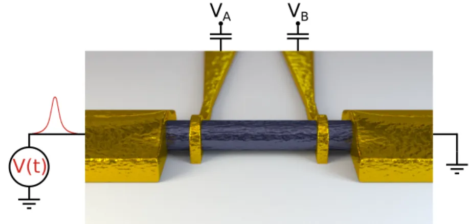
We start to study the time-dependent transport beyond the adiabatic limit in chapter 7. To this end we first consider a Fabry-Perot cavity as it is the
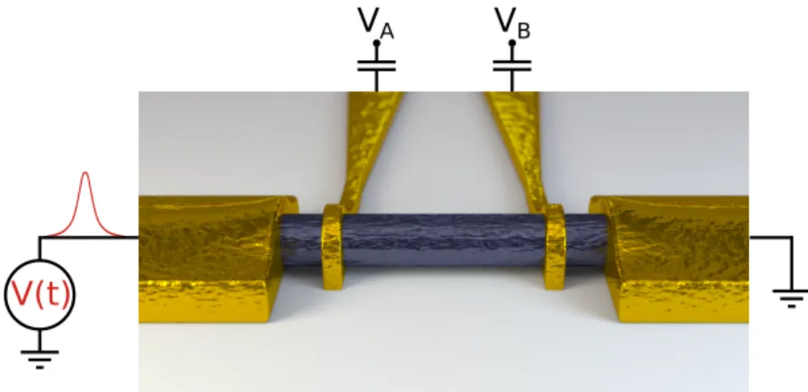
simplest system to exhibit a characteristic time scale (the time of flight inside the cavity). Such a cavity is made out of a quantum wire and two barriers as sketched in Fig.1.7. We find that on applying voltage pulses faster than the
VA VB
V(t)
Figure 1.7 – Schematic of our setup, a quantum wire connected to two electrodes. Two barriers A and B separated by a distance L are placed along the wire and a Gaussian voltage pulse V(t) is sent from the left. The barriers are characterized by the barrier heights (VAand VB).
time of flight of the cavity, we can dynamically control the relative phases of the paths taken by the electrons. This regime of fast pulses allows for the restoration of the interferences in presence of large bias voltages, neg-ative currents with respect to the direction of propagation of the voltage pulse, oscillations of the total transmitted charge with the total number of injected electrons. All our numerical findings are supported by analytical
derivations based on the formalism for voltage pulses developed in chap-ter4. We also validate our analysis further with the full scale simulation of
an electronic Mach-Zehnder interferometer in the quantum Hall regime. We generalize the concept of dynamical control of interference to the case of raising a DC bias voltage in the interferometers discussed above. We show that on applying a DC voltage Vb to an electronic interferometer, there
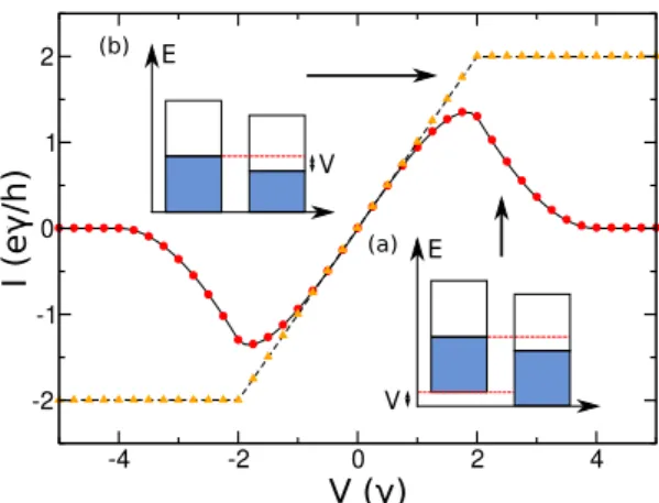
exists a universal transient regime where the current oscillates at frequency eVb/h. This effect is analogous to the AC Josephson effect.
1.3.6 Chapter 8: Numerical simulations of time-resolved quantum transport in the quantum Hall effect regime
In chapter 8 we first present the procedure that should be followed to
perform numerical simulations in the quantum Hall regime, and continue with the requirements specific to time-dependent transport. In particular we come back to the integration over energy necessary to compute observ-ables (see Eq. (1.6)). We find that the filtering potential engineered in
chap-ter5needs to be adapted to the peculiar density of states of a system in the
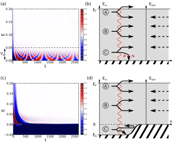
quantum Hall regime. In the last section of the chapter we discuss the in-terplay between the modification of the path followed by the electrons and the quantum dynamics of the electronic flow in a quantum circuit. Specif-ically, we study the propagation of charge pulses through the edge states of a two-dimensional electron gas in the quantum Hall regime. By sending radio-frequency (RF) excitations on a top gate capacitively coupled to the electron gas, we manipulate these edge states dynamically. We find that a fast RF change of the gate voltage can stop the propagation of the charge pulse inside the sample. This effect is intimately linked to the vanishing ve-locity of bulk states in the quantum Hall regime and the peculiar connection between momentum and transverse confinement of Landau levels. We pro-pose new possibilities for stopping, releasing and switching the trajectory of charge pulses in quantum Hall systems.
2
I N T R O D U C T I O N ( F R A N Ç A I S )Nous étudions dans cette thèse les expériences de nanoélectronique à basse température dans la gamme de fréquences du GHz et au-delà. En ayant à l’esprit que 1 K correspond à 20 GHz, on comprend que plus les fréquences des signaux s’accroissent, plus elles surpassent le bruit ther-mique, et finalement atteignent les fréquences caractéristiques des systèmes. Des expériences conceptuellment nouvelles deviennent possibles, où l’on sonde directement la dynamique quantique interne des systèmes. Com-mençons par discuter d’un exemple simple. Le système est un interféromètre électronique de Mach-Zehnder, comme schématisé en Fig. 2.1(a), réalisé
dans un gaz bi-dimensionnel d’électrons sous fort champ magnétique (nous y reviendrons plus tard). Dans le régime d’effet Hall quantique l’intérieur du gaz d’électrons est isolant et les électrons se propagent uniquement sur les bords du système. Les points de contact quantique (A et B) jouent le rôle de lame semi-réfléchissante et font de ce système un interféromètre à deux chemins. Le bras supérieur est beaucoup plus long que le bras inférieur, ce qui implique un temps de vol additionnel τF = L/vg (avec L la longueur
supplémentaire du bras supérieur par rapport au bras inférieur, et vg la
vitesse de groupe de l’état de bord). À t=0 on monte la tension appliquée au contact 0 et on enregistre le courant I1(t)en fonction du temps. Le point
notoire de la figure Fig.1.1(b) réside dans le régime transitoire. Le courant
oscille à la fréquence eVb/h autour d’une composante DC (Vb valeur finale
de la tension DC). Le rasionnement menant à ce comportement est plutôt direct. Lorsque l’on monte la tension, la fonction d’onde du contact 0
accu-2 A B A B Path 2 Path 1 1 0 V(t) (a) (b)
I
1(
e/
τ
F)
0.0 0.5 1.0 1.5t/τ
F 0.5 0.75 1.0 I1 ( e/ τF ) t/τF τF 0 2 4 6 8 10 6.9 7.0 h/eVb 0 VbFigure 2.1 – (a) Un interféromètre Mach-Zehnder à 3 terminaux dans le régime d’effet Hall quantique. Les points de contacts quantiques A et B jouent le rôle de miroir semi-réfléchissant. Insert: schéma des deux chemins qui interfèrent. (b) Courant transmis au contact 1.
mule une différence de phase eieVbt/¯h entre l’avant et l’arrière. Le système utilise le retard τF entre les deux bras pour créer une interférence, générant
le comportement oscillant. Ce que l’on a fait ici consiste à sonder le temps de vol de l’interféromètre en montant une tension DC plus vite que τF. Plus
tard, nous appellerons cet effet modification dynamique du motif d’interférence. L’objectif de ce travail de thèse est double. D’une part, nous développons les outils analytiques et numériques pour traiter l’exemple ci-dessus. Cela requiert de simuler des systèmes dont la résolution spatiale est appropriée (trois contacts et du champ magnétique dans ce cas), pendant des temps suffisamment longs pour sonder les temps caractéristiques des systèmes (ici le temps de vol τF). Alors qu’il existe déjà des méthodes standards
pour étudier le transport quantique dépendent du temps, l’implémentation numérique a manqué d’efficacité jusqu’à maintenant. D’autre part, le genre d’effet présenté avec notre exemple fait appel à de nouveaux concepts. Tout au long des pages qui suivent, nous allons donner de nouvelles façons de penser le transport quantique au-delà de la limite adiabatique.
Cette introduction est organisée comme suit. Nous commençons par une vue d’ensemble de la physique mésoscopique, à laquelle ce travail appar-tient, en section2.1, où l’on portera l’accent sur les interféromètres
électron-iques. Nous poursuivons en section2.2avec une revue des développements
théoriques du transport quantique AC et résolu en temps, et nous finirons par un résumé des chapitres en section2.3.
2.1 i n t e r f é r o m è t r e s é l e c t r o n i q u e s e n p h y s i q u e m é s o s c o p i q u e Le domaine de la physique mésoscopique se situe entre la physique des particules et la physique des systèmes massifs. Dans le premier cas, la taille caractéristique d’un système est suffisamment petite pour exhiber un com-portement quantique. Dans le second cas, le système est suffisamment large pour avoir les caractéristiques d’un comportement à N corps. Les tailles caractéristiques délimitant le cadre de la physique mésoscopique sont donc l’échelle atomique (l’angstrom) et la longueur de cohérence de phase Lφ.
Cette dernière longueur représente la distance sur laquelle la phase d’une fonction d’onde électronique reste inchangée. Au-delà de cette longueur, tous les effets résultant de la nature ondulatoire des électrons disparaissent et leur comportement quantique est perdu [1,2]. C’est pourquoi la longueur
de cohérence de phase peut être considérée comme la marque principale de la physique mésoscopique. L’essor de ce domaine dans les années 90 est lié à la capacité croissante de réduire la dimensionnalité des systèmes, ce qui renforce les effets quantiques. On définit la dimensionnalité d’un sys-tème en comparant ses dimensions caractéristiques à la longueur d’onde de Fermi λF [3]:
3D: λF Lx ∼Ly ∼Lz
2D: Lx <λF Ly ∼Lz
1D: Lx ∼Ly <λF Lz
0D: Lx ∼Ly ∼ Lz <λF
Dans les premières années de la physique mésoscopique, des métaux or-dinaires comme l’or étaient utilisés pour les expériences. Cependant, la haute densité de porteurs de charge des métaux (de l’ordre de 1022 cm−3) a deux inconvénients majeurs. D’abord cela implique une longueur d’onde de Fermi très petite (de l’ordre de l’angstrom), ce qui rend difficile le con-finement des électrons même en deux dimensions. Le second désavantage est qu’il est impossible d’utiliser des tensions de grille pour faire varier cette densité (cela coûterait une énergie électrostatique considérable). De plus la longueur de cohérence de phase dans les métaux est seulement de l’ordre du micromètre [4]. Un aspect intéressant émerge cependant en ce
que certains métaux sont supraconducteurs à basse température (par exem-ple l’aluminium en-dessous de 1.2 K) [5]. La phase du supraconducteur
est alors un nouveau bouton avec lequel on peut jouer. Dans les années 90 on a commencé à utiliser des structures à base de semiconducteurs. Le grand avantage des semiconducteurs sur les métaux est leur plus faible densité de porteurs de charge (entre 1014 cm−3 et 1019 cm−3) que l’on peut contrôler par des grilles métalliques. Ceci permet de résuire la
di-E
cE
FE
V2DEG
E
VE
cE
Fn-AlGaAs i-GaAs
x
y
E
z
z
z
E
+ + +(a)
(b)
Figure 2.2 – Alignement des bandes de conduction et de valence dans une hétéro-jonction formée de AlGaAs dopé n et de GaAs intrinsèque, (a) avant et (bC après le transfert de charges. Les symboles “plus” indiquent les donneurs ionisés, et la zone rouge est le gaz bi-dimensionnel d’électrons.
mensionnalité des systèmes à 1D ou même jusqu’à 0D pour former des boîtes quantiques [6]. Un exemple typique de telles structures
semicon-ductrices est le gaz bi-dimensionnel d’électrons qui se forme à l’interface de l’hétérostructure GaAs/AlGaAs. La formation de ce gaz d’électrons est décrite en Fig. 2.2. Avant l’alignement des niveaux d’énergie, l’énergie de
Fermi dans la couche d’AlGaAs dopé n est plus haute que celle de la couche de GaAs intrinsèque. En conséquence, les électrons se déversent dans GaAs à partir de AlGaAs, laissant derrière eux les donneurs ionisés (symboles plus dans Fig.2.2(b)). Ce phénomène crée un champ électrique qui plie les
bandes. À l’équilibre les niveaux de Fermi sont alignés et un gaz d’électrons bi-dimensionnel se trouve à l’interface GaAs/AlGaAs.
Bien que la phase de la fonction d’onde électronique soit un objet central pour le physicien mésoscopiste, on ne peut pas la mesurer directement et l’on doit recourir à des processus d’interférence pour la sonder. Les effets de tels processus sont naturellement présents dans les systèmes étudiés—on peut penser par exemple aux fluctuations universelles de conductances [7]—
mais peuvent aussi être construits par des interféromètres bien définis. Un ingrédient important des expériences est le champ magnétique et l’effet Aharonov-Bohm associé [8]. Contrairement aux photons, les électrons sont
des particules chargées et se couplent au potentiel vecteur A du champ élec-~ tromagnétique, même lorsque le champ magnétique local~B est nul (réalisé quand~B= ~∇ × ~A = ~0). Lorsqu’un électron se propage suivant un chemin p, sa fonction d’onde aquiert une phase donnée parRpd~r· (~k(~r) +eA~(~r))avec~k le vecteur d’onde. Le premier terme vient du chemin géométrique parcouru par l’électron, et le second provient du couplage avec le potentiel vecteur. En 1985 Webb et al. ont observé pour la première fois les oscillations de
(b) (a)
Figure 2.3 – (a) Magnétorésistance d’un anneau d’or mesurée à T = 0.01 K. (b) Densité spectrale de puissance de la magnétorésistance contenant des pics à h/e et h/(2e). Insert: photographie de l’anneau dont le diamètre interne est 784 nm la largeur du fil est 41 nm [9].
magnétorésistance avec le nombre de quanta de flux (h/e) traversant un an-neau d’or [9] (voir Fig.2.3). Alors qu’un tel système pourrait être vu comme
un interféromètre à deux chemins, l’existence de multiples chemins autour de l’anneau complexifie la situation. Ce problème peut être résolu en util-isant, par exemple, une configuration de qubit volant [10]. D’autres types
d’interféromètres proviennent de montages que l’on trouve usuellement en optique. Par exemple, les cavités Fabry-Perot (deux surfaces réfléchissantes face-à-face) sont présentes dans de nombreux systèmes. De tels résonateurs peuvent être créés en utilisant des nanotubes de carbone [11, 12], où les
barrières Shottky se formant à l’interface nanotube–contact jouent le rôle de barrières réfléchissantes (les miroirs en optique). Lorsqu’on réduit la trans-parence des “miroirs”, les modes de la cavité deviennent de véritables états liés. Une telle situation est alors très proche des états liés d’Andreev qui apparaissent dans les jonctions Josephson [13]. Les cavités Fabry-Perot sont
aussi présentes dans les nanofils semiconducteurs [14] de façon similaire,
mais peuvent aussi être créées dans un gaz bi-dimensionnel d’électrons en régime d’effet Hall quantique [15]. Un système un peu plus complexe est
l’analogue électronique de l’interféromètre de Mach-Zehnder (vu rapide-ment au début de cette introduction) [16, 17, 18]. La Fig. 2.4 montre le
système à trois terminaux utilisé dans [17], réalisant une interférence entre
deux canaux de bord de l’effet Hall. Ces canaux de bord sont séparés puis
Figure 2.4 – Vue au microscope électronique à balayage d’un interféromètre de Mach-Zehnder. G0, G1, et G2 sont les points de contact quantiques jouant le rôle de lame séparatrice. Les lignes blanches représentent les canaux de bord qui interfèrent [17].
recombinés par les deux points de contact quantique G1 et G2. Une grille
latérale (LG) permet de modifier la longueur du chemin inférieur. Cet in-terféromètre expérimentalement complexe à réaliser (le contact central est complexe à obtenir, un fort champ magnétique est nécessaire), est cepen-dant très simple du point de vu théorique. En effet il n’y a vraiment que deux chemins qui interfèrent , comme le montrent les lignes blanches en Fig.2.4.
Dans ce contexte nous nous intéressons à la physique du transport ré-solu en temps dans les structures à basses dimensions. Le terme “réré-solu
en temps” signifie que l’extension temporelle des perturbations peut être considérée comme finie. Nous présentons ce domaine dans la prochaine section.
2.2 d u t r a n s p o r t q ua n t i q u e a c à r é s o l u e n t e m p s
L’histoire du transport quantique AC commence probablement dans les années 1960 avec la prédiction et la mesure de l’effet tunnel photo-assisté [19].
Tien et Gordon ont décrit le transport quantique dans des nanostructures à deux terminaux soumises à des tensions DC et AC d’une façon simple. Ils ont relié le courant DC en présence d’une tension AC à la fréquence ω aux courbes I-V de la nanostructure en l’absence de tension AC [20],
Idc(V) =
∑
npnI(V+n¯hω/e), (2.1)
où les coefficients pn dépendent de l’amplitude et de la forme de la
perturba-tion AC. Cet effet, aussi connu sous le nom d’effet Tien-Gordon, a attiré de nouveau l’attention récemment dans le contexte des mesures de bruit [21].
Une motivation pour de telles expériences réside dans la possibilité que l’on a aujourd’hui de travailler à des fréquences dépassant le bruit ther-mique (¯hω >kBT). Cela permet d’observer les effets des fluctuations
quan-tiques sur l’appareillage de mesure (amplificateurs, détecteurs) [22]. Au
même moment l’effet Josephson AC était découvert [23, 24]. L’application
d’une tension continue V sur une jonction supraconductrice fournit un courant oscillant à la fréquence 2eV/h. D’autres expériences ont montré que l’on pouvait générer un courant DC par le biais d’une tension AC en l’absence de tension continue. On apelle cela le pompage [25, 26]. La
ten-sion AC peut être un signal radio-fréquence appliqué sur des grilles en utilisant le blocage de Coulomb [27] ou bien, la modulation de la phase du
paramètre d’ordre d’électrodes supraconductrices en usant de l’effet Joseph-son AC [28]. Plus récemment des expériences ont été réalisées sur un
cir-cuit LC quantique [29], sur la statistique des photons émis par une jonction
tunnel [30, 31] et sur la minimisation du bruit de grenaille en mélengeant
plusieurs harmonique [32].
Büttiker et ses collaborateurs ont remarqué très tôt qu’un bon traitement de l’électrostatique d’une nanostructure était crucial dans l’étude du trans-port quantique à fréquence finie [33, 34, 35, 36, 37]. Résoudre naivement
l’équation de Schrödinger dépendente du temps en incorporant une pertur-bation AC ne suffit pas pour calculer la réponse en courant d’un système. À fréquence finie, deux difficultés principales surgissent. D’une part, dans la théorie AC sans interaction la densité électronique fluctue dans l’espace et le temps. Il en résulte que le courant n’est plus une grandeur conservée. D’autre part, le courant de particule (maintenant différent du courant élec-trique contrairement au cas DC) dépend de la distribution de la tension à travers la nanostructure. Ces deux problèmes ont été résolus en considérant que des grilles couplées capacitivement au système permettent d’écranter
la charge qui s’y est accumulée. Ceci permet de restaurer la neutralité glob-ale du système, ainsi que la conservation du courant une fois que l’on a pris en compte les courants de déplacement (courants circulant à travers les grilles). On remarque alors qu’il est difficile d’observer les échelles de temps caractéristiques d’un système parce qu’elles sont souvent plus petites que le temps RC classique des capacités mentionnées. La théorie du trans-port quantique AC a évolué pour devenir un domaine bien défini. Nous reportons le lecteur à [38] pour une introduction à la théorie de la
diffu-sion (Floquet), et à [39] pour les aspects numériques. Ce domaine n’est
cependant pas l’objet de ce travail comme nous allons le voir maintenant. Le transport quantique résolu en temps n’est, a priori, pas très différent du transport quantique AC. Cependant, une série de travaux fondateurs por-tant sur l’électronique résolue en temps a montré que le bruit en courant associé à des pulses de tension dépend précisément de leur forme (c’est-à-dire de leur contenu en harmoniques et des phases entre celles-ci) [40, 41].
Plus précisément, Levitov et ses collaborateurs ont trouvé que des pulses de forme Lorentzienne peuvent être non bruités, alors que d’autres formes im-pliquent l’excitation de paires électron–trou qui augmentent le bruit du sig-nal. Ces prédictions font l’objet d’une intense activité expérimentale [42,43].
Pendant ce temps, d’autres expériences cherchent des moyens de construire des sources d’électrons uniques cohérents et reproduisent, avec des élec-trons, des expériences connues d’optique quantique. Ce domaine naissant est parfois dénommé “optique électronique quantique”. Ref. [44] utilise une
boîte quantique pour réaliser une telle source [45, 46, 47, 48] qui sera plus
tard utilisée dans un montage Hanbury-Brown and Twiss [49], ainsi que
dans [50] pour faire une expérience de Hong-Ou-Mandel. Une source
simi-laire, mais fonctionnant à plus grande énergie, a récemment été réalisée [51].
Une autre voie prise dans [52, 53] consiste à utiliser des ondes acoustiques
de surface pour générer un potentiel de confinement permettant de trans-port les électrons uniques à travers l’échantillon. Ces expériences sont prin-cipalement réalisées dans les gaz bi-dimensionnels d’électrons présentés plus tôt. La motivation pour de tels travaux repose principalement sur le fait que le contrôle des degrés de liberté de l’électron (spin et orbital) est au coeur des problématiques de calcul quantique [55], d’information
quantique [56, 57] et de téléportation [58, 59].
2.3 r é s u m é d e s c h a p i t r e s
Dans cette thèse, on reformule l’approche standard du transport dépen-dent du temps à l’aide d’une fonction d’onde dans une représentation énergie–temps. Ce travail nous permet de simuler des systèmes contenant 105 sites durant 106 pas de temps. On peut alors aller au-delà de la lim-ite adiabatique et de l’optique. Nous proposons aussi de nouveaux con-cepts. On a déjà évoqué le contrôle dynamique du motif d’interférence en introduction, on donne aussi des moyens de l’obsever expérimentale-ment. On propose aussi d’arrêter et de relâcher un électron dans un gaz
bi-dimensionnel d’électrons en régime d’éffet Hall quantique. Nous présen-tons ici une vue d’ensemble de ces résultats.
2.3.1 Chapitre 3: Différentes approches du transport quantique résolu en temps
Le chapitre3contient la théorie du transport dépendent du temps
dévelop-pée dans cette thèse. Nous considérons un système arbitraire infini consti-tué de plusieurs électrodes semi-infinies et d’une région centrale, comme décrit en Fig.2.5. Le Hamiltonien de liaisons fortes d’un tel système est
Figure 2.5 – Schéma d’un système multiterminaux où la région central ¯0 (cercles bleus ) est connectée à trois contacts semi-infinis ¯1, ¯2, ¯3 (cercles jaunes). Les électrodes sont à l’équilibre à la température Tm¯ et le potentiel chimique µm¯.
ˆ
H(t) =
∑
i,jHij(t)c†icj, (2.2)
où c†i (cj) sont les opérateurs Fermioniques de création (annihilation) d’un
état à une particule au site i. Les objets de base du formalisme Keldysh, où des Fonctions de Green hors Equilibre (NEGF), sont la fonction de Green Retardée (GR) et Lesser (G<) définies sur la région centrale ¯0. Après inté-gration des degrés de liberté des électrodes dans des termes de self-energie, on obtient les équations de mouvement suivantes pour GR et G< [60, 61],
i∂tGR(t, t0) =H¯0¯0(t)GR(t, t0) + Z du ΣR(t, u)GR(u, t0) (2.3) G<(t, t0) = Z du Z dv GR(t, u)Σ<(u, v)[GR(t0, v)]† (2.4) Nous introduisons la fonction d’onde ΨαE(~r, t) qui dépend de l’espace~r
et du temps t, ainsi que de l’énergie d’injection E et du mode α. Cette fonction d’onde obéit à l’équation de Shcrödinger avec un terme de source additionnel i¯h∂ ∂tΨαE(~r, t) =H¯0¯0(t)ΨαE(~r, t) + Z duΣR(t−u)ΨαE(u) +√vαξαE(~r)e −iEt/¯h, (2.5) 22
où ξαE(~r)correspond à la fonction d’onde transverse du mode α à l’interface
électrode–système central et vα est la vitesse du mode. La fonction de Green
G<, et donc les observables physiques (densité, courant, ...), sont simple-ment exprimées en termes de ces fonctions d’onde:
G<(t, t0) =
∑
α
Z dE
2π i fα(E)ΨαE(t)ΨαE(t
0)†, (2.6)
où fα(E) est la fonction de Fermi dans l’électrode du canal α. Le terme de
source et les vitesses des modes dans Eq. (2.5) sont des objets standards de
la théorie du transport quantique stationnaire, tandis que Eq. (2.5) peut être
(et sera) intégrée numériquement.
En plus de cette reformulation du formalisme NEGF, nous faisons des connexions avec deux autres approches du transport dépendent du temps. D’abord on montre l’équivalence entre notre fonction d’onde et la méthode dite de “scattering”. En construisant les états de diffusion, nous trouvons qu’ils coïncident avec la fonoction d’onde ΨαE(t) à l’intérieur de la région
centrale du système. On rapporche aussi notre méthode de l’approche dite sans partition (“partition-free”). Nous montrons que les fonctions d’onde obtenues dans les deux cas sont les mêmes.
2.3.2 Chapitre 4: Une formule de Landauer pour pulses de tensions
Dans ce chapitre nous dérivons une généralisation de la formule de Lan-dauer au cas des pulses de tension dans des systèmes multiterminaux. Nous trouvons que la quantité du nombre de particules est tout à fait perti-nente dans le cadre du transport résolu en temps. En effet nous montrons qu’elle est conservée et invariante de jauge. Nous supposons un système initialement à l’équilibre thermodynamique sans courant net, et que les électrons ne subissent aucune réflexion à l’emplacement du pulse de ten-sion. Nous trouvons alors que suite à l’application d’un pulse de tension Vm¯ sur le contact ¯m, le nombre de particules reçues dans le contact ¯p s’écrit,
n¯p =
∑
¯ m N¯p ¯m N¯p ¯m =∑
β∈¯pα∑
∈m¯ Z de 2π|S 0 ¯pβ, ¯mα(e)|2 Z dE 2π|Km¯(E−e)| 2[f(E) − f( e)], (2.7) où S0¯pβ, ¯mα(e) est la matrice de scattering DC du système en l’abscence depulse de tension, et Km¯(E) est le contenu en harmoniques du pulse de
ten-sion: Km¯(E) = Z dt eiφm¯(t)+iEt, (2.8) avec φm¯(t) = Rt −∞du Vm¯(u).
2.3.3 Chapitre 5: Stratégies de simulations numériques
Le chapitre5traite des aspects numériques des approches NEGF et
fonc-tion d’onde (WF) discutées au chapitre 3. Nous proposons ici plusieurs
schémas numériques (trois pour NEGF et quatre pour la fonction d’onde) illustrés par la propagation d’un pulse de tension le long d’une chaine 1D. Une comparaison des implémentations les plus notables est donnée dans le Tableau 2.1. On note N le nombre total de sites dans la région centrale,
et S le nombre de sites connectés aux électrodes. WF-D est notre meilleur Algorithme CPU (1D) CPU estimé(2D) Evolution CPU
WF-D 1 104 (t/ht)NE[N+γtS]
WF-B 40 4.107 (t/ht)NE[N+ (t/ht)S2]
GF-C 104 1012 (t/ht)2S3(*) GF-A 105 1014 (t/ht)2S2N (*)
Table 2.1 – Temps en secondes d’un calcul réalisé sur un seul processeur. Cas 1D: 20 sites (pour GF-A le calcul a été fait en parallèle sur 48 processeurs afin d’obtenir le résultat en quelques heures).Cas 2D: 100×100 sites. Le temps CPU est estimé à partir de la loi d’échelle sauf pour WF-D où le calcul avec des tailles de systèmes comparables a pu être effec-tué. Troisième colonne: loi d’échelle du temps de calcul. Une différence notoire entre les méthodes WF et GF est que les méthodes GF (*) ne fournissent les observables qu’à un temps donné par calcul, tandis que les méthodes WF fournissent une courbe somplète en une seule simu-lation. Le nombre de valeurs d’énergie typique NE est de 100 dans cet exemple.
algorithme et est celui que l’on utilise dans le reste de ce travail. Alors que la résolution numérique de Eq. (2.5) ne pose pas de difficulté, l’intégration
en énergie est souvent source de complications. Nous montrons que des contributions ayant une vitesse très faible rendent difficile l’obtention de la conservation du nombre de particules. On montre que cela est normal de par les phénomènes physiques en jeu et que l’on retrouve la conservation du nombre de particules si l’on intègre Eq. (2.5) sur un intervalle de temps
suffisamment long. Nous proposons de filtrer ces contributions de basse énergie afin de retrouver la physique du niveau de Fermi attendue dans la limite des longs temps. Enfin nous discutons de notre choix de conditions aux bords dans les électrodes et justifions le modèle de chute de tension abrupte (localisée dans l’espace) utilisé ici.
2.3.4 Chapitre 6: Propagation et étalement d’un pulse de charges
Dans le chapitre6nous étudions la propagation et l’étalement d’un pulse
de charges créé par un pulse de tension appliqué à un contact Ohmique.
t (ps) 75 120 165 0 2.5 5 -2.5 -5 x - vt (μm) x y
Figure 2.6 – Carte de la densité de charge liée à l’étalement d’un pulse de charge créé par un pulse de tension Lorentzien, V(t) =Vp/(1+ (t/τp)2), avec amplitude Vp =0.5 mV et durée τp =5 ps.
Nous commençons par calculer la matrice de scattering d’une chaine 1D, puis nous passons à la limite continue pour trouver que des oscillations de densité de charge et de courant suivent l’étalement du pulse de charges. Nous montrons alors que ces oscillations s’étalent de façon diffusive.
Nous visualisons ensuite l’étalement du pulse de charge dans un gaz bi-dimensionnel d’électrons dans le régime d’effet Hall quantique, comme décrit en Fig.2.6. De façon plus spécifique nous montrons que l’étalement
de l’enveloppe de la densité de charge ∆X(t) s’étale linéairement avec le temps. On identifie deux contributions à cet étalement. D’une part, le calcul de la fonction d’onde électronique après l’application du pulse donne
∆X
qu =
t
m∗∆X0, (2.9)
où ∆X0 est l’étalement spatial initial du pulse, et m∗ est la masse effective
des électrons. D’autre part, une vison plus classique basée sur un raison-nement “d’hydrodynamique” amène
∆X cl = ¯nt m∗∆X0 , (2.10)
où ¯n est le nombre de particules injectées par le pulse de tension. Les propriétés de transport du pulse de tension appliqué à un contact Ohmique sont alors reliées étroitement à sa nature quantique dont la frontière est déterminée par ¯n ≈1.
2.3.5 Chapitre 7: Contrôle dynamique d’interférence utilisant des pulses de ten-sion dans le régime quantique
On commence à véritablement étudier le transport dépendent du temps au-delà de la limite adiabatique dans le chapitre 7. On considère dans un
premier temps une cavité Fabry-Perot ; c’est le système le plus simple pos-sédant un temps caractéristique (le temps de vol à l’intérieur de la cavité). Un tel système est constitué d’un fil quantique et de deux barrières comme représenté en Fig. 2.7. On trouve que l’application d’un pulse de tension
VA VB
V(t)
Figure 2.7 – Schéma de notre système, un fil quantique connecté à deux électrodes. Deux barrières A et B séparées d’une distance L sont placées le long du fil et un pulse de tension Gaussien V(t)est envoyé du contact de gauche. Les barrières sont caractérisées par leur hauteur VAet VB.
plus court que le temps de vol à l’intérieur de la cavité permet de contrôler les phases relatives entre les différents chemins pris par les électrons. Ce régime de pulses courts permet de restaurer les interférences même avec une amplitude de pulse grande devant l’acart moyen entre niveaux de la cavité, de faire apparaître un courant négatif par rapport à la direction de propagation du pulse, et de faire osciller le nombre de particules transmises avec le nombre de particules injectées. Ce travail combine des dérivations analytiques basées sur le chapitre 4 et des calculs numériques. Nous
vali-dons notre analyse sur une simulation à grande échelle d’un interféromètre de Mach-Zehnder dans le régime d’effet Hall quantique.
On généralise enfin le concept de contrôle dynamique d’interférence au cas de la montée d’une tension continue dans les interféromètres discutés ci-dessus (cas présenté au tout début de cette introduction). On montre que l’application d’une tension DC Vb aux interféromètres précédents donne
lieu à un régime transitoire universel où le courant oscille à la fréquence eVb/h. Cet effet est analogue à l’effet Josephson AC observé dans les
jonc-tions supraconductrices.
2.3.6 Chapitre8: Simulations numériques du transport quantique résolu en temps dans le régime d’effet Hall quantique.
Dans le chapitre8nous présentons dans un premier temps la procédure à
suivre pour réaliser des simulations numériques dans le régime d’effet Hall quantique. On spécifie ensuite l’étude au transport dépendent du temps. En particulier nous revenons sur l’intégration sur l’énergie d’injection néces-saire au calcul des observables (voir Eq. (2.6)). En effet le filtrage mis en
place au chapitre5 n’est plus adapté du fait de la grande densité d’états ne
se propageant pas (cas très spécial de l’effet Hall quantique)
Dans la dernière section du chapitre on dicute de l’interaction entre la modification dynamique du chemin emprunté par les électrons et la
namique du flux d’électrons dans un circuit quantique. Précisément, on étudie la propagation d’un pulse de charges via les états de bord d’un gaz bi-dimensionnel d’électrons sous régime d’effet Hall quantique. L’envoi d’excitations radio-fréquences (RF) sur des grilles couplées capacitivement au gaz d’électrons nous permet de manipuler dynamiquement ces états de bord. On trouve qu’un changement RF rapide de la tension de grille peut arrêter la propagation d’un pulse de charge à l’intérieur du système. Cet effet est intimement lié à la vitesse nulle des états se trouvant au milieu du système dans le régime d’effet Hall quantique, ainsi qu’à la connexion particulière entre vecteur d’onde et confinement transverse des niveaux de Landau. Nous proposons une nouvelle possibilité de stopper, relâcher et modifier la trajectoire de pulses de charges dans l’effet Hall.