HAL Id: hal-02879698
https://hal.archives-ouvertes.fr/hal-02879698
Submitted on 16 Jul 2020
HAL is a multi-disciplinary open access
archive for the deposit and dissemination of sci-entific research documents, whether they are pub-lished or not. The documents may come from teaching and research institutions in France or abroad, or from public or private research centers.
L’archive ouverte pluridisciplinaire HAL, est destinée au dépôt et à la diffusion de documents scientifiques de niveau recherche, publiés ou non, émanant des établissements d’enseignement et de recherche français ou étrangers, des laboratoires publics ou privés.
Volumes and Time-to-Failure by High Resolution X-Ray
Tomography and Modeling
Stéphane Moreau, Alexandra Fraczkiewicz, David Bouchu, Pierre Bleuet,
Peter Cloetens, Julio Cesar da Silva, Hervé Manzanarez, Fréderic Lorut,
Sandrine Lhostis
To cite this version:
Stéphane Moreau, Alexandra Fraczkiewicz, David Bouchu, Pierre Bleuet, Peter Cloetens, et al.. Cor-relation Between Electromigration-Related Void Volumes and Time-to-Failure by High Resolution X-Ray Tomography and Modeling. IEEE Electron Device Letters, Institute of Electrical and Elec-tronics Engineers, 2019, 40 (11), pp.1808-1811. �10.1109/LED.2019.2945089�. �hal-02879698�
Abstract— High resolution synchrotron tomography has
demonstrated a proportionality between electromigration induced void volume and time-to-failure in hybrid bonding based test structures. A conventional failure by voiding in long feed lines was observed. Process induced bonding voids do not affect reliability of the analyzed samples.
Index Terms— Hybrid bonding-based integration, interconnect, electromigration (EM), void volume, time-to-failure, reliability, failure analysis, synchrotron, X-ray nano-tomography, Finite Element Modeling (FEM).
I. Introduction
espite the fact that the hybrid bonding process has reached a mass-production level of maturity [1], in-depth investigation of specific reliability issues still has yet to be carried out. Due to the aggressive scaling of interconnect dimensions [2] and ever increasing current densities, the electromigration (EM) induced degradation is a topic of interest [3, 4]. In the 1960s, soon after the development of the first integrated circuits, the EM phenomenon was observed and considered as critical for the future of the microelectronics market. Since then, the development of the underlying physics has allowed us to understand many of experimental observations. Nevertheless, some observations are still unaddressed. This paper discusses correlation between EM induced void volumes and time-to-failure (TTF) experimentally observed in the case of hybrid bonding-based test structures for the development of Back-Side Illuminated CMOS Image Sensors (BSI CIS) [5]. For BEoL interconnects, a very few papers have tried to address this topic ([6] and [7], respectively for Al and single damascene Cu metallizations). These studies use only cross sections to estimate void volumes assuming that void spans over the entire interconnect width.
This work was funded by the French national program “Programme d’Investissements d’Avenir, IRT Nanoelec” ANR-10-AIRT-05. The experiments were performed on the ID16A beamline at the ESRF (Grenoble, France), in the frame of the long-term project MA2240.
S. Moreau, A. Fraczkiewicz, D. Bouchu, P. Bleuet and H. Manzanarez are with Univ. Grenoble Alpes, CEA, LETI, F-38000 Grenoble, France (e-mail: [email protected]).
II. TEST VEHICLE FABRICATION AND EM TEST
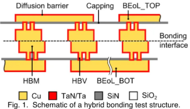
The test vehicle was manufactured by the direct bonding of two 300 mm-patterned wafers as described in [5]. In the present study, a 300 °C/1 h post bond anneal is applied to strengthen the bonding. The employed test structure consists of a 100-link daisy chain as illustrated in Fig. 1. The Hydrid Bonding Metal (HBM) has a dimension of 3.6 μm. The test structure has 16 Hybrid Bonding Vias (HBVs) in a form of a 4×4 matrix per single HBM.
Fig. 1. Schematic of a hybrid bonding test structure.
EM tests were performed at the package level on 19 samples. A temperature of 350 °C and an electric current of 20 mA were applied. This electric current leads to a current density of 0.57 MA/cm² in the BEoL_TOP layer and 1.39 MA/cm² at the HBV level if all the HBVs are considered to be connected in parallel. The failure criterion for the test stop condition and statistical study was set at 10 % of the resistance increase. Electrical resistance was monitored with the four-terminal sensing method during the EM test. Typical BEoL resistance degradation similar to the one shown in [8] was obtained.
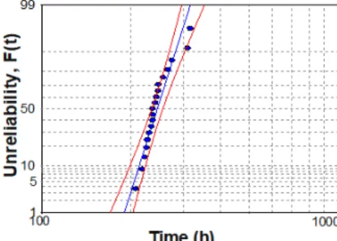
TTF was defined as the instance in time when the test structure has reached the 10 % increase in relative resistance. The obtained failure distribution shown in Fig. 2 fits well with the lognormal distribution with a correlation coefficient of 0.946.
P. Cloetens and J. C. Da Silva are with the European Synchrotron Radiation Facility, B. P. 220, 38043 Grenoble CEDEX, France.
F. Lorut and S. Lhostis are with STMicroelectronics, 850 rue Jean Monnet, 38926 Crolles, France.
Correlation between Electromigration-Related
Void Volumes and Time-to-Failure by High
Resolution X-Ray Tomography and Modeling
S. Moreau, A. Fraczkiewicz, D. Bouchu, P. Bleuet, P. Cloetens, J. C. Da Silva, H. Manzanarez, F. Lorut, and S. Lhostis
III. FAILURE ANALYSIS
A. Conventional physical failure analysis
Failure localization and following physical failure analyses were done on numerous samples by employing InfraRed (IR) imaging, lock-in thermography (LiT) and FIB/SEM cross-sectioning imaging. IR imaging combined with LiT analysis revealed the presence of only one suspicious location, at the anode side (I+) of the test structure. Fig. 3 shows the location of the defect and confirms it to be a void by means of FIB cross sectioning and SEM imaging. No EM-induced voids were found along the daisy chain probably due to the short line Blech effect [9]. Voids were localized only in the feed line (BEoL_TOP layer) above the via matrix at the anode side. It can be explained by the atomic flux divergence at the TaN/Ta barrier between HBVs and BEoL_TOP and the long length of the feed line (negligible Blech’s effect).
These results confirm that this type of hybrid bonding stack is immune to electromigration.
Since the 10 % increase of the test structure resistance is caused by voids, which are not occupying the entire cross section of the feed line, an advanced imaging technique is required for measuring these void volumes.
Fig. 2. Failure distribution after an electromigration test (350 °C, 20 mA) of 19 samples manufactured by hybrid bonding. Points: experimental times-to-failure. Blue line: fitted lognormal distribution (r²: 0.95). Red curves: confidence bounds at 90 %.
a)
b)
Fig. 3. Typical failure analysis results on a hybrid bonding sample after an electromigration test, a) I.R. imaging, one void is identified at anode side b) SEM imaging, void location is in BEoL_TOP layer.
B. Advanced failure analysis using high resolution synchrotron-based nano-tomography
To address the problem of void volume measurement and to avoid a complicated sample preparation procedures, synchrotron-based X-ray phase-contrast nano-tomography was employed [10]. The ID16A nano-imaging beamline of the European Synchrotron Radiation Facility (ESRF) was used [11]. The beam energy was fixed at 33.6 keV and the voxel size was 25 nm.
Most of the ID16A beamline pictures have a resolution of 2 to 3 pixels. The resolution is estimated by measuring the intensity profile on the edge of a sample for example. This approach leads to a metric resolution is in the range of: 50-75 nm (2-3 pixels @ 25 nm). Using a SEM/TEM analogy (see APPENDIX for the details), the ID16A beamline’s metric
resolution is in the range of: 27-129 nm (2-3 pixels @ 13-43 nm).
The ID16A beamline provides the required resolution and the field of view enabling detection of different failure locations (BEoL_TOP or BEoL_BOTTOM) [8] and to observe the bonding and EM induced voids with sizes ranging from hundreds of nanometer to tens of microns. However, as we need statistical information and fast results, some adjustments must be made in terms of workflow. The workflow adjustment (similar to the one described in [12]) has allowed us to employ synchrotron-based tomography for statistical studies, and to make it a tool for routine measurements.
Compared to the 19 samples stressed by electromigration, only 17 were characterized by X-ray tomography. After the tomographic reconstruction step, one can do virtual cross-sections to localize the depleted volume as illustrated in Fig 4-a/b. The depleted volume (Vdep) is clearly visible as it appears
in white. Due to the contrast difference between the metal and the void, the void volume segmentation was done easily as illustrated in Fig. 4-c/d. From the segmented voids, the depleted copper volumes were extracted. Depleted volume values span from 1.93 to 3.78 µm3, i.e. a 1:2 ratio (see Fig. 5). Fig. 4-a and
Fig.4-b have respectively the lowest and one highest depleted volumes. In addition, voids electrically disconnect from 8 to 15 HBVs. In other words, the failure criterion is reached for a large variety of void sizes.
a) c)
b) d)
Fig. 4. Illustrative tomography results after an electromigration test (350 °C, 20 mA). a-b) Automatically reconstructed slice and c-d) cavity
segmented volume (copper depleted volume). Sample in Fig. 4-a has the lowest depleted volume, while sample in Fig. 4-b has one of the highest.
IV. TTF AND VOID VOLUME CORRELATION
The measured Vdep have been paired with the corresponding
TTF. Fig. 5 shows the correlation between these two variables. A correlation analysis gives two important values: (i) a correlation coefficient of +0.85 indicating a strong linear relationship between the two variables, and (ii) a p-value of 0.000013 meaning the correlation is highly significant.
The slope of the fitted line (solid line in Fig. 5) gives the effective void volume growth rate of 0.015 µm3/h. It should be
noted that the measured resistance increase in test structures was caused by two factors, (i) via undercut, and (ii) reduction of the electric current conducting cross section by the void volume. Differences in grain structures and locations of the process-induced flaws, serving as precursors for void initiation, are responsible for the different sequences of HBV undercut and different volumes of voids leading to the 10 % increase in resistance, which was observed in different samples.
Fig. 5. Void volumes (copper depleted volume) vs. times-to-failure (TTF) after an electromigration test (350 °C, 20 mA) on hybrid bonding-based integration samples. A clear correlation exists.
V. MODELING
To further the understanding of the Vdep-TTF correlation, a
3D Finite Element Modeling (FEM) has been performed. The simulation domain consists of the weakest link of the daisy-chain under test (see Fig. 3 and Fig. 6-a). In a first approach, the electric simulation does not take into account temperature-dependent material properties or Joule heating. Fig. 6-b highlights the inhomogeneous distribution of the electrical current densities in the structure and points out that different HBVs make different contributions to the electric current flow. Consequently, if the growing void undercuts HBVs that conduct most of the electrical current, a large increase of electrical resistance is observed. The opposite is also true.
a)
b)
Fig. 6. a) 3D geometry for finite element modeling and b) distribution of the electrical current density in the underlying HBV matrix (bottom view) and in a part of the BEoL_TOP; the other layers are hidden for ease of understanding. An inhomogeneous distribution is visible.
To assess this scenario without going through the EM phenomena modeling (void nucleation and growth), we studied the influence of arbitrary fixed void volumes versus their location relative to the HBV matrix. A void is defined as a Cu-free volume spreading above a given number of HBVs which are consequently not electrically active. Identical void volumes, localized at different places (in the BEoL_TOP layer over the HBV matrix), lead clearly to different electrical resistance variations (see Table I). As an illustration, for a fixed void volume equivalent to 14 disconnected HBVs, the electrical resistance variation span from +1.023 to +1.934 %.
With these results, we confirm that the electrical resistance is sensitive to exact location and shape of the EM-induced void.
TABLEI
ELECTRICAL RESISTANCE VARIATION DUE TO VOIDING IN THE BEOL_TOP
LAYER FOR DIFFERENT VOID SIZES (IN TERMS OF NOT-ELECTRICALLY
-ACTIVE HBVS) AND LOCATION
Void size ΔR/R0 (%) Void size ΔR/R0 (%) Void size ΔR/R0 (%) 0 0 12 0.930 14 1.744 8 0.129 12 0.392 14 1.934 8 0.475 12 0.736 14 1.084 8 0.342 12 0.599 14 1.023 8 0.255 VI. CONCLUSION
In the framework of the development of Back-Side Illuminated CMOS Image Sensors (BSI CIS), experimental studies have demonstrated the electromigration (EM) resistant nature of the analyzed hybrid bonding-based test structures. EM failure occurs due to voiding in the contact area BEoL layer. A linear relationship was demonstrated between the void volume and time-to-failure. Due to non-uniform distribution of electric current in the region attached to the HBV matrix, the failure time is sensitive to exact location and shape of the EM-induced void. This observation is important for understanding the role of via redundancy, which is provided by using via matrixes, in increasing EM robustness of the interconnect.
APPENDIX
In the case of SEM/TEM, the thicker the sample, the lower the electrons penetrate [13]. Consequently, resolution degrades too. On the contrary, as X-ray have no charge, they interact infrequently with the materials they pass through and thus penetrate materials more easily. A rule-of-thumb for the relation between the expected spatial resolution and the sample thickness is given by: 𝑡 ≈!(∆$)& ! where t is sample thickness, Δr is spatial resolution and λ is the wavelength of the X-ray
photons [14]. So, for the energy of 33.6 kV of the incident X-ray photons and for a sample thickness ranging from 10 to 100 μm, one can expect a resolution from 13 to 43 nm, if the only source for resolution degradation is the sample thickness. ACKNOWLEDGMENT
Stéphane Moreau acknowledges Armen Kteyan and Valeriy Sukharev (Mentor, a Siemens Business) for fruitful discussions and constructive criticism of the manuscript.
REFERENCES
[1] Y. Kagawa, N. Fujii, K. Aoyagi, Y. Kobayashi, S. Nishi, N. Todaka, S. Takeshita, J. Taura, H. Takahashi, Y. Nishimura, K. Tatani, M. Kawamura, H. Nakayama, T. Nagano, K. Ohno, H. Iwamoto, S. Kadomura, and T. Hirayama, "Novel Stacked CMOS Image Sensor with Advanced Cu2Cu Hybrid Bonding," in International Electron
Devices Meeting (IEDM), 2016, pp. 8.4.1-8.4.4, DOI:
10.1109/IEDM.2016.7838375.
[2] J. Jourdon, S. Lhostis, S. Moreau, J. Chossat, M. Arnoux, C. Sart, Y. Henrion, P. Lamontagne, L. Arnaud, N. Bresson, V. Balan, C. Euvrard, Y. Exbrayat, D. Scevola, E. Deloffre, S. Mermoz, A. Martin, H. Bilgen, F. Andre, C. Charles, D. Bouchu, A. Farcy, S. Guillaumet, A. Jouve, H. Fremont, and S. Cheramy, "Hybrid bonding for 3D stacked image sensors: impact of pitch shrinkage on interconnect robustness," in 2018 IEEE International Electron
Devices Meeting (IEDM), 2018, pp. 7.3.1-7.3.4, DOI:
10.1109/IEDM.2018.8614570.
[3] J. R. Black, "Mass transport of aluminum by momentum exchange with conducting electrons," in Proceedings of the 6th Annual
Syrnposium Reliability Physics Symposium, 1967, pp. 148-159.
[4] C. S. Hau-Riege, "An introduction to Cu electromigration,"
Microelectronics Reliability, vol. 44, pp. 195-205, Feb 2004, DOI:
10.1016/j.microrel.2003.10.020.
[5] S. Lhostis, A. Farcy, E. Deloffre, F. Lorut, S. Mermoz, Y. Henrion, L. Berthier, F. Bailly, D. Scevola, F. Guyader, F. Gigon, C. Besset, S. Pellissier, L. Gay, N. Hotellier, A. L. Le Berrigo, S. Moreau, V. Balan, F. Fournel, A. Jouve, S. Cheramy, M. Arnoux, B. Rebhan, G. A. Maier, and L. Chitu, "Reliable 300 mm Wafer Level Hybrid Bonding for 3D Stacked CMOS Image Sensors," in Electronic
Components and Technology Conference (ECTC), 2016, pp.
869-876, DOI: 10.1109/Ectc.2016.202.
[6] E. Arzt, O. Kraft, W. D. Nix, and J. E. Sanchez, "Electromigration failure by shape change of voids in bamboo lines," Journal of
Applied Physics, vol. 76, pp. 1563-1571, August 1994, DOI:
10.1063/1.357734.
[7] H. Tsuchiya and S. Yokogawa, "Electromigration lifetimes and void growth at low cumulative failure probability," Microelectronics
Reliability, vol. 46, pp. 1415-1420, September-November 2006,
DOI: 10.1016/j.microrel.2006.08.001.
[8] S. Moreau, D. Bouchu, V. Balan, A. L. Le Berrigo, A. Jouve, Y. Henrion, C. Besset, D. Scevola, S. Lhostis, F. Guyader, E. Deloffre, S. Mermoz, and J. Pruvost, "Mass transport-induced failure of hybrid bonding-based integration for advanced image sensor applications," in Electronic Components and Technology
Conference (ECTC), 2016, pp. 1940-1945, DOI:
10.1109/Ectc.2016.27.
[9] I. A. Blech, "Electromigration in Thin Aluminum Films on Titanium Nitride," Journal of Applied Physics, vol. 47, pp. 1203-1208, April 1976, DOI: 10.1063/1.322842.
[10] P. Cloetens, W. Ludwig, J. Baruchel, D. V. Dyck, J. V. Landuyt, J. P. Guigay, and M. Schlenker, "Holotomography: Quantitative phase tomography with micrometer resolution using hard synchrotron radiation x rays," Applied Physics Letters, vol. 75, pp. 2912-2914, November 1999, DOI: 10.1063/1.125225.
[11] J. Cesar da Silva, A. Pacureanu, Y. Yang, S. Bohic, C. Morawe, R. Barrett, and P. Cloetens, "Efficient concentration of high-energy x-rays for diffraction-limited imaging resolution," Optica, vol. 4, pp. 492-495, May 2017, DOI: 10.1364/OPTICA.4.000492.
[12] A. Fraczkiewicz, P.-O. Autran, E. Capria, P. Cloetens, J. Da Silva, S. Lhostis, F. Lorut, S. Moreau, T. Mourier, and P. Bleuet, "Making synchrotron tomography a routine tool for 3D integration failure analysis through a limited number of projections, an adapted sample preparation scheme, and a fully-automated post-processing," in
International Symposium on Testing and Failure Analysis,
Pasadena, CA, USA, 2017, pp. 14-18.
[13] K. Kanaya and S. Okayama, "Penetration and energy-loss theory of electrons in solid targets," Journal of Physics D: Applied Physics, vol. 5, pp. 43-58, 1972/01/01 1972, DOI: 10.1088/0022-3727/5/1/308.
[14] J. M. Rodenburg and R. H. T. Bates, "The theory of super-resolution electron microscopy via Wigner-distribution deconvolution,"
Philosophical Transactions of the Royal Society of London. Series A: Physical and Engineering Sciences, vol. 339, pp. 521-553,