HAL Id: hal-01242389
https://hal.archives-ouvertes.fr/hal-01242389
Submitted on 30 Nov 2016
HAL is a multi-disciplinary open access
archive for the deposit and dissemination of
sci-entific research documents, whether they are
pub-lished or not. The documents may come from
teaching and research institutions in France or
L’archive ouverte pluridisciplinaire HAL, est
destinée au dépôt et à la diffusion de documents
scientifiques de niveau recherche, publiés ou non,
émanant des établissements d’enseignement et de
recherche français ou étrangers, des laboratoires
Quantum confinement and dielectric profiles of colloidal
nanoplatelets of halide inorganic and hybrid
organic-inorganic perovskites
Daniel Sapori, Mikael Kepenekian, Laurent Pedesseau, Claudine Katan, Jacky
Even
To cite this version:
Daniel Sapori, Mikael Kepenekian, Laurent Pedesseau, Claudine Katan, Jacky Even.
Quantum
confinement and dielectric profiles of colloidal nanoplatelets of halide inorganic and hybrid
organic-inorganic perovskites. Nanoscale, Royal Society of Chemistry, 2016, Themed Collection ”Perovskites
at the nanoscale: from fundamentals to applications”, 8 (12), pp.6369-6378. �10.1039/C5NR07175E�.
�hal-01242389�
Quantum confinement and dielectric profiles of colloidal nanoplatelets
of halide inorganic and hybrid organic-inorganic perovskites
†
Daniel Sapori,
aMika¨el Kepenekian,
⇤bLaurent Pedesseau,
aClaudine Katan,
bJacky Even
⇤a Received Xth XXXXXXXXXX 20XX, Accepted Xth XXXXXXXXX 20XXFirst published on the web Xth XXXXXXXXXX 200X DOI: 10.1039/b000000x
Quantum confinement as well as high frequencye• and statices dielectric profiles are described for nanoplatelets of halide
inorganic perovskites CsPbX3 (X = I, Br, Cl) and hybrid organic-inorganic perovskites (HOP) in two-dimensional (2D) and
three-dimensional (3D) structures. 3D HOP are currently sought for their impressive photovoltaic ability. Prior to this sudden popularity, 2D HOP materials were driving intense activity in the field of optoelectronics. Such developments have been enriched by the recent ability to synthesize colloidal nanostructures of controlled size of 2D and 3D HOP. This raises the need to achieve a thorough description of the electronic structure and dielectric properties of these systems. In this work, we go beyond the abrupt dielectric interface model and reach atomic scale description. We examine the influence of the nature of the halogen and of the cation on the band structure and dielectric constants. Similarly, we survey the effect of dimensionality and shape of the perovskite. In agreement with recent experimental results, we show an increase of the band gap and a decrease ofe•
when the size of a nanoplatelet reduces. By inspecting 2D HOP, we find that it cannot be described as a simple superposition of independent inorganic and organic layers. Finally, the dramatic impact of ionic contributions on the dielectric constantesis
analysed.
Introduction
Solution-processed three-dimensional (3D) halide perovskites of general formula RMX3 (M = Pb, Sn, Ge and X = I, Br,
Cl, Fig. 1-a) have become, over the last three years, photo-voltaics superstars, provided that the cation R is an organic cation (e.g. methylammonium CH3NH+3). Indeed, hybrid
organic-inorganic perovskites (HOP) based solar cells have shown power conversion efficiencies growing from 3.8% in 20091to over 20% in 2015.2In addition to impressive
perfor-mances, HOP offer easy processability (low temperature, full solution process) and thus open the way towards low cost pro-duction of high-efficiency solar cells.
As far as chemistry is concerned, these materials offer a chemical playground. Depending on the choice of the metal, the anion or the organic cation, HOP crystallize in various structures. Thus, chemical engineering offers the possibility to tune properties such as band gaps.3,4In particular, the
struc-ture is sensitive to the size of the organic cation. For molec-ular ions ‘large enough’ (e.g. C4H9NH+3), the compound is
† Electronic Supplementary Information (ESI) available: Complementary results on the electronic structure and dielectric constants of CsPbX3 and CH3NH3PbX3(X = I, Br, Cl). See DOI: 10.1039/b000000x/
a Universit´e Europ´eenne de Bretagne, INSA, FOTON UMR 6082, 35708 Rennes, France; E-mail: jacky.even@insa-rennes.fr
b Institut des Sciences Chimiques de Rennes, UMR 6226, CNRS - Univer-sit´e de Rennes 1, Campus de Beaulieu, 35042 Rennes, France; E-mail: mikael.kepenekian@univ-rennes1.fr
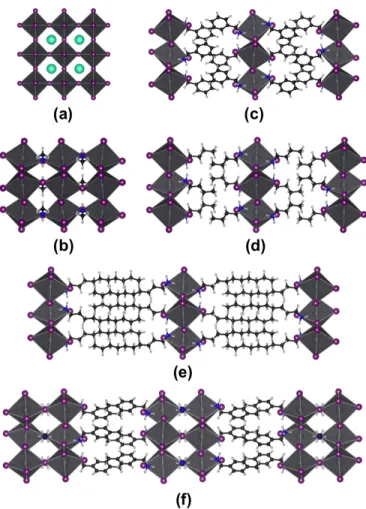
Fig. 1 Schemes of (a) 3D halide perovskite, (b) 2D hybrid
organic-inorganic halide perovskite, and (c) colloidal nanoplatelet of hybrid organic-inorganic halide perovskite. Grey circles stand for metal cations (Pb, Sn, Ge), purple circles for halides (I, Br, Cl), and blue circles for inorganic (Cs) or organic cations.
organized as a two-dimensional (2D) structure with an organic layer buffering inorganic slabs (Fig. 1-b). Incidentally, intense investigations on HOP started more than two decades ago when Mitzi and coworkers designed thin-film transistors based on 2D HOP.5,6 Up to 2009, solar cell applications, although
an-ticipated, were not pursued and HOP became popular in the field of optoelectronics for production of transistors and light-emitting devices.7–11In addition to these bulk 2D and 3D
mate-rials, nanostructures of perovskites, e.g. colloidal nanoplatelets (CNPL, Fig. 1-c), have recently been reported.12–20
prop-erties. 2D HOP are known to present a strong exciton binding energy21related to abrupt dielectric interfaces22and exhibit a
quantum confinement of type I23,24 with a dielectric
confine-ment22,25 attributed to the contrast between the low dielectric
constant of the organic part26 and the high dielectric constant
of the inorganic part.27On the other hand, 3D HOP show an
ex-citon screened by polar vibrational modes and disordered con-figurations of polar organic cations.28–31The acquired control
over the shape of the active materials allows one to tune quan-tum and dielectric confinements. The later is a crucial point as it has a direct impact on the binding energy of the exciton32
and thus, influence the separation and the transport of charges. Quantum size effects of HOP nanoplatelets of different thick-nesses were investigated experimentally and an increase of the energy gap and of the exciton binding energy was observed for the thinner nanoplatelets.20 Theoretical inspections can shed
light on these effects. In a pioneer contribution, Muljarov et al. calculate the binding energies of excitons in HOP.33 This
method takes into account the dielectric confinement but relies on parameters fitted to experimental data. Moreover, to avoid unphysical divergences related to abrupt dielectric interfaces, a transitional layer at the interface between organic and inorganic parts has to be considered. Recently, we proposed a different approach based on density functional theory (DFT) calculations to describe dielectric profiles of 2D systems.34 Our method
takes advantage of the ab initio description of the nanoplatelets and in particular of interfaces.
In this work, we use DFT calculations and subsequent treat-ments to describe the quantum and dielectric confinetreat-ments in halide perovskite-based nanostructures. We start by recalling the main features of the method. Then, we describe the quan-tum confinement in 3D all-inorganic perovskites CsPbX3(X =
I, Br, Cl) nanoplatelets as well as the most studied 3D HOP CH3NH3PbX3(X = I, Br). The confinement effects are
com-pared to the one observed in 2D and intermediate (2D/3D) materials. In all cases, the expected enlargement of the band gap is observed when going to thinner systems. Then we dis-cuss static and high frequency dielectric profiles and find a di-electric confinement for systems where the inorganic layer is less than 30 ˚A. In agreement with recent experimental data, we show a decrease of the dielectric constant with decreasing nanoplatelets thicknesses.
Methods
Computational details
First-principles calculations are based on DFT as implemented in the SIESTA package.35,36 Calculations have been carried
out with the GGA functional in the PBE form.37 Atoms
are described by scalar relativistic norm-conserving Troullier-Martins pseudopotentials,38 that include 14 valence electrons
for Pb, 7 for I, 5 for N, 4 for C and 1 for H. Valence wave func-tions are described through a basis set of finite-range numer-ical pseudoatomic orbitals.39 Structures relaxation and
elec-tronic structure calculations have been done using a double-z polaridouble-zed basis sets.39 The geometries were optimized
un-til the forces were smaller than 0.01 eV. ˚A 1. The electronic
structure was converged using a 1 ⇥ 4 ⇥ 4 k-point sampling of the Brillouin zone. In all cases, an energy cutoff of 150 Ry for real-space mesh size has been used. After construction, the atomic positions of the slabs of CsPbX3, CH3NH3PbI3and
CH3NH3PbBr3are first relax (along the [010] direction) in the
absence of any electric field. These optimized structures are then used as the starting point to compute the electronic and di-electric properties. The high frequency didi-electric constants are obtained by relaxing the sole electron density under the external electric field, keeping the atomic positions fixed. To compute the static dielectric constant, the atomic positions are relaxed both in the absence and in the presence of the electric field. The choice of the magnitude of the external electric field is made based on a compromise between large enough variation of the electron density and absence of higher-order contributions (e.g. 0.1 V. ˚A 1).
Let us note that spin-orbit coupling (SOC) is not taken into account in the present calculations. Although it is knows to be of importance for the description of the electronic structure of HOP (especially for lead-based HOP), it leads to significant un-derestimation of the band gap.25,40–44In turn, this would lead to
an artifactual overestimation of the dielectric constant and arti-facts in the calculated profiles. Adding many-body corrections, such as in SOC+GW calculations, would provide an improved alternative. Unfortunately, this level of theory has a much larger computational cost, thereby preventing the investigation of lay-ered structures or colloidal nanoplatelets.
Dielectric profiles
Despite the importance of the dielectric constant, its descrip-tion often relies on a crude continuum modeling of the dielec-tric heterostructures by abrupt interfaces, with one dielecdielec-tric constant value for the semiconductor core and another one for the surfaces and the surrounding medium.45–47Alternative Ab
initio-based approaches of interfaces have also been proposed, based on DFT calculations of free-standing silicon/oxyde and ferroelectric slabs48,49 or other heterostructures.50 These
ap-proaches rely on periodic supercells, a plane wave description of the wavefunction and are included in the self-consistent part of widely used first-principles codes such as VASP51or
Quan-tum ESPRESSO.52Next, taking advantage of the strictly
local-ized basis set description available in the SIESTA code,35,36
of-fers another type of approach to the determination of dielectric profiles (see ESI†).34,53,54Such an approach is computationally
vacuum and is parameter free. Here we recall the main points of the latter method, more details can be found in Ref. 34.
Similarly to the scheme introduced by Giustino and cowork-ers,55 dielectric profiles are obtained without the description
of the whole dielectric matrix, thus reducing the computational time. The induced variation of the planar averaged electron density, drind(z), is given by drind(z) =r(z)|~Eext r(z)|0,
where ~Eext is an external electric field. Longitudinal nanoscale
and transverse macroscopic averages are performed to derive nanoscale dielectric properties.34,53,54This is important to
en-sure proper connection with the macroscopic dielectric constant of the bulk material.
Applying an electric field is performed on slabs which are periodically reproduced. Thus, the induced polarization shall be corrected for unphysical inter-slab interactions. This can-not be performed directly on the induced polarization. A trick is to calculate the total induced dipole mz(L) for various
inter-slab distances L with and without the external electric field. The slope of the inverse of mz(L) as a function of 1/L is equal
to 1/(e0.Eext), wheree0is the vacuum permittivity.53 The
in-duced dipole mz (L ! •) for an infinite L, is simply obtained
by extrapolating 1/L to 0. The ratio mz(L ! •)/mz(L) is then
employed to correct the induced polarization from the artificial interaction between the slabs.
Four steps are required to derive the dielectric constant pro-files along the stacking axis of the slab from the calculated DFT electron density:
(i) The electron density has first to be averaged in the plane perpendicular to the stacking axis. The electron density profiler(z) is then smoothed using a nanoscale averaging along the stacking axis.56The length of the filter function
is chosen from the study of the Hartree potential profile. For perovskites investigated in this works, it is equal to the distance between two adjacent octahedra. This is in good agreement with the definition of macroscopic inter-nal fields in a solid (vide infra).
(ii) Compute the induced electron density from the DFT computations with and without an external electric field: drind(z) =r(z)|~Eext r(z)|0.
(iii) Compute the induced polarization pind(z) by partial
inte-gration of the induced electron density d pind(z)
dz = drind(z).
and correct for the unphysical inter-slab interaction using the ratio mz(L ! •)/mz(L). The total induced dipole is
given by
mz=
Z z
•pind(z)dz.
(iv) Derive the nanoscopic average of the dielectric constant profilee(z) from the induced polarization
e•(z) =e e0Eext 0Eext pind(z).
The dielectric constant depends on the frequency of the elec-tric field, the temperature and the direction. It is usually de-scribe by a tensor when the system is anisotropic. In the high frequency limit (e•), it takes into account only the distortion
of the electron density by the electric field. For lower fre-quencies (es) it takes into account both electronic and ionic
effects (phonons). For extremely low frequencies, other inter-actions such as dipolar interinter-actions contribute as well. In the present work, the latter are not included in our computation of es. Moreover, as we use a static electric field, we are bound
to the description of limit cases. The inspection of intermedi-ate regimes would involve the use of time-dependent electric field and of more sophisticated approaches that are generally dedicated to the study of laser-irradiated materials.57–61
Investigated structures
First, we consider the all-inorganic perovskites CsPbX3(X = I,
Br, Cl) series. Recently, synthesis of colloidal nanocrystals and nanoplatelets of these compounds has been reported.17,62
Start-ing from the Pm¯3m cubic phase (no. 221),63we construct slabs
with thicknesses going from 1 to 8 layers, each layer consisting in an octahedra PbI6stacked in the [001] direction (Fig. 2-a).
Similar slabs are constructed from the low-temperature Pnma (no. 62) phase of CH3NH3PbI3 and CH3NH3PbBr3 (Fig.
2-b)64,69in the [010], [100] and [001] direction.
A series of 2D HOP are then explored (Fig. 2-c-e). In those systems a one-octahedron thick inorganic layer is sand-wiched between layers of organic cations. The effect of the molecule on the confinement is inspected. The or-ganic cation is aromatic for (C7H10N)2PbI4,65 aliphatic for
(C4H12N)2PbI4and (C10H24N)2PbI4.66,67 Finally, the 2D/3D
HOP (C10H24N)2PbI3CH3NH3PbI4is investigated (Fig. 2-f).68
In this system, the inorganic layer is 2-octahedron thick.
Results and discussion
Quantum confinement in nanoplatelets
We first stress that it is well known that semiconductor band gaps are poorly reproduced by plain DFT calculations (vide in-fra). However, the qualitative trends are well reproduced and comparisons between similar structures can be conducted.
Bulk CsPbX3 (X = I, Br, Cl) in the Pm¯3m phase presents
a direct band gap at R (Fig. S1, ESI†).70–72The main impact
climbing down the halogen column is the reduction of the band gap that goes from 2.54 eV for CsPbCl3to 1.73 eV for CsPbI3
Fig. 2 Structures of (a) all-inorganic CsPbX3(X = I, Br, Cl) in the
Pm¯3m phase,63(b) the 3D HOP CH3NH3PbI3in the
low-temperature Pnma phase,64a series of 2D HOP with (c)
aromatic organic cation (C7H10N)2PbI4,65(d) and (e) aliphatic
organic cation (C4H12N)2PbI4, and (C10H24N)2PbI4,66,67
respectively and (f) the 2D/3D-HOP
(C10H24N)2PbI3CH3NH3PbI4.68Pb, Cs, I, N, C and H atoms are
depicted in gray, green, purple, blue, black and white, respectively.
(Table 1). When going to slabs of CsPbX3, the cubic
symme-try is lost and the R and M points become equivalent. Fig. 3-a presents the band structure of CsPbI3slabs for various
thick-nesses. The expected behavior is retrieved when going to thin-ner slabs: the band gap increases from 1.79 eV to 1.94 eV un-der the effect of quantum confinement (Fig. 3-b). For a 8-layer slab, the bulk band gap is nearly recovered, i.e. the confinement vanishes. The relative increase of the band gap due to quantum confinement becomes slightly larger for Br and Cl based per-ovskites (Table 1 and Fig. S2, ESI†) with band gaps varying from 2.11 to 2.32 eV and 2.50 to 2.75 eV, respectively. These results are consistent with recent experimental data reporting an increase of the band gap energy with the reduction of the semiconductor CsPbX3core of the QD.62
Table 1 Calculated band gap (eV) for bulk and slabs of all inorganic and organic-inorganic perovskites.
Cation Cs+ CH 3NH+3 Halogen I Br Cl I Br Bulk 1.73 2.11 2.54 2.05 2.50 8-layer 1.79 2.11 2.50 2.07 2.44 4-layer 1.85 2.19 2.60 2.15 2.51 2-layer 1.94 2.27 2.68 2.31 2.60 1-layer 1.93 2.32 2.75 2.48 2.77
With the organic cation CH3NH+3, the band structure of
nanoplatelets (Fig. 4-a) shows a direct band gap at theG point, as in the corresponding Pnma bulk.11,40,43,44,73 Again, when
decreasing the size of the slab, the band gap increases, going from 2.07 eV for the 8-layer slab to 2.48 eV for the 1-layer slab. The effect of quantum confinement becomes significant for slabs formed of less than 4 layers (Table 1 and Fig. 4-b). Slabs of CH3NH3PbBr3follow the same trend (Fig. S3, ESI†)
with band gaps varying from 2.44 to 2.77 eV.
The variation of the band gap of all-inorganic and hybrid per-ovskite slabs with the number of layers N can be expressed as
Eg(N) = Eg,bulk+dEg(N),
where Eg(N) is the band gap of the bulk core material and
dEg(N) stems from quantum and dielectric confinement
ef-fects.
The various contributions can be estimated from theoretical calculations by using the following decomposition:
Eg(N) = Eg,DFT,bulk+dEg,DFT(N) +Sbulk+dS(N),
where Eg,DFT,bulk andSbulkare respectively the bulk band gap
evaluated at the DFT level and the self-energy corrections due to many-body effects. The self-energy corrections are very of-ten computed with the GW approximation. For lead-based per-ovskites, the various contributions should in principle include SOC effects.
The effect of quantum confinement can be estimated from dEg,DFT(N), provided that the effective masses of the bulk
ma-terials are accurately described by plain DFT calculations. In the case of CH3NH3PbI3, due to error cancellation, the DFT
electronic band gap and effective masses are fortuitously in quite good agreement with GW+SOC values. For this reason, thedEg,DFT(N) computed without SOC (Fig. 4) yield good
es-timates of the effect of quantum confinement.
Due to limited available computational power, the variation of the self-energy with the number of layers,dS(N), cannot be evaluated directly from GW computations. An alternative semi classical evaluation of this self-energy correction will later on be given within the framework of the dielectric confinement theory (vide infra).
Fig. 3 (a) Band structures for slabs of CsPbI3. (b) Band gaps with
respect to the slab thickness for CsPbX3(X = I, Br, Cl).
Experimentally, such effects were observed for CH3NH3PbI3 and CH3NH3PbBr3 nanoobjects.15,16,20
How-ever, Sichert et al. notice that for colloidal nanoplatelets the optical band gap evolution does not show the sudden variation anticipated by various models and also observed in our DFT results.20 This supports an increase of the exciton binding
energy in thinner slabs that may compensate the expected band gap enlargement related to quantum confinement. It prompts further inspection of dielectric confinement in such structures.
The behavior of the all-inorganic and hybrid perovskites nanoplatelets are qualitatively similar with respect to quantum confinement. As expected, the band gap increases when the thickness of the slab decreases. This effect gets stronger when the halogen is lighter (Cl > Br > I). However, all these obser-vations are much more pronounced in the case of an organic cations that emphasize quantum confinement.
High frequency dielectric profile
The high dielectric profiles e•(z) of CsPbI3 is depicted in
Fig. 5-a. In the case of a large slab (8 layers), the bulk di-electric constant is recovered at its center amounting to 5.0. The same is observed for CsPbBr3and CsPbCl3(Fig. S4, ESI†)
Fig. 4 (a) Band structures for slabs of CH3NH3PbI3with various
thicknesses. (b) Band gaps with respect to the slab thickness for CH3NH3PbX3(X = I, Br).
with bulk-like dielectric constants of 3.8 and 3.2, respectively. In the case of CsPbCl3, the dielectric constant has
experimen-tally been determined and ranges between 3.6 and 3.7,74in fair
agreement with our computed value. The reduction of the slab thickness leads to a decrease of the dielectric constant (Fig. 5-a and Fig. 6) that tends to converge to the medium value 1. Di-electric properties significantly different from those of the bulk material are observed for slabs of less than 4 layers with a more pronounced variation when going from chlorine to iodine.
The substitution of Cs+by the organic cation CH
3NH+3 in
the 3D HOP structure leads to an enhancement of the dielec-tric constant (Fig. 5-b). For slabs constructed in the [010] di-rection, the dielectric constant at the center converges to 5.6 for thick enough slabs. The low temperature Pnma phase is not isotropic and one has to inspect all directions. We find that the dielectric constant reaches 4.9 and 4.8 for slabs ori-ented along [100] and [001], respectively (Fig. S5, ESI†). The average value e•=5.1, compares well with the experimen-tal value of 6.5 measured on the Pmma phase75and to
previ-ous values obtained by DFT+SOC for different orientations of the cation76or GW+SOC calculations.42 For CH
3NH3PbBr3,
a bulk value of 4.2 is found. One can notice that the halogen 5
Fig. 5 High frequency dielectric profiles e•(z) for slabs of (a)
CsPbI3, (b) CH3NH3PbI3(in the [010] direction). Black, orange, red and blue lines correspond to 1, 2, 4 and 8-layer slabs, respectively. e•(z) for (c) the 2D HOP with aromatic cation C7H10N)2PbI4, the
2D HOP with aliphatic cations (d) (C4H12N)2PbI4, and (e)
(C10H24N)2PbI4. (f) Same for the 2D/3D HOP
(C10H24N)2PbI3CH3NH3PbI4.
influence remains the same whatever the nature of the cation (e•CsPbBr3(0)/eCsPbI• 3(0) ⇡ e•CH3NH3PbBr3(0)/e•CH3NH3PbI3(0)).
As in the all-inorganic materials, the size reduction of CH3NH3PbI3nanoplatelets shows a dielectric confinement for
slabs of less than 4 layers, resulting in a e•(0) of 4.2 for
the 1-layer platelet (Fig. 5-b and Fig. 6). The same is ob-served with slabs of CH3NH3PbBr3(Fig. 6 and Fig. S6, ESI†)
with value going from 4.2 to 3.3 for the thinnest nanoplatelet. These results indicate that little or vanishing dielectric confine-ment is expected for all-inorganic perovskites CsPbX3or HOP
CH3NH3PbX3 (X = I, Br, Cl) with thicknesses larger than 4
layers.
In the case of 2D HOP, the profiles of the high frequency di-electric constant present a clear didi-electric contrast between the low dielectric constant of the organic part and the high dielec-tric constant of the inorganic part (Fig. 5-c to e). For all 2D materials, the value obtained for the inorganic part is around 4 (Table S2, ESI†). As expected, this value is lower than the bulk value of 3D materials (e.g. CH3NH3PbI3) and closer to
Fig. 6 High frequency dielectric constant at the slab centre e•(0) for
CsPbX3(X = I, Br, Cl) and CH3NH3PbX3(X = I, Br) in the [010]
direction.
the value obtained for 1-layer slabs of 3D HOP (Fig. 5-b, Ta-ble S1, ESI†). The dielectric constant obtained for the aromatic cation (Fig. 5-c) amounts to 2.9 and is higher than the one ob-tained for the aliphatic chains, 2.1 (Fig. 5-d and e). The later is in agreement with the experimental high frequency dielectric constant reported to be about 2.2-2.3.26Thus, if the size of the
aliphatic chain affects the extent of the low dielectric constant zone, it does not seem to modify significantly the value of the constant itself.
Finally, Fig. 5-f shows the dielectric profile of the 2D/3D compound (C10H24N)2PbI3CH3NH3PbI4. Interestingly, the
di-electric constant in the inorganic layer amounts to 4.8, which lies in between the value calculated for the purely 3D and purely 2D bulk systems. As in the 2D cases discussed above, the value is close, but slightly lower, than the value computed for a 2-layer platelet of CH3NH3PbI3(Fig. 5-b).
From our results, the nature of the cation (inorganic vs. or-ganic) has little influence on the high frequency dielectric pro-files of 3D perovksites. Indeed, the amplitude of the confine-ment effect is of the same order even if the dielectric constant is about 1.2 times larger. For both cases, specific dielectric prop-erties are observed for nanoplatelets of less than 4 layers. In addition, similar effects show up in the inorganic layers of 2D HOP.
Static dielectric profile
When the frequency of the electric field becomes lower, atoms can move and participate to the polarization of the slab. Thus, an ionic contribution to the dielectric constant has to be taken into account. For a low frequency dependent electric field, it corresponds to the additional contribution of the polar phonons. Here, the electric field is applied in the stacking direction of
the slab. Fig. 7 shows the atomic displacement caused by an electric field on a CH3NH3PbI3slab. It highlights the
shrink-ing and stretchshrink-ing of lead-iodine bonds in the stakshrink-ing direction, which correspond to the main electric field induced distortions. Under electric field, halogen-lead bonds alternate between long
Fig. 7 Modification of the I-Pb bonds in a 6-layer of CH3NH3PbI3
slab induced by an electric field.
and short. Concomitantly, an asymmetry shows up, and more specifically a loss of inversion symmetry. Therefore, each oc-tahedron bears an induced dipole that participates to the global dipole and polarization of the slab. This can be related to the bulk phonon contribution. In addition, organic cations at sur-faces are free to rotate and therefore naturally align with the electric field, leading to a specific contribution from surface phonons.
The dielectric profileses(z) of 6-layer and 1-layer slabs of
CsPbI3(Fig. 8-a) show the dramatic impact of the ionic
con-tribution on the dielectric constant. At the center of the 6-layer slab, it gets multiplied by a factor of 7 increasing frome•=5.0
to a value oscillating around 35. Large surface effects can be observed with the inorganic cation Cs+andes reaches values
beyond 60. Confinement leads to a strong reduction of es to
22.6 for the thinnest nanoplatelet.
When replacing the inorganic cation by an organic cation, for instance CH3NH+3, the dielectric profile ofesbecomes
vis-ibly smoother (Fig. 8-b). In fact, the surface coating by or-ganic moieties cancels the abrupt increase of the dielectric con-stant near the surface. A similar behavior has been observed with CdSe CNPL passivated by acetates.34The surface organic
cation are reoriented under the effect of the external electric field and tend to screen its effects. As a consequence, the di-electric constant does no more endure a seven-fold increase but a four-fold growth frome•=5.6 toes=22.0 at the centre of
the 6-layer slab (in the [010] direction). Unfortunately, compar-ison to experimental results is difficult. In fact, various experi-mental values have been reported for the static (low) frequency dielectric constant of bulk CH3NH3PbI3, which depend on the
sample (type/quality), temperature and on the method chosen: 28.8,7723.3,78and 3579for the tetragonal phase at room
tem-perature and 36 for the orthorhombic phase.78 However, we
find a better agreement with the increase of the reported bulk values ofe when the ionic displacements start having
signifi-Fig. 8 Static dielectric profile es(z) for slabs of (a) CsPbI3and (b)
CH3NH3PbI3(in the [010] direction). Black and red lines correspond
to 1 and 6-layer slabs, respectively.es(z) for (c) the 2D HOP with
aliphatic cations (C4H12N)2PbI4, and (d) the 2D/3D HOP
(C10H24N)2PbI3CH3NH3PbI4.
cant contributions to the dielectric constant of the slab. When the confinement is extreme (1-layer slab), the dielectric con-stant is essentially dominated by surface effects. At the same time, it still shows significant increase as compared to its high frequency value (Fig. 5-b), but reduces to 14.1 (Fig. 8-b).
The static dielectric profile of the 2D HOP (C4H12N)2PbI4
shows a remarkable feature (Fig. 8-c). The dielectric constant of the organic layer is roughly speaking not affected by the ionic contribution (e•=2.1 vs. es=2.4). On the other hand,
the dielectric constant of the inorganic part is 2.5 times larger in the static regime (es=9.5) than in the high frequency one
(e•=3.9). It traces back to the anisotropy of 2D materials
with the organic part that softens the displacement of the inor-ganic part. This reinforces the idea that 2D HOP are compos-ite materials with specific properties,24 including mechanical
properties with region of hard and soft elastic constants. Be-sides, the maximum value obtained for this 2D material is much lower than the value obtained for the 1-layer slab of the 3D HOP (Fig. 8-b). The organic moieties are indeed different. But, as it had already been stressed for quantum confinement,24, in
real 2D HOP structures the inorganic layer cannot be solely ap-proximated by a single standalone layer derived from the 3D material.
A similar behavior is obtained for the 2D/3D HOP (C10H24N)2PbI3CH3NH3PbI4 (Fig. 8-d). The dielectric
con-stant of the inorganic part is around 15, showing a great en-hancement with respect to the high frequency valuee•=4.8 (Fig. 5-f). As in the case of 2D HOP, the motion of atoms changes only modestly the dielectric constant of the organic layeres=3.3 vs.e•=2.9.
Dielectric confinement
In layered heterostructures and slabs, the classical evaluation of the dielectric self-energy correction is related to a self-energy profile:
dS(z0) =4pe0
Z •
0 (V (q,z,z0) Vbulk(q,z,z0))z!z0qdq.
where e0 is a test charge at position z0. dS(z0)is equivalent
to the one particle potential profile acting on the test charge. The electrostatic potential felt by a particle located at z0 in a
layered structure is computed by solving the inhomogeneous Poisson equation including the dielectric constant profilee(z):
∂ ∂z ✓ e(z)∂z∂ (V (q,z,z0)) ◆ q2e(z)V(q,z,z 0) = e0d(z z0).
The self-energy profiledS(z0)is plotted in Fig. 9-a for
var-ious slabs of CH3NH3PbI3. The shapes of the self-energy
profiles are consistent with our previous study on colloidal nanoplatelets of II-VI semiconductors, where maximum values are observed at the interfaces between the platelets and vac-uum.34Moreover, the value of the self-energy increases at the
center of the slab with decreasing thickness: this corresponds to the dielectric confinement effects. In addition, a semi-classical evaluation of the self-energy correction to the electronic band gap can be obtained, both for the CB and the VB states, by computing the following integrals:
dSCB(V B)(N) =
Z
dS(z,N)rCB(V B)(z,N)dz,
whererCB(V B)is the electronic density profile for the CB (VB)
state. The sum of these two terms undergoes a steep increases for very thin slabs. This effect can be estimated by plotting the value of the self-energy at the center of the slab as a function of the number of layers (Fig. 9-b). We can thus conclude that the dielectric confinement effect is very important up to four layers.
Finally, we shall point out that the actual band gap ob-tained from optical absorption measurements, may undergo a smoother variation than the band gap predicted from the com-putation of monoelectronic states. Indeed, the optical band gap corresponds to the electronic band gap minus the exciton bind-ing energy. The exciton bindbind-ing energy increases, when the thickness decreases, which partially compensates the gap in-crease related to quantum and dielectric confinement effects (vide supra) on the monoelectronic states.34,47
Conclusion
In summary, quantum confinements and dielectric confine-ments have been investigated for lead halide perovskites with
Fig. 9 (a) Self-energy profile dS(z) for slabs of CH3NH3PbI3. (b)
Self-energy taken at the slab centredS(0).
inorganic (Cs+) and organic (CH
3NH+3) cations for various
halogens. An increase of the band gap and a decrease of the dielectric constant occurs upon reducing the thickness of the nanoplatelets. Both quantum and dielectric confinements are predicted to show up for slabs counting less than 4 octahedra in the stacking direction. Dielectric properties in 2D and 2D/3D materials are discussed as well. In all cases, the dramatic effect of phonons on the dielectric constant has been illustrated with a great enhancement for the inorganic parts of the materials. This study is a first step towards the computation of self-energy cor-rections34that are necessary to reach an accurate description of
the exciton in these hybrid materials. Devices involving HOP imply an interface with other semiconductors, e.g. TiO2.80,81
As with 2D HOP materials, a dielectric contrast can then have dramatic effects. These interfaces will be the focus of upcom-ing studies.
Acknowledgement
This work has been supported by University of Rennes 1 (Action Incitative, D´efis Scientifiques Emergents 2015). It was performed, in part, at the Center for Integrated Nan-otechnologies, an Office of Science User Facility operated for the U.S. Department of Energy (DOE) Office of
Sci-REFERENCES REFERENCES ence by Los Alamos National Laboratory (Contract
DE-AC52-06NA25396). This work was granted access to the HPC resources of [TGCC/CINES/IDRIS] under the allocation 2015096724 by GENCI. J.E. and L.P. acknowledge the support from SNAP French ANR Projects. J. E. work is also supported by the Fondation d’entreprises banque Populaire de l’Ouest un-der Grant PEROPHOT 2015.
References
1 A. Kojima, K. Teshima, Y. Shirai and T. Miyasaka, J. Am. Chem. Soc., 2009,131, 6050.
2 H. Zhou, Q. Chen, G. Li, S. Luo, T. Song, H.-S. Duan, Z. Hong, J. You, Y. Liu and Y. Yang, Science, 2014,345, 542.
3 M. R. Filip, G. E. Eperon, H. J. Snaith and F. Giustino, Nat. Commun., 2014,5, 5757.
4 C. Katan, L. Pedesseau, M. Kepenekian, A. Rolland and J. Even, J. Mater. Chem. A, 2015,3, 9232.
5 D. B. Mitzi, C. A. Feild, W. T. A. Harrison and A. M. Guloy, Nature, 1994, 369, 467.
6 C. R. Kagan, D. B. Mitzi and C. D. Dimitrakopoulos, Science, 1999,286, 945.
7 K. Chondroudis and D. B. Mitzi, Chem. Mater., 1999,11, 3028. 8 J. Wenus, R. Parashkov, S. Ceccarelli, A. Brehier, J.-S. Lauret, M. S.
Skol-nick, E. Deleporte and D. G. Lidzey, Phys. Rev. B, 2006,74, 235212. 9 I. Koutselas, P. Bampoulis, E. Maratou, T. Evagelinou, G. Pagona and G. C.
Papavassiliou, J. Phys. Chem. C, 2011,115, 8475.
10 G. C. Papavassiliou, G. Pagona, N. Karousis, G. A. Mousdis, I. Koutselas and A. Vassilakopoulou, J. Mater. Chem., 2012,22, 8271.
11 J. Even, L. Pedesseau, C. Katan, M. Kepenekian, J.-S. Lauret, D. Sapori and E. Deleporte, J. Phys. Chem. C, 2015,119, 10161.
12 L. C. Schmidt, A. Perteg´as, S. Gonz´alez-Carrero, O. Malinkiewicz, S. Agouram, G. M´ınguez Espallargas, H. J. Bolink, R. E. Galian and J. P´erez-Prieto, J. Am. Chem. Soc., 2014,136, 850.
13 F. Zhang, H. Zhong, C. Chen, X. Wu, X. Hu, H. Huang, J. Han, B. Zou and Y. Dong, ACS Nano, 2015,4, 4533.
14 Y. Fu, F. Meng, M. B. Rowley, B. J. Thompson, M. J. Shearer, D. Ma, R. J. Hamers, J. C. Wright and S. Jin, J. Am. Chem. Soc., 2015,137, 5810. 15 F. Zhu, L. Men, Y. Guo, Q. Zhu, U. Bhattacharjee, P. M. Goodwin, J. W.
Petrich, E. A. Smith and J. Vela, ACS Nano, 2015,9, 2948.
16 P. Tyagi, S. M. Arveson and W. A. Tisdale, J. Phys. Chem. Lett., 2015,6, 1911.
17 L. Protesescu, S. Yakunin, M. I. Bodnarchuk, F. Krieg, R. Caputo, C. H. Hendon, R. X. Yang, A. Walsh and M. V. Kovalenko, Nano Lett., 2015,15, 3692.
18 S. Gonz´alez-Carrero, R. E. Galian and J. P´erez-Prieto, Part. Part. Syst. Charact., 2015,32, 709.
19 S. Gonzalez-Carrero, R. E. Galian and J. P´erez-Prieto, J. Mater. Chem. A, 2015,3, 9187.
20 J. A. Sichert, Y. Tong, N. Mutz, M. Vollmer, S. Fischer, K. Z. Milowska, R. Garci´a Cortadella, B. Nickel, C. Cardenas-Daw, J. K. Stolarczyk, A. S. Urban and J. Feldmann, Nano Lett., 2015, DOI: 10.1021/acs.nanolett.5b02985.
21 K. Tanaka, T. Takahashi, T. Kondo, T. Umebayashi, K. Asai and K. Ema, Phys. Rev. B, 2005,71, 045312.
22 L. Pedesseau, J.-M. Jancu, A. Rolland, E. Deleporte, C. Katan and J. Even, Opt. Quantum Electron., 2014,46, 1225.
23 D. B. Mitzi, K. Chondroudis and C. R. Kagan, IBM J. Res. Dev., 2001,45, 29.
24 J. Even, L. Pedesseau and C. Katan, ChemPhysChem, 2014,15, 3733. 25 J. Even, L. Pedesseau, M.-A. Dupertuis, J.-M. Jancu and C. Katan, Phys.
Rev. B, 2012,86, 205301.
26 F. J. A. Solsona and J. M. Fornies-Marquina, J. Phys. Appl. Phys., 1982, 15, 1783.
27 C. C. Desai, J. L. Rai and A. D. Vyas, J. Mater. Sci., 1982,17, 3249. 28 J. Even, L. Pedesseau and C. Katan, J. Phys. Chem. C, 2014,118, 11566. 29 A. Miyata, A. Mitioglu, P. Plochocka, O. Portugall, J. T.-W. Wang, S. D.
Stranks, H. J. Snaith and R. J. Nicholas, Nature Phys., 2015,11, 582. 30 H.-H. Fang, R. Raissa, M. Abdu-Aguye, S. Adjokatse, G. R. Blake, J. Even
and M. A. Loi, Adv. Funct. Mater., 2015,25, 2378–2385.
31 D. A. Valverde-Ch´avez, C. Ponseca Jr., C. Stoumpos, A. Yartsev, M. G. Kanatzidis, V. Sundstr¨om and D. G. Cooke, arXiv:1507.02179 [cond-mat.mtrl-sci].
32 B. A. Gregg, J. Phys. Chem. B, 2003,107, 4688.
33 E. A. Muljarov, S. G. Tikhodeev and N. A. Gippius, Phys. Rev. B, 1995, 51, 14370.
34 J. Even, L. Pedesseau and M. Kepenekian, Phys. Chem. Chem. Phys., 2014, 16, 25182.
35 J. M. Soler, E. Artacho, J. D. Gale, A. Garc´ıa, J. Junquera, P. Ordej´on and D. S´anchez-Portal, J. Phys.: Condens. Matter, 2002,14, 2745.
36 E. Artacho, E. Anglada, O. Di´eguez, J. D. Gale, A. Garc´ıa, J. Junquera, R. M. Martin, P. Ordej´on, J. M. Pruneda, D. S´anchez-Portal and J. M. Soler, J. Phys.: Condens. Matter, 2008,20, 064208.
37 J. P. Perdew, K. Burke and M. Ernzerhof, Phys. Rev. Lett., 1996,77, 3865. 38 N. Troullier and J. L. Martins, Phys. Rev. B, 1991,43, 1993.
39 E. Artacho, D. S´anchez-Portal, P. Ordej´on, A. Garc´ıa and J. M. Soler, phys. stat. sol. (b), 1999,215, 809.
40 J. Even, L. Pedesseau, J.-M. Jancu and C. Katan, J. Phys. Chem. Lett., 2013,4, 2999.
41 J. Even, L. Pedesseau, J.-M. Jancu and C. Katan, Phys. Status Solidi RRL, 2014,8, 31.
42 P. Umari, E. Mosconi and F. De Angelis, Sci. Rep., 2014,4, 4467. 43 A. Amat, E. Mosconi, E. Ronca, C. Quarti, P. Umari, M. K. Nazeeruddin,
M. Gr¨atzel and F. De Angelis, Nano Lett., 2014,14, 3608.
REFERENCES REFERENCES
44 F. Brivio, K. T. Butler, A. Walsh and M. van Schilfgaarde, Phys. Rev. B, 2014,89, 155204.
45 R. G. Barrera and C. B. Duke, Phys. Rev. B, 1976,13, 4477. 46 M. Kumagai and T. Takagahara, Phys. Rev. B, 1989,40, 12359.
47 R. Benchamekh, N. A. Gippius, J. Even, M. O. Nestoklon, J.-M. Jancu, S. Ithurria, B. Dubertret, A. L. Efros and P. Voisin, Phys. Rev. B, 2014,89, 035307.
48 B. Meyer and D. Vanderbilt, Phys. Rev. B, 2001,63, 205426. 49 F. Giustino and A. Pasquarello, Phys. Rev. B, 2005,71, 144104.
50 B. Lee, C.-K. Lee, S. Han, J. Lee and C. S. Hwang, J. Appl. Phys., 2008, 103, 024106.
51 G. Kresse and J. Furthm¨uller, Phys. Rev. B, 1996,54, 11169.
52 P. Giannozzi, S. Baroni, N. Bonini, M. Calandra, R. Car, C. Cavazzoni, D. Ceresoli, G. L. Chiarotti, M. Cococcioni, I. Dabo, A. Dal Corso, S. de Gironcoli, S. Fabris, G. Fratesi, R. Gebauer, U. Gerstmann, C. Gougoussis, A. Kokalj, M. Lazzeri, L. Martin-Samos, N. Marzari, F. Mauri, R. Mazzarello, S. Paolini, A. Pasquarello, L. Paulatto, C. Sbrac-cia, S. Scandolo, G. Sclauzero, A. P. Seitsonen, A. Smogunov, P. Umari and R. M. Wentzcovitch, J. Phys.: Condens. Matter, 2009,21, 395502. 53 N. Shi and R. Ramprasad, Appl. Phys. Lett., 2005,87, 262102. 54 N. Shi and R. Ramprasad, Phys. Rev. B, 2006,74, 045318.
55 F. Giustino, P. Umari and A. Pasquarello, Phys. Rev. Lett., 2003, 91, 267601.
56 J. Junquera, M. H. Cohen and K. M. Rabe, J. Phys.: Condens. Matter, 2007,19, 213203.
57 A. Ron, Phys. Rev., 1963,131, 2041–2045.
58 E. K. U. Gross, J. F. Dobson and M. Petersilka, Top. Curr. Chem., 1996, 181, 81.
59 F. Calvayrac, P.-G. Reinhard, E. Suraud and C. A. Ullrich, Phys. Rep., 2000,337, 493–578.
60 T. Otobe, M. Yamagiwa, J.-I. Iwata, K. Yabana, T. Nakatsukasa and G. F. Bertsch, Phys. Rev. B, 2008,77, 165104.
61 D. N. Basov, R. D. Averitt, D. van der Marel, M. Dressel and K. Haule, Rev. Mod. Phys., 2011,83, 471–541.
62 Y.-S. Park, S. Guo, N. S. Makarov and V. I. Klimov, ACS Nano, 2015, DOI: 10.1021/acsnano.5b04584.
63 D. M. Trots and S. V. Myagkota, J. Phys. Chem. Solids, 2008,69, 2520. 64 T. Baikie, Y. Fang, J. M. Kadro, M. Schreyer, F. Wei, S. G. Mhaisalkar,
M. Gr¨atzel and T. J. White, J. Mater. Chem. A, 2013,1, 5628–5641. 65 G. C. Papavassiliou, G. A. Mousdis, C. P. Raptopoulou and A. Terzis, Z.
Naturforsch., 1999,54, 1405–1409.
66 A. Lemmerer and D. G. Billing, Dalton Trans., 2012,41, 1146–1157. 67 D. G. Billing and A. Lemmerer, Acta Crystallogr. B, 2007,63, 735–747. 68 G. C. Papavassiliou, G. A. Mousdis, C. P. Raptopoulou and A. Terzis, Z.
Naturforsch., 2000,55, 536–540.
69 I. P. Swainson, R. P. Hammond, C. Soulli`ere, O. Knop and W. Massa, J. Solid State Chem., 2003,176, 97.
70 Y. H. Chang, C. H. Park and K. Matsuishi, J. Korean Phys. Soc., 2004,44, 889–893.
71 R. A. Jishi, O. B. Ta and A. A. Sharif, J. Phys. Chem. C, 2014,118, 28344– 28349.
72 C. Grote and R. F. Berger, J. Phys. Chem. C, 2015,119, 22832–22837. 73 W.-J. Yin, T. Shi and Y. Yan, J. Phys. Chem. C, 2015,119, 5253. 74 K. Wakamura and Y. Noda, J. Phys. Chem. Solids, 2001,62, 2027. 75 M. Hirasawa, T. Ishihara, T. Goto, K. Uchida and N. Miura, Phys. B, 1994,
201, 427.
76 F. Brivio, A. B. Walker and A. Walsh, APL Mater., 2013,1, 042111. 77 A. Poglitsch and D. Weber, J. Chem. Phys., 1987,87, 6373.
78 N. Onoda-Yamamuro, T. Matsuo and H. Suga, J. Phys. Chem. Solids, 1992, 53, 935.
79 Q. Lin, A. Armin, R. C. R. Nagiri, P. L. Burn and P. Meredith, Nat. Pho-tonics, 2014,9, 106.
80 V. Roiati, E. Mosconi, A. Listorti, S. Colella, G. Gigli and F. De Angelis, Nano Lett., 2014,14, 2168.
81 E. Mosconi, E. Ronca and F. De Angelis, J. Phys. Chem. Lett., 2014,5, 2619.

![Fig. 6 High frequency dielectric constant at the slab centre e • (0) for CsPbX 3 (X = I, Br, Cl) and CH 3 NH 3 PbX 3 (X = I, Br) in the [010]](https://thumb-eu.123doks.com/thumbv2/123doknet/11622127.304588/7.918.103.397.99.539/fig-high-frequency-dielectric-constant-slab-centre-cspbx.webp)

