HAL Id: hal-00998846
https://hal.archives-ouvertes.fr/hal-00998846
Submitted on 3 Jun 2014
HAL is a multi-disciplinary open access
archive for the deposit and dissemination of
sci-entific research documents, whether they are
pub-lished or not. The documents may come from
teaching and research institutions in France or
abroad, or from public or private research centers.
L’archive ouverte pluridisciplinaire HAL, est
destinée au dépôt et à la diffusion de documents
scientifiques de niveau recherche, publiés ou non,
émanant des établissements d’enseignement et de
recherche français ou étrangers, des laboratoires
publics ou privés.
Spectral dependency of superconducting single photon
detectors
Laurent Maingault, M. Tarkhov, I. Florya, A. Semenov, Roch Espiau de
Lamaestre, Paul Cavalier, G. Gol’Tsman, Jean-Philippe Poizat, Jean-Claude
Villegier
To cite this version:
Laurent Maingault, M. Tarkhov, I. Florya, A. Semenov, Roch Espiau de Lamaestre, et al..
Spec-tral dependency of superconducting single photon detectors. Journal of Applied Physics, American
Institute of Physics, 2010, 107, pp.116103. �10.1063/1.3374636�. �hal-00998846�
Spectral dependency of superconducting single photon detectors
L. Maingault, M. Tarkhov, I. Florya, A. Semenov, R. Espiau de Lamaëstre, P. Cavalier, G. Gol’tsman, J.-P. Poizat , and J.-C. Villégier
Citation: Journal of Applied Physics 107, 116103 (2010); doi: 10.1063/1.3374636
View online: http://dx.doi.org/10.1063/1.3374636
View Table of Contents: http://scitation.aip.org/content/aip/journal/jap/107/11?ver=pdfcov Published by the AIP Publishing
Articles you may be interested in
Spatial dependence of output pulse delay in a niobium nitride nanowire superconducting single-photon detector Appl. Phys. Lett. 98, 201116 (2011); 10.1063/1.3581054
Low noise superconducting single photon detectors on silicon Appl. Phys. Lett. 93, 131101 (2008); 10.1063/1.2990646 A cascade switching superconducting single photon detector Appl. Phys. Lett. 91, 262509 (2007); 10.1063/1.2828138
Kinetic-inductance-limited reset time of superconducting nanowire photon counters Appl. Phys. Lett. 88, 111116 (2006); 10.1063/1.2183810
Picosecond superconducting single-photon optical detector Appl. Phys. Lett. 79, 705 (2001); 10.1063/1.1388868
Spectral dependency of superconducting single photon detectors
L. Maingault,1,a兲 M. Tarkhov,2,3I. Florya,2A. Semenov,2R. Espiau de Lamaëstre,4 P. Cavalier,1G. Gol’tsman,2J.-P. Poizat,3and J.-C. Villégier1
1
SPSMS, UMR-E 9001, CEA-INAC/UJF, 38054 Grenoble, France
2
Moscow State Pedagogical University, 119991 Moscow, Russia
3
CEA-CNRS-UJF Group Nanophysique et Semiconducteurs, Institut Néel, 38042 Grenoble, France
4
CEA LETI MINATEC, 38054 Grenoble, France
共Received 10 September 2009; accepted 2 March 2010; published online 4 June 2010兲
We investigate the effect of varying both incoming optical wavelength and width of NbN nanowires on the superconducting single photon detectors共SSPD兲 detection efficiency. The SSPD are current biased close to critical value and temperature fixed at 4.2 K, far from transition. The experimental results are found to verify with a good accuracy predictions based on the “hot spot model,” whose size scales with the absorbed photon energy. With larger optical power inducing multiphoton detection regime, the same scaling law remains valid, up to the three-photon regime. We demonstrate the validity of applying a limited number of measurements and using such a simple model to reasonably predict any SSPD behavior among a collection of nanowire device widths at different photon wavelengths. These results set the basis for designing efficient single photon detectors operating in the infrared 共2 – 5 m range兲. © 2010 American Institute of Physics. 关doi:10.1063/1.3374636兴
Superconducting single photon detectors 共SSPD兲 共Ref.
1兲 offer great opportunities for single photon detection in the near infrared 共IR兲 telecom wavelengths 共1.3 and 1.55 m兲 where semiconducting avalanche photodiodes2usually suffer from rather high dark counts. High detection efficiency共DE兲, with photonics designs in the detector environment,3–5 ul-trafast reset time,6as well as photon number resolution7have already been achieved. This type of detector has already brought major achievements in quantum communication8,9
and should lead to devices for compact optical
spectroscopy.10Thanks to small superconducting gaps SSPD can in principle operate very far in the IR.11Implementation of SSPD operating above 2 m would open the possibility of single photon counting in this spectral range, 共currently not covered by existing photon counters兲, which would be a significant step forward for applications such as light detec-tion and ranging, atmospheric gas spectroscopy, medical im-aging or astronomy.
One intuitive detection mechanism which is still under discussion is the hot-spot model12: a “hot-spot” is created by the absorption of a single photon in a superconducting nano-wire etched out of a thin film 共made of NbN in our case兲. Owing to the very small thickness共t ⬍ 5 nm兲 of the film, the area of the hot-spot is proportional to the energy of the pho-ton. If this hot-spot is big enough, it triggers the transition of the whole nanowire cross-section into a resistive state, lead-ing to a measurable voltage pulse. The authors of Ref. 12
theoretically explained the hot-spot detection mechanism with deep-insight into superconductivity and heat diffusion behavior. They experimentally checked this model for differ-ent wavelengths.13,14
In this communication, we further test the validity of the hot-spot model15by an extensive experimental investigation
of SSPD detection efficiencies for different nanowire widths and incoming photon wavelengths. The extrapolation to the IR of the scaling law we have found paves the road to the design of single photon detectors in this spectral domain.
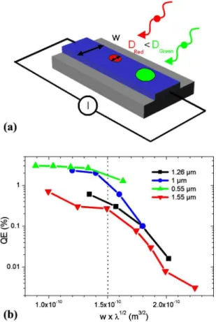
In the hot-spot model, a photon is detected only if the hot-spot is large enough, as compared to the width w of the nanowire, for the current density on the side of this hot-spot to locally overcome the critical current density, Jc关see Fig.
1共a兲兴. In a geometrical point-of-view, this condition writes
D ⬎ w共1 − I/Ic兲, 共1兲
where D is the hot-spot diameter, w is the nanowire width and I the current flowing in the nanowire. Furthermore, the hot-spot surface area, D2/4, scales as the photon energy, hc / , where is the wavelength of the incoming light. The diameter of the hot-spot is proportional to 1 /
冑
. Therefore, for a given film thickness t and a given normalized bias current I / Ic, DE should exhibit a cut-off at a given value of the reduced parameter w冑
. This condition reads:w
冑
⬍ K1, 共2兲where K1is a constant.
In order to test the latter acting law of the cut-off关Eq.
共2兲兴, we fabricated NbN SSPDs with different nanowire widths共from 80 up to 480 nm兲, the nanowire being folded on a surface of 10⫻ 10 m2 with a filling factor ranging from
0.4 to 0.6 and a length from 200 to 600 m. These SSPDs are made of NbN films of thickness 4.4 nm sputtered on a R-plane sapphire substrate.16 NbN nanowires are patterned with an electron-beam lithography, which is the most critical step of the process. This fabrication process is completely described in Refs. 4and17. Various laser diodes were used for the different excitation wavelengths. All DE were mea-sured with a bias current of I = 0.96Icat T = 4.2 K, the critical density current, jc= Ic/共wt兲 being in a 3 – 7 ⫻ 10−10 A / m2
a兲Electronic mail: [email protected].
JOURNAL OF APPLIED PHYSICS 107, 116103共2010兲
0021-8979/2010/107共11兲/116103/3/$30.00 107, 116103-1 © 2010 American Institute of Physics
range. This corresponds to an optimal working point with a dark count rate for all samples around 10 counts/s. DE is defined as the ratio of the detection pulse rate over the in-coming photon flux. The latter is measured with a calibrated semiconductor power meter.
Inset of Fig. 2 shows a measurement of the DE as a function of the nanowire width for a fixed wavelength = 1.55 m. As expected, there is a specific nanowire width, that we estimate of about 130 nm, above which DE
drops rapidly. Above this threshold, the detection mechanism changes and is most likely due to thermodynamic unbinding of vortex-antivortex pairs18 or phase-slip centers gen-eration.19,20This mechanism is much less efficient so that DE decreases rapidly for wider nanowires. This observed behav-ior is very similar to what is observed when either wave-length13 or bias current11 is varied, in agreement with the prediction of the hot-spot model. In this work, we go beyond the single parameter threshold behavior by verifying the scaling law given in Eq.共2兲. Extensive DE measurements as a function of both wavelength and nanowire width were un-dertaken. Figure1 displays the variation of DE for four dif-ferent wavelengths as a function of the normalized parameter w
冑
. A unique threshold value K1= 1.5⫻ 10−10 m3/2for thewhole set of data, in agreement with Eq.共2兲, is observed. Moreover, the diameter of the hot-spot can be easily cal-culated within this hot-spot framework. The critical nanowire width wcat a given wavelength gives the hot-spot diameter by a combination of Eqs. 共1兲 and 共2兲: D共兲 = wc共1 − I / Ic兲. This is shown in Fig.2.
The validity of the hot-spot model can be further tested in the multiphoton detection regime. Indeed, above this threshold, the energy of a single photon is not enough to trigger a resistive transition of the detector. In order to be-come resistive, the nanowire should be hit by more than one photon: this is the multiphoton regime. More precisely, it is possible to know in which regime the detector is by measur-ing the slope of the DE versus light power plot.1,21 For a mean number of m photons per pulse, the probability P共n兲 of absorbing n photons from a given pulse is given by the Pois-son distribution. For very weak 共m Ⰶ 1兲 photon fluxes, the probability of detecting one photon, two photons, and three photons is P共1兲 ⬇ m, P共2兲 ⬇m 2 2 , P共3兲 ⬇ m3 6 ,etc.
Figure3 shows the dependence of counts per second versus light power for single, two, and three-photon regime. Since the expected curve scales as Pn, where P is the incoming light power and n the number of photons needed for detec-tion, the curve slope is a direct indication of the number of photons needed to trigger a detection. We have performed FIG. 2. Hot spot diameter D for a single photon of wavelength . This
diameter is obtained from the largest nanowire width that gives a measur-able voltage pulse under a given bias current关cf. Eq.共1兲兴. The line is K1/冑
with K1being the constant extracted from the data shown in Fig.1. Inset is
an example of the determination of the minimum nanowire width
wc共⬇130 nm here兲 for detection at a wavelength = 1.55m. Dotted lines
are guides to the eye.
FIG. 1.共Color online兲 共a兲 Scheme of the hot-spot. The NbN stripe is in blue 共b兲 Dependence of normalized DE vs reduced parameter w冑at different wavelengths. This was measured with 10⫻ 10 m2 SSPDs with width
varying from 120 to 220 nm. 104 103 102 101 100 10-1 10-2 10-3 10-2 10-1 100 ~P3 ~P1 ~P2 Normalized CPS (cps/cps max )
Average photon number per pulse
FIG. 3. 共Color online兲 Dependence of normalized counts per second vs incoming light power. Circles共black兲, triangles 共red兲 and diamond 共green兲 symbols, respectively, correspond respectively to a linear, quadratic共⬀P2兲
and cubic共⬀P3兲 dependence and thus to single, two, and three-photon
re-gime because the counts per seconds are proportional to Pn, where P is the
light power and n the number of photons detected.
116103-2 Maingault et al. J. Appl. Phys. 107, 116103 共2010兲
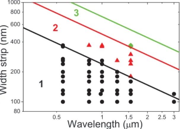
such power dependency plots for all possible 共w , 兲 values. The result is shown in Fig.4. Different regions can be clearly identified and correspond to n = 1, 2, or 3 photon regimes. The border between the n = i, n = i + 1 regions are w
冑
= Ki⬘
curves, where Ki⬘
is a constant. As the nanowire width or the photon wavelength increases the relative size of the hot-spot with respect to the nanowire width becomes too small to allow for single photon detection: one enters the two, and then three-photon regimes 共cf. Fig. 4兲. In the two-photon regime, Eq. 共1兲 becomes 2D ⬎ w共1 − I / Ic兲. This corresponds to K2⬘
= 2K1⬘
, which indicates that for a given wavelength thetwo-photon regime cut-off occurs for a nanowire width twice as large as for the single photon cut-off. We also point out that a decent fit is obtained for a value K1
⬘
= 2.0 ⫻10−10 m3/2, close to the value K1obtained from Fig.1.DE共w , 兲 scaling experiments in the single photon and multiphoton regimes have both shown a similar threshold: K1⬇ K1
⬘
. This experimental value is compared below to theexpected value obtained in the framework of the hot-spot model. We assume that when the normal area is formed, nonequilibrium quasiparticles created after the photon ab-sorption are trapped in due to the normal-superconducting interface. The number of quasiparticles can be estimated as NQPth = hc /共⑀兲, where the characteristic energy of quasiparti-cles, ⑀, is about kBTc共with kB, the Boltzmann constant and Tc, the critical temperature of the nanowire兲. On the other hand, when the superconducting gap inside the spot is sup-pressed, the quasiparticle concentration is N0kBTc, where N0
is the density of states at Fermi level. So the theoretical hot-spot volume is V = NQPth /共N0kBT兲 = hc / 共N0k
B
2
Tc2兲. Com-paring this value with the threshold diameter D = w共1 − I / Ic兲, we come to the following threshold value:
w
冑
= 2 共1 − I/Ic兲冑
hc N0kB 2 Tc2twith t the film thickness. Substituting our NbN films param-eters 共Tc= 12.3 K, N0= 1.2⫻ 1047 m−3J−1, t = 4.4 nm兲, we
obtain K1
th
= 3.1⫻ 10−9 m3/2. This value is higher than what we obtained experimentally. This may be attributed to energy and quasiparticle losses during the hot-spot formation. Quan-titatively, an internal efficiency of quasiparticles creation,,
can be determined as = NQPmeas/NQPth = 0.5%. The quality of our films and/or lithography could be one of the reasons of this poor efficiency.
In conclusion we have checked experimentally that the hot-spot picture gives a good qualitative description of the SSPD detection mechanism. When measuring SSPD effi-ciencies with different nanowire widths, we found a thresh-old well explained by the hot-spot model. The DE drops quickly when w
冑
⬎2.0⫻ 10−10 m3/2. Efficient IR detectors will therefore require narrow nanowires and their fabrication will be technologically very demanding. Our result sets the minimum nanowire width limit for designing single photon detectors in the far IR range.This work was supported by European projects FP6
STREP “SINPHONIA” 共Contract No.
NMP4-CT-2005-16433兲 and IP “QAP” 共Contract No. 15848兲.
1
G. N. Gol’tsman, O. Okunev, G. Chulkova, A. Lipatov, A. Semenov, K. Smirnov, B. Voronov, A. Dzardanov, C. Williams, and R. Sobolewski,
Appl. Phys. Lett.79, 705共2001兲.
2
D. Renker and E. Lorenz,J. Instrumentation4, P04004共2009兲.
3
K. M. Rosfjord, J. K. W. Yang, E. A. Dauler, A. J. Kerman, V. Anant, B. M. Voronov, G. N. Gol’tsman, and K. K. Berggren,Opt. Express14, 527
共2006兲.
4
R. E. de Lamaestre, L. Maingault, L. Frey, C. Constancias, P. Cavalier, J. C. Villegier, P. Odier, and J. P. Poizat,Proc. SPIE7249, 72490Q共2009兲.
5
E. F. C. Driessen and M. J. A. de Dood,Appl. Phys. Lett.94, 171109
共2009兲.
6
M. Tarkhov, J. Claudon, J. P. Poizat, A. Korneev, A. Divochiy, O. Mi-naeva, V. Seleznev, N. Kaurova, B. Voronov, A. V. Semenov, and G. Gol’tsman,Appl. Phys. Lett.92, 241112共2008兲.
7
A. Divochiy, F. Marsili, D. Bitauld, A. Gaggero, R. Leoni, F. Mattioli, A. Korneev, V. Seleznev, N. Kaurova, O. Minaeva, G. Gol’tsman, K. Lagoudakis, M. Benkhaoul, F. Levy, and A. Fiore,Nat. Photonics2, 302
共2008兲.
8
H. Takesue, S. W. Nam, Q. Zhang, R. H. Hadfield, T. Honjo, K. Tamaki, and Y. Yamamoto,Nat. Photonics1, 343共2007兲.
9
M. Halder, A. Beveratos, N. Gisin, V. Scarani, C. Simon, and H. Zbinden,
Nat. Phys.3, 692共2007兲.
10
E. le Coarer, S. Blaize, P. Benech, I. Stefanon, A. Morand, G. Lerondel, G. Leblond, P. Kern, J. M. Fedeli, and P. Royer,Nat. Photonics1, 473共2007兲.
11
A. Verevkin, J. Zhang, R. Sobolewski, A. Lipatov, O. Okunev, G. Chulkova, A. Korneev, K. Smirnov, G. N. Gol’tsman, and A. Semenov,
Appl. Phys. Lett.80, 4687共2002兲.
12
A. D. Semenov, G. N. Gol’tsman, and A. A. Korneev,Physica C351, 349
共2001兲.
13
A. Semenov, A. Engel, H.-W. Hübers, K. Il’in, and M. Siegel,Eur. Phys.
J. B47, 495共2005兲.
14
P. Haas, A. Semenov, H.-W. Hübers, J. Beyer, A. Kirste, T. Schurig, K. Il’in, M. Siegel, A. Engel, and A. Smirnov,IEEE Trans. Appl. Supercond.
17, 298共2007兲.
15
A. Semenov, A. Engel, K. Il’in, G. Gol’tsman, M. Siegel, and H.-W. Hübers,Eur. Phys. J. Appl. Phys.21, 171共2003兲.
16
J.-C. Villégier, S. Bouat, P. Cavalier, R. Setzu, R. E. de Lamaëstre, C. Jorel, P. Odier, B. Guillet, L. Mechin, M.-P. Chauvat, and P. Ruterana,
IEEE Trans. Appl. Supercond.19, 3375共2009兲.
17
C. Constancias, R. E. de Lamaëstre, O. Louveau, P. Cavalier, and J.-C. Villégier,J. Vac. Sci. Technol.25, 2041共2007兲.
18
A. D. Semenov, P. Haas, B. Günther, H.-W. Hübers, K. Il’in, M. Siegel, A. Kirste, J. Beyer, D. Drung, T. Schurig, and A. Smirnov,Supercond. Sci. Technol.20, 919共2007兲.
19
J. Kitaygorsky, J. Zhang, A. Verevkin, A. Sergeev, A. Korneev, V. Matvienko, P. Kouminov, K. Smirnov, B. Voronov, G. Gol’tsman, and R. Sobolewski,IEEE Trans. Appl. Supercond.15, 545共2005兲.
20
F. S. Jelila, J.-P. Maneval, F.-R. Ladan, F. Chibane, A. Marie-de Ficquelmont, L. Méchin, J.-C. Villégier, M. Aprili, and J. Lesueur,Phys. Rev. Lett.81, 1933共1998兲.
21
R. Sobolewski, A. Verevkin, G. Gol’tsman, A. Lipatov, and K. Wilsher,
IEEE Trans. Appl. Supercond.13, 1151共2003兲.
0.5 1 1.5 2 2 .5 3 80 10 0 20 0 40 0 60 0 80 0 1 00 0 3 1 W i d t h s t r i p ( n m ) W a v e le n g th ( m ) 2
FIG. 4. 共Color online兲 Photon regime dependence with wavelength and nanowire width. Black circles correspond to single-photon regime, red tri-angles to two-photon regime and green diamonds to three-photon regime. Lines are the expected borderlines from a regime to another, with a共⫺1/2兲 slope.
116103-3 Maingault et al. J. Appl. Phys. 107, 116103 共2010兲