Accelerating Post-Quantum Cryptography using
an Energy-Efficient TLS Crypto-Processor
The MIT Faculty has made this article openly available.
Please share
how this access benefits you. Your story matters.
Citation
Banerjee, Utsav et al. "Accelerating Post-Quantum Cryptography
using an Energy-Efficient TLS Crypto-Processor." IEEE International
Symposium on Circuits and Systems (ISCAS), October 2020, Sevilla,
Spain, Institute of Electrical and Electronics Engineers (IEEE),
October 2020. © 2020 IEEE
As Published
http://dx.doi.org/10.1109/iscas45731.2020.9180550
Publisher
Institute of Electrical and Electronics Engineers (IEEE)
Version
Author's final manuscript
Citable link
https://hdl.handle.net/1721.1/128546
Terms of Use
Creative Commons Attribution-Noncommercial-Share Alike
Accelerating Post-Quantum Cryptography using an
Energy-Efficient TLS Crypto-Processor
Utsav Banerjee
∗, Siddharth Das
†and Anantha P. Chandrakasan
∗∗Massachusetts Institute of Technology, Cambridge, MA, USA †Indian Institute of Technology Kharagpur, WB, India
Abstract—Post-quantum cryptography (PQC) is currently a growing area of research and NIST PQC Round 2/3 schemes are being actively analyzed and optimized for both security and efficiency. In this work, we re-purpose the cryptographic accelerators in an energy-efficient pre-quantum TLS crypto-processor to implement post-quantum key encapsulation schemes SIKE, Kyber, Frodo and ThreeBears and signature scheme SPHINCS+through software-hardware co-design. We utilize the modular arithmetic unit inside the elliptic curve cryptography accelerator to implement SIKE, while we use the AES and SHA2 hardware primitives to substitute SHA3 computations and accelerate the other three protocols. We accelerate the most computationally expensive components of these PQC protocols in hardware, thereby achieving up to an order of magnitude improvement in energy-efficiency over software implementations.
I. INTRODUCTION
Today’s public key cryptography protocols, such as RSA and elliptic curve cryptography (ECC), rely on the hardness of factoring and discrete logarithms for their security guar-antees. However, large-scale quantum computers can break their security by using Shor’s algorithm [1]. Recent advances in quantum computing technology have motivated a growing effort to develop new quantum-resistant public key encryption, key encapsulation and signature algorithms. Since 2016, NIST has been working on standardizing post-quantum cryptography (PQC) [2]. Detailed benchmarks of assembly-optimized ARM Cortex-M4 software implementations of the NIST Round 2/3 PQC candidates [3], [4] are available in [5].
Apart from embedded software implementations, several hardware accelerators for post-quantum cryptography have also been proposed in recent literature [6], [7], [8], [9]. However, there has been little work in exploring how existing pre-quantum RSA / ECC co-processors can be used to ac-celerate post-quantum algorithms (although not as efficiently as dedicated PQC accelerators). Recently, [10] re-purposed an RSA co-processor to accelerate polynomial multiplication in the lattice-based Kyber key encapsulation scheme.
In this work, we implement several PQC algorithms through software-hardware co-design using the energy-efficient AES, SHA2 and ECC cryptographic accelerators in a custom chip [11], [12] which we had originally designed to accelerate the TLS (Transport Layer Security) protocol. Section II provides an overview of the system architecture. In Section III, we de-scribe our implementation of isogeny-based key encapsulation SIKE[13], where we utilize the modular arithmetic unit inside the ECC accelerator to speed up isogeny computations. In Section IV, we discuss how lattice-based key encapsulation
Kyber[14], Frodo [15] and ThreeBears [16] and hash-based signature SPHINCS+ [17] are accelerated using the
AES and SHA2 accelerators. In all cases, the most com-putationally expensive functions are accelerated in hardware, achieving up to an order of magnitude improvement in energy-efficiency over software implementations.
II. TLS CRYPTO-PROCESSORARCHITECTURE
A. System Overview
The system architecture is shown in Fig. 1, along with our test chip prototype [11], [12] fabricated in 65nm CMOS process. The cryptographic accelerator consists of dedicated hardware for AES-128/256, SHA2-256 and 256-bit prime-field ECC, along with 2 KB memory, control logic and a TLS state machine. To provide more flexibility, the accelerator is coupled with a 34k-gate low-power RISC-V micro-processor [18] with Dhrystone performance comparable to ARM Cortex-M0 [19]. Our test chip operates at 16 MHz when powered at 0.8 V.
The inputs and outputs of cryptographic primitives are accessed through the accelerator memory, and a 32-bit instruc-tion register is used to program the accelerator, as shown in Fig. 1. Reads and writes to this memory take 2 cycles each. Encryption using AES-128 and AES-256 take 17 cycles and 21 cycles respectively. Initializing and loading the SHA2-256 in-ternal state both take 3 cycles, while one round of state update takes 71 cycles. These cycle counts include data movement between the accelerator memory and the cryptographic cores.
Fig. 1. System architecture and chip micrograph [11], [12], along with relevant sections of accelerator memory and cryptographic instructions.
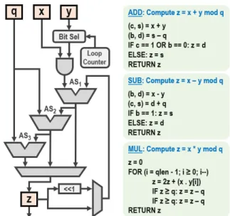
Fig. 2. Architecture for modular addition, subtraction and multiplication with configurable prime modulus q of length qlen up to 256 bits. The symbols s, c, d, b in ADD and SUB denote sum, carry, difference, borrow respectively.
Area occupied by the AES-128/256 and SHA2-256 cores are 12.6k and 18.2k logic gates respectively.
B. Modular Arithmetic Unit
While the ECC accelerator is used to execute public key cryptography algorithms, its core modular arithmetic unit can be accessed standalone to perform prime field addition (ADD), subtraction (SUB) and multiplication (MUL), as shown in Fig. 2. The registers x, y, z and q correspond to the inputs, output and prime modulus respectively. The modulus and its length qlen (≤ 256) are both configurable. The arithmetic unit consists of three adder-subtractors AS1, AS2 and AS3
which can be configured to perform addition or subtraction as required. The modular multiplication is bit-serial, with interleaved reduction. The modular addition, subtraction and multiplication algorithms, as implemented in this design, are summarized Fig. 2. Modular addition / subtraction and mul-tiplication take 9 cycles and (qlen + 11) cycles respectively, including data movement between the accelerator memory and the modular arithmetic unit. Area occupied by this circuitry is 11.8k logic gates. The ECC accelerator also consists of a 31k gate modular inverter, which is not used for the PQC algorithm implementations discussed in this work.
III. IMPLEMENTATION OFSIKE
The Supersingular Isogeny Key Encapsulation (SIKE) scheme [13] uses secret walks on isogeny graphs of super-singular elliptic curves to perform a Diffie-Hellman-like key exchange resistant to known quantum attacks. SIKE has the smallest key size among NIST Round 2 candidates, e.g., 330 byte public key and 346 byte ciphertext for SIKEp434 (un-compressed) at NIST post-quantum security level 1. However, SIKE is order of magnitude more computationally expensive than other PQC schemes [5], with 99% of the computation cost
TABLE I
PROFILING OFFpARITHMETIC INSIKEP434
FpOperation Counts S/W H/W+S/W
KeyGen Encaps Decaps Cycles Cycles fp_add 11,247 17,367 19,268 1,198 314 fp_sub 17,949 23,585 28,582 775 286 fp_neg 1 3 3 335 -fp_div2 4 8 8 608 -fp_corr 440 872 874 775 -mul 37,268 60,504 63,035 20,154 2,044 sqr 436 1,744 3,052 20,154 1,804 rdc_mont 28,952 47,072 50,420 14,457 1,470
attributed to arithmetic modulo large primes, thus motivating our use of dedicated hardware for big-integer arithmetic.
In this work, we focus on SIKEp434 which is based on the finite field Fp2, a quadratic extension of the prime field
Fp, where p = 22163137− 1 is a 434-bit prime. Since all Fp2
arithmetic can be expressed in terms of Fp, it suffices to look at
Fpoperations only. Table I summarizes the cycle counts (S/W)
of various Fp arithmetic computations and the numbers of
these operations in the KeyGen, Encaps and Decaps steps, as obtained from the publicly available optimized-C software implementation of SIKEp434 [13] profiled on our RISC-V processor. Here, fp_add, fp_sub, fp_neg, fp_div2, fp_corr, mul, sqr and rdc_mont denote modular addi-tion, subtracaddi-tion, negaaddi-tion, division by two, correction from [0, 2p) to [0, p), multiplication, squaring and Montgomery reduction respectively. Clearly, fp_add, fp_sub, mul, sqr and rdc_mont account for bulk of the computation, there-fore we optimize and accelerate these functions using the configurable modular arithmetic unit described earlier. The corresponding hardware-accelerated cycle counts (H/W+S/W) are also provided in Table I, and our implementation details are described next. Since the output of Montgomery reduction lies in [0, 2p), all these functions operate in this range [8].
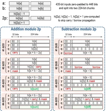
For modular addition a + b mod 2p, fp_add employs the constant-time technique of calculating a + b − 2p and then adding back 2p or 0 depending on whether a borrow was generated or not. We split each input, zero-padded to 448 bits, into two chunks (lower 224 bits in lo[·] and higher 224 bits in hi[·]) and exploit the architecture of our 256-bit modular arithmetic unit to accelerate this computation using just 4 ADD operations, as shown in Fig. 3. In the first ADD step, the modular adder’s 256-bit input registers are set to x = 0x8 · · · 0 k lo[a], y = 0x8 · · · 0 k lo[b] and q = 0x8 · · · 0 k lo[2p]. Since our modular adder always computes x + y and then subtracts q from this sum if the addition resulted in a carry (Fig. 2), setting the most significant bits of x and y to 1 ensures that we get z = carry k lo[a + b − 2p], where carry can be -1, 0 or +1. To skip explicitly calculating carry propagation for the next ADD step, we pre-compute and store hi[2p] − 1, hi[2p] and hi[2p]+1, and then set x = 0x8 · · · 0 k hi[a], y = 0x8 · · · 0 k hi[b] and q = 0x8 · · · 0 k hi[2p] − carry. The corresponding output is z = mask k hi[a + b − 2p], where mask is bit-wise AND-ed with 2p and added to a+b−2p in the final two ADD
Fig. 3. Hardware-accelerated addition and subtraction modulo 2p using our configurable 256-bit modular arithmetic unit (with its registers x, y, q, z).
steps to compute a + b mod 2p, as described in Fig. 3. Our accelerated fp_add takes 314 cycles in total.
For modular subtraction a − b mod 2p, fp_sub first calculates a − b and then adds 2p or 0 depending on whether a borrow was generated or not. We follow a technique similar to fp_add to accelerate this computation using 2 SUB and 2 ADD operations, as shown in Fig. 3, in total 284 cycles. Once again, we utilize the fact that our modular subtractor computes x − y and then adds q to this difference if the subtraction resulted in a borrow (Fig. 2). In the second SUB operation, the most significant bits of x and y are set to 0 and 1 respectively and the borrow from previous SUB step is adjusted into q to allow borrow propagation.
Although our modular multiplier computes x·y mod q, it can be used as a plain shift-and-add multiplier as long as q = 0, len(x) + len(y) ≤ 256 bits and qlen = max(len(x), len(y)). To accelerate 435-bit × 435-bit multiplication mul, we once
Fig. 4. Hardware-accelerated 224-bit × 224-bit multiplication.
again zero-pad each input to 448 bits and then split them into two 224-bit parts. Our base hardware-accelerated 224-bit × 224-bit multiplication is shown in Fig. 4. The 224-bit numbers are split further into 96 bits and 128 bits as A = A12128+ A0
and B = B12128+B0, and schoolbook multiplication A×B =
A1B12256+ (A0B1+ A1B0)2128+ A0B0 is used. Here, the
multiplications A0×B1and A1×B0are hardware-accelerated
using our 256-bit multiplier as explained earlier, while A0×B0
and A1× B1 are computed in parallel in software using the
RISC-V processor’s 32-bit ALU, which allows us to compute the final result in 490 cycles. For the 448-bit × 448-bit prod-uct, we implement Karatsuba multiplication [20]. The 448-bit inputs a and b are split into equal parts as a = a12224+ a0
and b = b12224+ b0. Then, the final 896-bit result is computed
as a × b = p22448+ p12224+ p0, where p0= a0b0, p2= a1b1
and p1= (a0+ a1)(b0+ b1) − p0− p2. Together with the three
224-bit multiplications and other additions / subtractions, our hardware-accelerated mul implementation takes 2,044 cycles, which is 10 times faster than software. For squaring sqr, we compute a × a = s22448+ s12224+ s0, where s0 = a20,
s1= 2a0a1 and s2= a21, which takes 1,804 cycles, again 11
times faster than software.
The final arithmetic function that we optimize is rdc_mont, the Montgomery reduction of the outputs of mul and sqr. All multiplications in SIKEp434 are performed in Montgomery domain [21], that is, any number a is represented as aR mod 2p with R = 2448. rdc_mont converts the product of two such numbers c = (aR)(bR) ∈ [0, 4p2) back to the Montgomery form d = (ab)R mod 2p as follows:
d = (c + (c · p0mod R) · p)/R ∈ [0, 2p)
where p0 = −p−1 mod R. Since p = 22163137 − 1 and R = 2448, this computation can be further simplified as: d = (c + (c · p0mod 2448) · 22163137− (c · p0mod 2448))/2448
= b (c + (c · p0mod 2448) · 22163137)/2448c
Fig. 5. Hardware-accelerated Montgomery reduction, where c is the 870-bit input, d is the 435-bit reduced output and ˆp = p + 1. Multiplications are shown in red, and the steps where d is calculated are shown in blue.
TABLE II
PERFORMANCE OFSIKEP434
S/W Only S/W + H/W Accel
Cycles Energy Cycles Energy
KeyGen 1,220,667,380 48.83 mJ 156,842,207 7.06 mJ Encaps 1,999,384,639 79.98 mJ 256,976,178 11.56 mJ Decaps 2,132,422,690 85.30 mJ 273,987,430 12.33 mJ
We re-structure the Comba-based Montgomery reduction al-gorithm from [22] for the 434-bit prime p and 128-bit radix so that we can use our 256-bit multiplier. The corresponding pseudo-code is shown in Fig. 5, where c, d and ˆp = p + 1 are shown as 32-bit arrays with 28, 14 and 14 elements respectively. Several multiplications are saved since the 216 least significant bits of ˆp are zeros. Once again, we perform arithmetic computations in parallel in software and in the accelerator. To efficiently interleave these computations, we re-order them as shown in Fig. 5. The modular reduction take 1,470 cycles overall, which is 10 times faster than software.
The overall cycle counts and energy consumption of SIKEp434, both software and hardware-accelerated versions, are reported in Table II. All SHA3-related functions are performed in software since they account for less than 1% of the total computation cost. With the fast arithmetic implemen-tations described earlier, we achieve ≈ 8× reduction in energy consumption compared to RISC-V software. We are able to perform key encapsulation in 16.1 s while consuming 11.56 mJ of energy (at 16 MHz and 0.8 V), which is 3× faster and 9× more energy-efficient (after accounting for supply voltage scaling) than the optimized ARM Cortex-M4 implementation from [5] (with specialized FPU and DSP instructions) having 44.4 s key encapsulation time with 1.76 J energy consumption (at 24 MHz and 3.3 V) [23]. While our implementation is much slower than dedicated SIKE hardware accelerators [8], [13], our logic area cost is significantly smaller. For example, the SIKE accelerator from [13], which performs key encapsulation in 10 ms at 350 MHz, consists of a million gates, while our modular arithmetic unit has only 11.8k-gate
area. Our proposed techniques can also be easily extended to larger SIKE parameters without any change in the hardware.
IV. IMPLEMENTATION OFOTHERPQC SCHEMES
We also explore the lattice-based CCA-secure key encapsu-lation schemes Kyber, Frodo and ThreeBears, and the hash-based signature scheme SPHINCS+ at different security levels. Unlike SIKE, a significant portion of the computation costs (70%, 70%, 50% and 95% respectively) of these pro-tocols is attributed to SHA3-based hashing and extendable output functions [5]. Although NIST has required the use of SHA3 as the symmetric primitive for PQC standardiza-tion for the sake of uniformity, PQC candidates have also proposed variants of their algorithms which use AES and SHA2 in order to benefit from widely deployed hardware accelerators, for example, Kyber-90s, Frodo-AES and SPHINCS+-SHA256. Following the same approach, we use our energy-efficient AES-128/256 and SHA2-256 hardware as a substitute for SHA3, similar to [10]. The SHA2-256 hash function is used as a drop-in replacement of SHA3-256 wherever SHA3-256-bit message digests are required. As a replacement for the SHAKE-256 extendable output func-tion which absorbs an arbitrary-length byte-string and then squeezes out a specified number of bytes, we first use SHA2-256 to compute a SHA2-256-bit digest of the input, and then generate output bytes using AES-256 in counter mode with this 256-bit digest used as the key. Similarly, SHA2-256 and AES-128 are used instead of SHAKE-128. For Kyber-90s, SHA2-512 is used to replace SHA3-512, for which the energy is estimated through simulation (using a 34.2k-gate SHA2-256/512 core) since our original chip has SHA2-256 only. Frodo-976 and Frodo-1344require more than 64 KB of data memory, so their energy are also estimated from simulation.
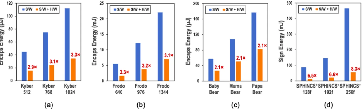
The cycle counts and energy consumption (at 16 MHz and 0.8 V) of these protocols are shown in Tables III, IV, V and VI. The energy consumption at various security levels is also shown in Figure 6 and compared with software. Clearly, using the AES and SHA2 hardware accelerators provides 2-8× improvement in energy-efficiency compared to implementing
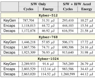
TABLE III PERFORMANCE OFKY B E R
S/W Only S/W + H/W Accel Cycles Energy Cycles Energy
Kyber-512 KeyGen 787,704 31.51 µJ 293,410 10.27 µJ Encaps 1,118,013 44.72 µJ 444,103 15.54 µJ Decaps 1,172,878 46.92 µJ 616,554 21.58 µJ Kyber-768 KeyGen 1,446,218 57.85 µJ 506,171 17.72 µJ Encaps 1,867,756 74.71 µJ 690,306 24.16 µJ Decaps 1,923,309 76.93 µJ 913,640 31.98 µJ Kyber-1024 KeyGen 2,289,933 91.6 µJ 765,289 26.79 µJ Encaps 2,803,529 112.14 µJ 983,586 34.43 µJ Decaps 2,863,020 114.52 µJ 1,260,599 44.12 µJ TABLE IV PERFORMANCE OFFR O D O S/W Only S/W + H/W Accel Cycles Energy Cycles Energy
Frodo-640 KeyGen 117,818,447 4.71 mJ 28,733,817 1.01 mJ Encaps 138,875,003 5.56 mJ 47,859,403 1.68 mJ Decaps 139,454,719 5.58 mJ 48,439,119 1.70 mJ Frodo-976 KeyGen 257,305,186 10.29 mJ 63,911,764 2.24 mJ Encaps 304,146,300 12.17 mJ 107,056,023 3.75 mJ Decaps 304,852,720 12.19 mJ 107,734,913 3.77 mJ Frodo-1344 KeyGen 465,060,396 18.6 mJ 121,686,070 4.26 mJ Encaps 551,033,493 22.04 mJ 202,610,302 7.09 mJ Decaps 552,006,180 22.08 mJ 203,582,989 7.13 mJ
SHA3 in software on the RISC-V, and is also up to an order of magnitude lower energy consumption compared to the ARM Cortex-M4 implementations from [5]. Once again, our implementations are much slower than dedicated lattice-based cryptography and hash-lattice-based signature accelerators such as [9] and [6]. For example, the configurable lattice crypto-processor from [9] contains 106k logic gates and runs at 72 MHz. In comparison, our implementation requires 30.8k (46.8k) logic gates, which is the combined area of the AES-128/256 and SHA2-256 (SHA2-256/512) hardware blocks, hence much smaller than dedicated PQC accelerators.
V. CONCLUSION ANDFUTUREWORK
This work demonstrates energy-efficient post-quantum cryp-tography accelerated using a pre-quantum TLS crypto-processor. In particular, we have implemented some of the NIST PQC Round 2 schemes where majority of the compu-tation cost is due to either big-integer arithmetic or hashing. We re-purpose the modular arithmetic unit inside the ECC accelerator to speed up isogeny-based SIKE key
encapsu-TABLE V
PERFORMANCE OFTH R E EBE A R S
S/W Only S/W + H/W Accel Cycles Energy Cycles Energy
ThreeBears-BabyBear KeyGen 1,134,969 45.40 µJ 510,168 17.86 µJ Encaps 1,435,457 57.42 µJ 768,387 26.89 µJ Decaps 2,349,906 94.00 µJ 1,289,282 45.12 µJ ThreeBears-MamaBear KeyGen 2,299,103 91.96 µJ 1,085,198 37.98 µJ Encaps 2,705,222 108.21 µJ 1,448,786 50.71 µJ Decaps 3,967,321 158.69 µJ 2,190,627 76.67 µJ ThreeBears-PapaBear KeyGen 3,901,979 156.08 µJ 1,894,745 66.32 µJ Encaps 4,416,453 176.66 µJ 2,366,458 82.83 µJ Decaps 6,035,889 241.44 µJ 3,339,675 116.89 µJ TABLE VI PERFORMANCE OFSPHINCS+ S/W Only S/W + H/W Accel
Cycles Energy Cycles Energy
SPHINCS+-128f KeyGen 70,431,613 2.82 mJ 12,404,925 0.43 mJ Sign 2,221,929,206 88.88 mJ 393,326,377 13.77 mJ Verify 96,661,677 3.87 mJ 17,097,986 0.60 mJ SPHINCS+-192f KeyGen 134,599,011 5.38 mJ 23,222,714 0.81 mJ Sign 3,664,050,463 146.56 mJ 633,698,932 22.18 mJ Verify 199,673,588 7.99 mJ 34,218,169 1.2 mJ SPHINCS+-256f KeyGen 514,669,630 20.59 mJ 70,997,594 2.48 mJ Sign 11,652,022,152 466.08 mJ 1,603,200,319 56.11 mJ Verify 300,838,369 12.03 mJ 40,530,784 1.42 mJ
lation. We also use AES and SHA2 hardware primitives to substitute SHA3 computations and accelerate lattice-based Kyber, Frodo and ThreeBears key encapsulation and hash-based SPHINCS+ signatures. Overall we achieve up
to an order of magnitude improvement in energy-efficiency compared to optimized software implementations. While PQC protocols are still being analyzed for security and efficiency, our work shows that existing embedded devices with standard cryptographic accelerators can still be used to reasonably speed up PQC implementations until new optimized PQC hardware accelerators are designed and integrated with them. Although the core hardware accelerators are orders of magni-tude more efficient than software, we were unable to achieve similar efficiency in our software-hardware co-design due to latency of the memory-mapped interface. This may possibly be addressed by using direct memory access interface, which will be explored in future work.
ACKNOWLEDGMENT
REFERENCES
[1] P. W. Shor, “Polynomial-Time Algorithms for Prime Factorization and Discrete Logarithms on a Quantum Computer,” SIAM Journal of Computing, vol. 26, no. 5, pp. 1484-1509, Oct. 1997.
[2] L. Chen et al., “Report on Post-Quantum Cryptography,” NIST Technical Report, no. 8105, Apr. 2016.
[3] G. Alagic et al., “Status Report on the First Round of the NIST Post-Quantum Cryptography Standardization Process,” NIST Technical Report, no. 8240, Jan. 2019.
[4] G. Alagic et al., “Status Report on the Second Round of the NIST Post-Quantum Cryptography Standardization Process,” NIST Technical Report, no. 8309, Jul. 2020.
[5] M. J. Kannwischer, J. Rijneveld, P. Schwabe and K. Stoffelen, “pqm4: Testing and Benchmarking NIST PQC on ARM Cortex-M4,” NIST 2nd PQC Standardization Conference, Aug. 2019.
[6] D. Amiet et al., “FPGA-based Accelerator for Post-Quantum Signature Scheme SPHINCS-256,” IACR Trans. on Cryptographic Hardware and Embedded Systems (TCHES), vol. 2018, no. 1, pp. 18-39, Feb. 2018. [7] J. Howe et al., “Standard Lattice-Based Key Encapsulation on Embedded
Devices,” IACR Trans. on Cryptographic Hardware and Embedded Systems (TCHES), vol. 2018, no. 3, pp. 372-393, Aug. 2018. [8] B. Koziel et al., “A High-Performance and Scalable Hardware
Architec-ture for Isogeny-Based Cryptography,” IEEE Trans. on Computers, vol. 67, no. 11, pp. 1594-1609, Nov. 2018.
[9] U. Banerjee, T. S. Ukyab and A. P. Chandrakasan, “Sapphire: A Configurable Crypto-Processor for Post-Quantum Lattice-based Proto-cols,” IACR Trans. on Cryptographic Hardware and Embedded Systems (TCHES), vol. 2019, no. 4, pp. 17-61, Aug. 2019.
[10] M. Albrecht et al., “Implementing RLWE-based Schemes Using an RSA Co-Processor,” IACR Trans. on Cryptographic Hardware and Embedded Systems (TCHES), vol. 2019, no. 1, pp. 169-208, Nov. 2018. [11] U. Banerjee et al., “An Energy-Efficient Reconfigurable DTLS
Crypto-graphic Engine for End-to-End Security in IoT Applications,” IEEE Int. Solid-State Circuits Conference (ISSCC), pp. 42-44, Feb. 2018. [12] U. Banerjee et al., “An Energy-Efficient Reconfigurable DTLS
Crypto-graphic Engine for Securing Internet-of-Things Applications,” in IEEE Journal of Solid-State Circuits, vol. 54, no. 8, pp. 2339-2352, Aug. 2019.
[13] D. Jao et al., “Supersingular Isogeny Key Encapsulation (SIKE) – Al-gorithm Specifications and Supporting Documentation,” NIST Technical Report, 2019.
[14] R. Avanzi et al., “CRYSTALS-Kyber – Algorithm Specifications and Supporting Documentation,” NIST Technical Report, 2019.
[15] M. Naehrig et al., “FrodoKEM: Learning With Errors Key Encapsula-tion – Algorithm SpecificaEncapsula-tions and Supporting DocumentaEncapsula-tion,” NIST Technical Report, 2019.
[16] M. Hamburg, “ThreeBears – Algorithm Specifications and Supporting Documentation,” NIST Technical Report, 2019.
[17] J.-P. Aumasson et al., “SPHINCS+ – Algorithm Specifications and Supporting Documentation,” NIST Technical Report, 2019.
[18] A. Waterman et al., “The RISC-V Instruction Set Manual Volume I: User-Level ISA Version 2.0,” Technical Report, EECS Department, University of California, Berkeley, UCB / EECS-2014-54, May 2014. [19] ARM Holdings, ARM Cortex-M Series Processors. [Online]. Available:
https://developer.arm.com/products/processors/cortex-m
[20] A. Karatsuba and Y. Ofman, “Multiplication of Many-Digital Numbers by Automatic Computers,” Proceedings of the USSR Academy of Sci-ences, vol. 145, no.2, pp. 293-294, Feb. 1962.
[21] P. L. Montgomery, “Modular Multiplication Without Trial Division,” Mathematics of Computation, vol. 44, no. 170, pp. 519-521, Apr. 1985. [22] C. Costello et al., “Efficient Algorithms for Supersingular Isogeny Diffie-Hellman,” Advances in Cryptology (CRYPTO), pp. 572-601, Aug. 2016. [23] STMicroelectronics, STM32F4 Series of High-Performance MCUs with DSP and FPU Instructions. [Online]. Available: https://www.st.com/en/microcontrollers-microprocessors/stm32f4-series.html
This is an extended version of the paper published in 2020 IEEE International Symposium on Circuits and Systems (ISCAS) - DOI: 10.1109/ISCAS45731.2020.9180550
![Fig. 1. System architecture and chip micrograph [11], [12], along with relevant sections of accelerator memory and cryptographic instructions.](https://thumb-eu.123doks.com/thumbv2/123doknet/13819738.442509/2.918.474.839.799.1030/architecture-micrograph-relevant-sections-accelerator-memory-cryptographic-instructions.webp)