1.8-μm thulium microlasers integrated on silicon
The MIT Faculty has made this article openly available.
Please share
how this access benefits you. Your story matters.
Citation
Bradley, Jonathan D. B., et al. "1.8-Μm Thulium Microlasers
Integrated on Silicon." Proceedings Volume 9744, Optical
Components and Materials XIII, 13-18 February, 2016, San
Francisco, California, edited by Shibin Jiang and Michel J. F.
Digonnet, SPIE, 2016, p. 97440U. © 2016 SPIE
As Published
http://dx.doi.org/10.1117/12.2213678
Publisher
SPIE
Version
Final published version
Citable link
http://hdl.handle.net/1721.1/116509
Terms of Use
Article is made available in accordance with the publisher's
policy and may be subject to US copyright law. Please refer to the
publisher's site for terms of use.
PROCEEDINGS OF SPIE
SPIEDigitalLibrary.org/conference-proceedings-of-spie
1.8-μm thulium microlasers
integrated on silicon
Jonathan D. B. Bradley, Zhan Su, E. Salih Magden,
Nanxi Li, Matthew Byrd, et al.
Jonathan D. B. Bradley, Zhan Su, E. Salih Magden, Nanxi Li, Matthew
Byrd, Purnawirman P., Thomas N. Adam, Gerald Leake, Douglas
Coolbaugh, Michael R. Watts, "1.8-μm thulium microlasers integrated on
silicon," Proc. SPIE 9744, Optical Components and Materials XIII, 97440U (24
February 2016); doi: 10.1117/12.2213678
1.8-µm thulium microlasers integrated on silicon
Jonathan D. B. Bradley,*
a,bZhan Su,
aE. Salih Magden,
aNanxi Li,
a,cMatthew Byrd,
aPurnawirman,
aThomas N. Adam,
dGerald Leake,
dDouglas Coolbaugh,
dMichael R. Watts
aa
Research Laboratory of Electronics, Massachusetts Institute of Technology, 77 Massachusetts
Avenue, Cambridge, Massachusetts 02139, USA;
b
Current address: Department of Engineering Physics, McMaster University, 1280 Main Street
West, Hamilton, Ontario L8S 4L7, Canada;
c
John A. Paulson School of Engineering and Applied Sciences, Harvard University, 29 Oxford
Street, Cambridge, Massachusetts, 02138, USA;
d
College of Nanoscale Science and Engineering, State University of New York, 257 Fuller Road,
Albany, New York 12203, USA
ABSTRACT
A key challenge for silicon photonic systems is the development of compact on-chip light sources. Thulium-doped fiber and waveguide lasers have recently generated interest for their highly efficient emission around 1.8 µm, a wavelength range also of growing interest to silicon-chip based systems. Here, we report on highly compact and low-threshold thulium-doped microcavity lasers integrated with silicon-compatible silicon nitride bus waveguides. The 200-µm-diameter thulium microlasers are enabled by a novel high quality-factor (Q-factor) design, which includes two silicon nitride layers and a silicon dioxide trench filled with thulium-doped aluminum oxide. Similar, passive (undoped) microcavity structures exhibit Q-factors as high as 5.7 × 10⁵ at 1550 nm. We show lasing around 1.8–1.9 µm in
aluminum oxide microcavities doped with 2.5 × 1020 cm−3 thulium concentration and under resonant pumping around 1.6
µm. At optimized microcavity-waveguide gap, we observe laser thresholds as low as 773 µW and slope efficiencies as high as 23.5%. The entire fabrication process, including back-end deposition of the gain medium, is silicon-compatible and allows for co-integration with other silicon-based photonic devices for applications such as communications and sensing.
Keywords: Thulium, lasers, silicon photonics, integrated optics, microcavities, rare-earth-ion-doped devices
1. INTRODUCTION
Rare-earth-ion-doped integrated lasers offer distinct advantages compared to the alternative approaches used to fabricate lasers on silicon [1]. They are monolithic, low cost, and use straightforward fabrication methods, enabling wafer-scale processing. In addition, they provide lasing in multiple technologically important wavelength bands (e.g. ytterbium at 1.0 µm, neodymium at 1.3 µm, and erbium at 1.5 µm), have low thermal sensitivity, and can provide high output power, narrow linewidth and wavelength tunability. Using a single low-cost pump source to excite multiple rare earth lasers can mitigate the requirement for optical pumping. Indeed, the realization of low-threshold integrated microcavity lasers [2] demonstrates the potential to power multiple lasers on the same chip with minimal power consumption. Recent work has led to methods for fabricating erbium- and ytterbium-doped lasers using CMOS-compatible silicon nitride cavities [3–5], enabling integration of such lasers in silicon electronic-photonic microsystems.
Thulium lasers have attracted much interest of late for their high efficiencies and eye-safe emission in the wavelength range from 1.7–2.2 µm [6–8]. They have been developed in various platforms, including fibers, bulk crystals, planar and channel waveguides and have important applications in gas sensing, free space communications, biomedicine and nonlinear mid-infrared generation. Nevertheless, thulium lasers integrated on silicon are relatively unexplored. The recent investigation of silicon microsystems at longer wavelengths [9] and a prospective communication window near 2 µm [10], as well as other emerging applications, provide strong motivations for developing thulium lasers on a silicon platform.
*email: [email protected]; phone: 1-905-525-9140 ext. 24013; engphys.mcmaster.ca
Optical Components and Materials XIII, edited by Shibin Jiang, Michel J. F. Digonnet, Proc. of SPIE Vol. 9744, 97440U · © 2016 SPIE · CCC code: 0277-786X/16/$18
doi: 10.1117/12.2213678 Proc. of SPIE Vol. 9744 97440U-1
a)
Pump<-Sputtering guns (RF power supplies) Ar inletb)
M 8
E U O2 inlet Substrate holder & heaterï
'-' 4) V2 C oU
H 0 0 13 -0,
10 15 20 25 Tm Power (W)In this paper we report on low-threshold thulium-doped microcavity lasers integrated on a silicon chip. We fabricate the microlasers using a silicon-compatible process which includes an integrated silicon nitride waveguide for coupling both pump and laser light to and from the microcavity and a thulium-doped aluminum oxide (Al2O3:Tm3+) gain layer
deposited as a back-end step. We show lasing in the range 1.8–1.9 µm by varying the microcavity-waveguide gap, a threshold as low as 773 µW, and slope efficiency as high as 23.5% vs. on-chip pump power.
2. FABRICATION
2.1 Al2O3:Tm3+ Deposition
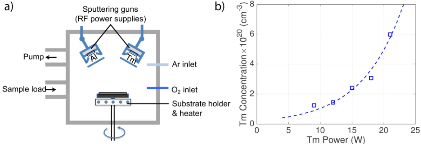
We deposited Al2O3:Tm3+ films onto thermally oxidized silicon substrates using a process similar to that described in
[11]. The doped films were reactively co-sputtered from metallic aluminum and thulium targets in an oxygen and argon atmosphere. The deposition system, which is equipped with two radio frequency (RF) magnetron sputtering guns, is shown in Fig. 1a. We operated the aluminum sputtering gun at a power of 200 W and carried out the deposition at a pressure of 3 mTorr. The argon flow rate was held at 11 sccm, while the oxygen flow was adjusted between 1.0 to 1.5 sccm in order to maintain the oxygen flow-bias voltage curve at the “knee” point of the hysteresis curve [12]. At this point the films are stoichiometric, while the oxygen flow is maintained below the point where the aluminum target becomes poisoned and the bias voltage and deposition rate drop precipitously. During deposition, we set the substrate temperature to 500 °C in order to obtain lowest film losses. We determined the Tm concentration in the films using Rutherford backscattering spectrometry (RBS). As shown in Fig. 1b, we obtain Tm concentrations between 1 and 6 × 1020 cm−3 by adjusting Tm sputtering powers in the range 9-21 W. Using a prism coupling system, we measured the
propagation loss in the films at 633 nm (outside the Tm absorption) and determined background losses of ≤ 0.1 dB/cm.
Figure 1. a) Illustration of deposition system used for reactive magnetron co-sputtering of Al2O3:Tm3+ films; b) Tm concentration vs. sputtering power as measured by Rutherford backscattering spectrometry (Al sputtering power = 200 W, the line is an exponential fit and serves as a guide to the eye).
2.2 Microcavity Design and Fabrication
We fabricated the microcavity lasers on silicon chips using a 300-mm CMOS foundry with a 65-nm technology node. The design is similar to that reported for erbium- and ytterbium-doped microcavity lasers in [5]. First, we deposited a 6-µm-thick plasma-enhanced chemical vapor deposition (PECVD) SiO2 bottom cladding layer on a 300-mm silicon wafer,
followed by deposition and patterning of two 200-nm-thick PECVD Si3N4 layers with a 100-nm-thick SiO2 layer in
between. We patterned both Si3N4 layers using 193-nm immersion lithography and reactive ion etching, yielding Si3N4
waveguide widths of 0.9 µm (designed for phase-matched 1.6-µm pumping) and microcavity-waveguide gaps ranging from 0.2 to 1.3 µm (in 0.1 µm steps). We deposited a 4-µm-thick SiO2 layer over the top, then patterned and etched
4-µm-deep microcavity trenches (outer diameter = 200 µm) using the upper Si3N4 layer as an etch stop. After removal of
the Si3N4 top layer (except for the top part of the waveguide and residual pieces at the edge of the microcavity), we
b) Si in Si3N4 SiO2 AI203:Tm3+ microcavity
(0 = 200 pm)
gar p waveguide Pump Laser (1.6 µm) Pol. Controller Pump Signal Tm Microlasero
for dicing and fiber end-coupling, transferred the wafers from the silicon foundry and diced the wafers into individual dies. We loaded several dies into the sputtering chamber and deposited a 1.5-µm-thick Al2O3:Tm3+ film on top. A
thinner layer was deposited on the cavity sidewalls due to the angle of the sputtering guns. For this work we selected a sputtering power of 15 W and thulium concentration of 2.5 × 1020 cm-3 – high enough to achieve greater gain than cavity
losses, but low enough to maintain low threshold lasing (determined based on a Q-factor of up to 5.7 x 10⁵ obtained at
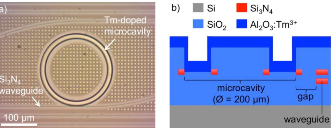
1550 nm in [5]). We show an optical microscope image of the fabricated thulium microlaser in Fig. 2a and a cross-section drawing of the microcavity in Fig. 2b.
Figure 2. a) Optical microscope image of a Tm-doped microcavity laser and b) cross-section drawing showing the microcavity design.
3. EXPERIMENTAL SETUP
We characterized the microcavity lasers using the experimental setup shown in Fig. 3. We coupled pump light from a 1.6-µm tunable laser (100 kHz linewidth) to the chip via a polarization controller, fiber wavelength division multiplexor (WDM), and tapered optical fiber. The laser output was also coupled from the chip using tapered optical fibers on both sides, filtered from the pump light with WDMs and coupled to optical spectrum analyzers (OSAs) to observe the output spectra and power. The transmitted pump light was measured using a power meter.
Figure 3. Experimental setup used to characterize the thulium-doped microcavity lasers.
4. RESULTS
We measured the transmission properties of the Al2O3:Tm3+ films and microcavities around the pump wavelength. In
Fig. 4a we show the Al2O3:Tm3+ film absorption, measured by prism coupling. We observe peak Tm3+ ion absorption >
1.6 µm as observed in other host materials [6–8] (we note that the measurement upper limit was determined by the
ion (dB/cm) a,
1
N U1 N Ul CO fission (dB) --P No
Q 0.5 0 1500 1550 1600 1650 -10 1595 1600 1605 1610 1615 Wavelength (nm) Wavelength (nm) 300 ._ 7o vs. on -chip pump power vs. ahsnrh.d numn flower a) 200
/
A
v
) 15,z7
I V
-5 50_.,/ _,,,,,
500 1000 1500 Pump Power (µW) 2000maximum wavelength of the tunable laser – 1.64 µm). The transmitted pump power for a device with microcavity-waveguide gap of 0.9 µm and transverse magnetic (TM) polarization is shown in Fig. 4b. We observe three resonances (marked by red arrows) corresponding to different microcavity modes of different azimuthal orders, with the lasing resonance indicated by a red circle (i.e. the resonance with most of the light intensity propagating in the Al2O3:Tm3+ gain
medium).
Figure 4. a) Absorption spectrum in a Al2O3:Tm3+ film around 1.6 µm showing peak absorption > 1.6 µm. b) Transmission measurement in thulium-doped microcavity with microcavity-waveguide gap of 0.9 µm under TM polarization around 1.6 µm (lasing resonance indicated by red circle).
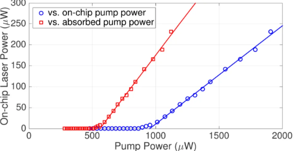
We observed the highest laser efficiency for the device with gap 0.9 µm. Fig. 5 shows the double-sided laser output power measured as a function of on-chip and absorbed pump power. The on-chip power is the power coupled into the silicon nitride waveguide, taking into account the fiber-chip coupling loss of ~3 dB, and the absorbed power is the power coupled into the microcavity. We observe efficiencies of 23.5 and 40%, respectively. We observe the lowest device threshold of 773 µW vs. on-chip pump power at a gap of 1.0 µm.
Figure 5. Laser curves under resonant 1608-nm pumping for a microcavity with gap 0.9 µm.
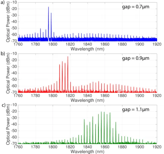
In Figs. 6a–c we show the laser spectra obtained under 1608-nm pumping and at different gaps. We observe multimode lasing over a span of ~100 nm, ranging from 1.8–1.9 µm. At smaller gaps we observe lasing at shorter wavelengths where the gain is higher and can compensate for the reduced loaded Q-factor of the cavity. Likewise, at larger gaps, where the loaded Q-factor of the cavity is higher, we observe lasing at longer wavelengths where Tm3+ absorption, gain
a) co -20 -30 g -40 o_ -50 -60
gap = 0.7pm
ILLi.,11.11,111111LLI.111.1.11.11.1_ O -70 1760 b) -L---10 -20i-30
-30i-40
1780 1800 1820 1840 1860 Wavelength (nm) 1880 1900 1920gap = 0.9pm
- -50
c
}i2
,-60 Q O -70 1760 c)---10 -20 1780 1800 1820 1840 1860 Wavelength (nm) 1880 1900 1920 gap = 1.1 pm m -30 ó -40 -50 as 60 -Q O -70 1760 1780 1800 1820 1840 1860 Wavelength (nm) 1880 1900 1920Figure 6. Laser emission spectra under 1608-nm pumping and at microcavity-waveguide gaps of a) 0.7 µm, b) 0.9 µm and c) 1.1 µm.
5. CONCLUSION
In summary, we have demonstrated low-threshold thulium-doped microcavity lasers on silicon. The microcavity devices are integrated with silicon nitride waveguides for coupling pump light into the cavity and laser output on the chip. We measure sub-milliwatt thesholds with respect to power coupled into the silicon nitride waveguide and obtain slope efficiencies of up to 23.5 and 40% vs. on-chip and absorbed pump power, respectively. These results show that thulium lasers are of significant interest for silicon photonic microsystems applications near 2 µm.
ACKNOWLEDGEMENTS
This work is supported by the Defense Advanced Research Projects Agency (DARPA) Microsystems Technology Office’s (MTO) DODOS (HR0011-15-C-0056) and E-PHI (HR0011-12-2-0007) projects. N. Li acknowledges a fellowship from the Agency of Science, Technology and Research (A*STAR), Singapore.
REFERENCES
[1] Bradley, J. D. B. and Pollnau, M., “Erbium-doped integrated waveguide amplifiers and lasers,” Laser Photonics Rev. 5(3), 368-403 (2011).
[2] Polman, A., Min, B., Kalkman, J., Kippenberg, T. J. and Vahala, K. J., “Ultralow-threshold erbium-implanted toroidal microlaser on silicon,” Appl. Phys. Lett. 84(7), 1037-1039 (2004).
[3] Purnawirman, Sun, J., Adam, T. N., Leake, G., Coolbaugh, D., Bradley, J. D. B., Shah Hosseini, E. and Watts, M. R., “C- and L-band erbium-doped waveguide lasers with wafer-scale silicon nitride cavities,” Opt. Lett. 38(11), 1760-1762 (2013).
[4] Belt, M., Huffman, T., Davenport, M. L, Li, W., Barton, J. S. and Blumenthal, D. J., “Arrayed narrow linewidth erbium-doped waveguide-distributed feedback lasers on an ultra-low-loss silicon-nitride platform,” Opt. Lett. 38(22), 4825-4828 (2013).
[5] Bradley, J. D. B., Shah Hosseini, E., Purnawirman, Su, Z., Adam, T. N., Leake, G., Coolbaugh, D. and Watts, M. R., “Monolithic erbium- and ytterbium-doped microring lasers on silicon chips,” Opt. Express 22(10), 12226-12237 (2014).
[6] Wang, Q., Geng, J. and Jiang, S., “2-µm fiber laser sources for sensing,” Opt. Eng. 53(6), 061609 (2014).
[7] Scholle, K., Lamrini, S., Koopmann, P. and Fuhrberg, P., [Frontiers in Guided Wave Optics and Optoelectronics], In Tech, India, 471-500 (2010).
[8] Huber, G., Kränkel, C. and Petermann, K., “Solid-state lasers: status and future,” J. Opt. Soc. Am. B 27(11), B93-B105 (2010).
[9] Roelkens, G., Dave, U. D., Gassenq, A., Hattasan, N., Hu, C., Kuyken, B., Leo, F., Malik, A., Muneeb, M., Ryckeboer, E., Sanchez, D., Uvin, S., Wang, R., Hens, Z., Baets, R., Shimura, Y., Gencarelli, F., Vincent, B., Loo, R., Van Campenhout, J., Cerutti, L., Rodriguez, J.-B., Tournié, E., Chen, X., Nedeljkovic, M., Mashanovich, G., Shen, L., Healy, N., Peacock, A. C., Liu, X., Osgood, R. and Green, W. M. J., “Silicon-based photonic integration beyond the telecommunication wavelength range,” IEEE J. Sel. Top. Quantum Electron. 20(4), 8201511 (2014). [10] Ackert, J. J., Thomson, D. J., Shen, L., Peacock, A. C., Jessop, P. E., Reed, G. T., Mashanovich, G. Z. and Knights,
A. P., “High-speed detection at two micrometres with monolithic silicon photodiodes,” Nat. Photon. 9(6), 393-397 (2015).
[11] Wörhoff, K., Bradley, J. D. B., Ay, F., Geskus, D., Blauwendraat, T. P. and Pollnau, M., “Reliable low-cost fabrication of low-loss Al2O3:Er3+ waveguides with 5.4-dB optical gain,” IEEE J. Quantum Electron. 45(5), 454-461
(2009).
[12] Koski, K., Hölsä, J. and Juliet, P., “Voltage controlled reactive sputtering process for aluminum oxide thin films,” Thin Solid Films 326(1-2), 189-193 (1998).