HAL Id: hal-00166373
https://hal.archives-ouvertes.fr/hal-00166373
Submitted on 5 Aug 2007
HAL is a multi-disciplinary open access
archive for the deposit and dissemination of
sci-entific research documents, whether they are
pub-lished or not. The documents may come from
teaching and research institutions in France or
abroad, or from public or private research centers.
L’archive ouverte pluridisciplinaire HAL, est
destinée au dépôt et à la diffusion de documents
scientifiques de niveau recherche, publiés ou non,
émanant des établissements d’enseignement et de
recherche français ou étrangers, des laboratoires
publics ou privés.
How to Implement an Asynchronous Test Wrapper for
Network-on-Chip Nodes
Xuan Tu Tran, Jean Durupt, François Bertrand, Vincent Beroulle, Chantal
Robach
To cite this version:
Xuan Tu Tran, Jean Durupt, François Bertrand, Vincent Beroulle, Chantal Robach. How to
Imple-ment an Asynchronous Test Wrapper for Network-on-Chip Nodes. The 12th IEEE European Test
Symposium (ETS 2007), May 2007, Freiburg, Germany. pp.Tran07HTI. �hal-00166373�
How to Implement an Asynchronous Test Wrapper for Networks-on-Chip Nodes
Xuan-Tu Tran, Jean Durupt, Franc¸ois Bertrand CEA-LETI, Minatec
17 rue des Martyrs, 38054 Grenoble, France [email protected]
Vincent Beroulle, Chantal Robach INPG-LCIS
50 rue Barth´el´emy de Laffemas, Valence, France [email protected]
Abstract
The Network-on-Chip (NoC) paradigm is currently known as an alternative solution for the on chip communication in the next SoC generation, especially, asynchronous NoCs. One of the challenges for asynchronous NoC-based systems design is testing asynchronous network architectures for manufactur-ing defects. To improve the testability of asynchronous NoCs, we have developed a scalable and configurable asynchronous Design-for-Test (DfT) architecture. In this architecture, each asynchronous network node is surrounded by an asynchronous test wrapper and the network communication channels are reused as a high-speed Test Access Mechanism (TAM). This architecture is designed to test all network elements (routers, communication channels), but it can also be used to test com-putational resources. In this paper, we introduce how to real-ize and implement the test wrapper in Quasi Delay Insensitive (QDI) asynchronous logic style. The validation and experi-mental results are also presented.
1. Introduction
In large complex Systems-on-Chip (SoCs), classical inter-connect architectures (point-to-point, bus, or bus-hierarchy) cannot meet the needs of on-chip communication because of many disadvantages: long wire loads and resistances, crosstalk, shared bandwidth, scalability, etc. Networks-on-Chip (NoCs) have recently emerged as an alternative solution for the on chip communication of large complex SoCs. The advantages of NoC-based systems are numerous: high scala-bility and versatility, high throughput communication, as well as good power efficiency [4, 5, 7].
Despite having many attractive attributes, NoC design also has a lot of challenges: programmability (data ordering, net-work control flow and buffering strategies), quality of service (reliable communication, time related guarantee), deadlock is-sue, multi-clock managements, etc. Facing these problems, Globally Asynchronous Locally Synchronous (GALS) plat-forms have been proposed. In a GALS system, a number of synchronous islands communicate asynchronously with each other using an asynchronous communication network. The ITRS roadmap predicts that the GALS platforms will become the mainstream in the near future of SoC design. Hence, some recent works have proposed several asynchronous
im-plementations of NoC [1, 3, 9]. The main advantages of asyn-chronous NoCs are robustness (insensitive to delay variation due to physical constraints, temperature and voltage), modu-larity, ease of routing, low power management.
Like other SoCs, NoC-based systems have to be tested for manufacturing defects. The testing strategy for NoC-based SoCs addresses: (1) the test of the embedded computational resources (i.e., the IPs) and their corresponding network in-terfaces (NIs); (2) the test of the interconnection infrastruc-ture consisting of network nodes (i.e., routers) and inter-node communication channels. To test the IPs in SoCs, classical ap-proaches such as the IEEE 1500 standard or Boundary-Scan can be adopted. The difficulty is to get access to the embed-ded IPs during test process. With NoC-based SoCs, we can use the NoC architecture itself as a Test Access Mechanism (TAM). Test patterns are encapsulated into data packets that are transported on the NoC using the network protocol. The principal advantages of this approach are the absence of addi-tional TAM hardware and the availability of multiple paths for IP testing. However, the NoC architecture should be searched for defects first.
To test NoC architectures, we have to address two issues: the test of network nodes and the test of communication chan-nels between nodes. The difficulties are that network nodes have many I/O pins and that they are hierarchically embed-ded in the system. Additionally, the controllability and the observability of the network elements are still unresolved al-though the nodes can be configured to transport data to any-where on the network. Moreover, the test of asynchronous NoCs is more difficult than the test of synchronous NoCs be-cause of the many feedback loops in asynchronous circuits, and the lack of EDA supports for testing. In this paper, we fo-cus to the test of NoC architectures, concretely asynchronous NoCs.
There are several propositions for testing synchronous NoCs, but only one for testing asynchronous NoCs [6], in our knowledge. In this proposition, the test of asynchronous routers is done by inserting scan-latches to break the feedback loops of Muller-C-elements1used in asynchronous circuit de-sign. This work becomes less useful when the circuit-under-test has a huge number of Muller-C-elements because of the
1The Muller element is a basic building block for self-timed digital design.
area overhead.
In [11], we had proposed a DfT architecture for asynchronous NoCs, targets to the Asynchronous NoC (ANOC) [3]. This architecture was functionally modeled and validated in SystemC/C++. In this paper, we introduce the realization and implementation of the test wrapper, the basic element of the proposed DfT architecture, on silicon with the STMicroelectronics CMOS 65nm technology. Then, a Sys-temC/Verilog netlist co-simulation platform to validate this implementation is also presented.
The remaining part of this paper is organized as follows: In Section 2, we give a brief review of the ANOC developed by the CEA-LETI and our proposed DfT method; Section 3 presents some basic implementations in Quasi Delay Insensi-tive (QDI) asynchronous logic style that have been used for realizing our DfT architecture; The realization and implemen-tation of the test wrapper is then described in Section 4; In Section 5, we present a developed validation platform used to validate the implementation; Experimental results are pre-sented and discussed in Section 6; Finally, we summarize our contributions and suggest directions for future work.
2. Previous Works
The ANOC architecture, presented in [3], is an asyn-chronous NoC composed of asynchronous network nodes, asynchronous communication channels, asyn-chronous/synchronous interfaces, and network interfaces (NIs). It had been implemented with the 2D-mesh topol-ogy and used as an interconnect architecture for a chip named FAUST (Flexible Architecture of Unified System for Telecom) [8], which supports complex Multi-Carrier OFDM-based telecom applications. In this architecture, the asynchronous nodes are the basic elements and they have 5 bi-directional ports that connect to four neighboring nodes and the nearest synchronous computational resource via a network interface. The communication channels are 34-bit bidirectional channels, in which 32 bits used for data and 2 bits used for encoding packet informations (Begin-of-Packet “BoP” and End-of-Packet “EoP”). All of these nodes and communication channels are designed and implemented in QDI asynchronous logic style [10]. To connect to syn-chronous IPs, asynchronous/synchronous interfaces and network interfaces have been developed. The communication between network nodes is established by a handshake protocol (flit-level “send/accept” protocol) with two virtual channels in order to improve the system’s Quality of Service (QoS).
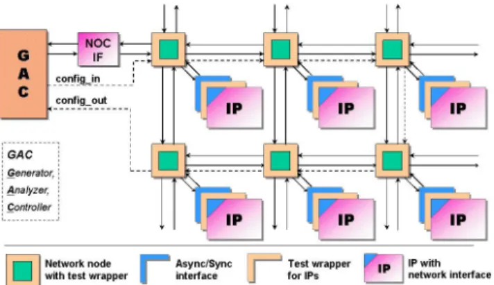
To ease the test of manufacturing defects of the ANOC, we have proposed a DfT architecture as illustrated in Fig-ure 1. This architectFig-ure has been designed for the ANOC but it can be also used for other asynchronous NoCs with any work topology. In this architecture, each asynchronous net-work node is surrounded by a test wrapper in order to improve the controllability and the observability of the nodes. The test
Figure 1. The proposed DfT architecture.
wrapper are used to insert test vectors to the node-under-test or to get out the test results from the node-under-test. In addition, the test wrappers are used with the communication channels between network nodes (i.e. the inter-node links) to estab-lish high throughput TAMs, which do transport the test data. To test a communication channel between two nodes, two test wrappers are used to insert test vectors and to get out the test results.
The proposed test wrappers have been designed and im-plemented in QDI asynchronous logic style for many reasons: well adapted to asynchronous NoC architectures, no dedicated test clock required, and no asynchronous/synchronous inter-face overhead. The reuse of the communication channels al-lows not only to get a high throughput TAM, but also to avoid the wire congestion problem at layout process.
All operations of the test wrapper are controlled by its own control module, named Test Control Module (TCM). The test flows for the whole architecture are established by a dedi-cated 2-bit test configuration channel built by connecting seri-ally all TCM blocks of the test wrappers. An external block, the Generator-Analyzer-Controller (GAC) unit, has also been developed to generate test vectors, to control test flows, and to analyze the test results. This unit is connected to the tar-geted asynchronous NoC via a NoC interface (NOC-IF). The interface between GAC unit and network architecture includes input/output 34-bit communication channels and input/output 2-bit test configuration channels (‘config in’ & ‘config out’). All of this architecture was functionally modeled and validated in SystemC/C++ as described in [11].
3. Asynchronous QDI implementations
To implement the proposed architecture, the Quasi De-lay Insensitive (QDI) asynchronous logic style [10] is used. We use a 4-phase RTZ (Return-to-Zero) signaling protocol for asynchronous channels, associated to a WCHB (Weak-Condition Half Buffer) reshuffling for pipelined stages. To get low power consumption, the full data path (32 bits + BoP + EoP) is entirely designed with the 1-of-4 data encoding
scheme [2], requiring 17 MR[4] QDI connections (an MR[4] connection which encodes two bits is composed of 4 rails and an acknowledge, see Figure 2). The 2-bit test configuration path is also designed with this data encoding scheme, requir-ing an MR[4] connection. The other control signals are de-signed with Dual-Rail (DR) or Single-Rail (SR) codes (a DR connection includes two rails and an acknowledge, and a SR connection includes a rail and an acknowledge).
Figure 2. The 4-phase RTZ MR[4] protocol.
In our architecture, pipeline latch is a basic component. To give an understandable example of asynchronous circuits’ op-erations, an asynchronous buffer made by the juxtaposition of two WCHB asynchronous processes (half-buffers), referred to as asynchronous latches, is given in Figure 3. This 2-bit
Figure 3. A 2-bit QDI asynchronous buffer.
buffer is implemented in QDI asynchronous logic style using the 4-phase RTZ signaling protocol and the 1-of-4 data encod-ing scheme. Therefore, it has 4 rails (in[0], in[1], in[2], and in[3]) and an acknowledge (‘in ack’) at the input port, and 4 rails (out[0], out[1], out[2], and out[3]) and an acknowledge (‘out ack’) at the output port. With this example, we aim at showing the principles that allow storing a data on an asyn-chronous channel.
By considering the timing diagram shown in Figure 2, it is able to understand how this buffer works. Firstly, we suppose that the communication channel between two latches is free, the signal ‘in ack’ therefore gets ‘high’, and there is an arriv-ing data at the first latch’s input. Secondly, we suppose that the
second latch’s output is connected to a receiver. Consequently, the arriving data can be passed via the first latch if the second latch’s output is free (the signal ‘s ack’ is ‘high’). This data is stored on the communication channel between two latch if the ‘out ack’ signal is ‘low’ (because the receiver is not ready to receive a new data). Until the receiver becomes ready to get a new data, it will set ‘out ack’ signal to ‘high’ and the stored data will be passed via the second latch and will be read by the receiver. From this example, we see that the data can be stored on a communication channel in asynchronous circuits by Muller-C-elements. This makes it possible to store test data in the test wrapper.
4. Asynchronous Test Wrapper Realization
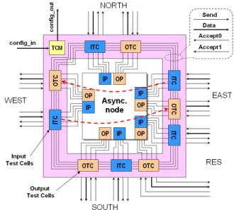
The role of the test wrapper is to transport test vectors to the node-under-test and to get out the test results. In correspond-ing to the number of input/output ports of the ANOC node, our test wrapper is composed of 5 input test cells (ITCs), 5 output test cells (OTCs), and a test control module (TCM), as illustrated in Figure 4. The test cells are interconnected
seri-Figure 4. A network node with the test wrapper.
ally to establish a boundary scan path around the node. The role of the TCM block is to control the test cells to do the test wrapper’s function.
In addition, to reduce test time and to minimize test com-plexity, the possibility of bypass function is alway preferred in DfT architectures. In our case the bypass function allows to reduce the length of test paths by giving short-circuits be-tween the input and the output of test wrappers. With bypass function, only the node-under-test or the channel-under-test is situated in test mode and is connected to the GAC unit, the other nodes may be inactive. In Figure 4, a bi-direction bypass WEST⇔EAST is implemented (indicated by dashed arrows).
4.1. Test cells
The main component of the test wrapper presented in Fig-ure 4 is the “test cell”. The functional operations of the test cells can be described as follows:
In normal mode, communication data are transported from network to node via input test cells (ITCs) and from node to network via output test cells (OTCs).
In test mode, the operations of an ITC can be explained as follows: test data from either the network or the previous test cell are stored on this test cell, and then the stored test data will be transported to either the node-under-test or the next test cell. It is similar for an OTC: test data from either the node-under-test or the previous test cell are stored on this test cell, and then the stored test data will be transported to either the network or the next test cell. All of these operations are controlled by the signals provided by the TCM block.
To implement the above functions, we have developed an architecture of 34-bit test cells as illustrated in Figure 5. It
Figure 5. Architecture of test cells.
is composed of two asynchronous multiplexers (MODE & MUX), two asynchronous splitting blocks (S1 & S2), and an asynchronous merging block (M1). With this architec-ture, communication data are transported from ‘NOC IN’ to ‘NOC OUT’ via MODE in normal mode (i.e., ‘ctrl mode’ = ‘0’). In test mode, test data from either ‘NOC IN’ (if ‘ctrl mux’ = ‘0’) or ‘CELL IN’ (if ‘ctrl mux’ = ‘1’) are stored on the asynchronous channel “LOCAL” between MUX and S2 (as explained in Section 3), then the stored test data will be transported to either ‘NOC OUT’ (if ‘ctrl mode’ = ‘1’) or ‘CELL OUT’ (if no value on the ‘ctrl mode’ signal). It should be noted that without bypass function the ITCs and the OTCs have the same architectures, as described in Figure 5.
4.2. Test control module (TCM)
The operation of the test wrapper is decided by the test configuration frames generated by the GAC unit. In order to reduce the number of control signals provided by the GAC unit, the whole configuration of the TCM is split into 2-bit pieces, which are sent serially to the TCM. In our architecture, each test configuration frame includes of 25 configuration po-sitions (i.e. pieces) of 2 bits (encoded by MR[4] data encoding
scheme), as described in Figure 6. The role of TCM block is to gather the successive configuration values sent on the con-figuration channel until it forms the test concon-figuration frame for the test wrapper. When it has received a complete config-uration frame (by detecting an End-of-Frame (EoF) indication as the last piece of configuration), it has to determine whether the received configuration frame is reserved for the test wrap-per or not. This is done by means of the “Identifier (ID)” field addressing the successive node test wrappers on the configu-ration chain. If the frame identifier corresponds to the one of the test wrapper, the TCM block will generate control signals (according to the configuration frame’s values) to control the test cells.
To implement the above function, the TCM block is com-posed of a “Frame Shifter” block, and a “Transferring” block, as described in Figure 6. The purpose of “Frame Shifter”
Figure 6. TCM architecture and test configura-tion frame.
block is to read a new configuration piece via the input (‘CONF IN’), to shift the configuration frame one position to the right, and to write out the lowest significant configuration piece to the output (‘CONF OUT’). The “Transferring” block is used as a driver to control all test cells. It receives control values from “Frame Shifter” block when an EoF flag is de-tected with a good ID. The outputs of this block are 20 control channels (‘ctrl mode[i]’ and ‘ctrl mux[i]’, i gets values from 0 to 4 for indicating NORTH, EAST, SOUTH, WEST, RES directions respectively).
The explication of all configuration positions of the con-figuration frame is presented in Table 1. Each configura-tion posiconfigura-tion is encoded by an MR[4] (2 bits), the value of each position therefore may be “0”[4], “1”[4], “2”[4], and “3”[4]. The value of “3”[4] is reserved for EoF indication, hence other configuration positions can use up to 3 values. With 3 configuration positions for test wrapper identification, this configuration frame can be used for a NoC architecture with number of nodes up to 27. For larger NoC architectures, we need to add more identification positions. The value of
Table 1. Test configuration frame explanation.
EoF End of Frame indication
ID[2:0] Identification number of the test wrapper EMo[i] Enable ctrl mode signal for output test cell i MCo[i] Value of ctrl mux signal for output test cell i EMi[i] Enable ctrl mode signal for input test cell i MCi[i] Value of ctrl mux signal for input test cell i
M Mode of the test wrapper
Mode (M) may be “0”[4] (normal mode), “1”[4] (test mode), or “2”[4] (bypass mode). The value written on the control channel (‘ctrl mode[i]’) of ITCs or OTCs is the value of Mode position. However, in test mode the ‘ctrl mode’ channel of the ITC i is written only when EMi[i] equals “1”[4], and the the ‘ctrl mode’ channel of the OTC i is written only when EMo[i] equals “1”[4]. The value written on each ‘ctrl mux[i]’ channel of ITCs or OTCs depends on the value of MCi[i] or MCo[i], respectively: the ‘ctrl mux[i]’ channel of the ITC i gets ‘0’ when MCi[i] equals “1”[4], it gets ‘1’ when MCi[i] equals “2”[4]; similarly, the ‘ctrl mux[i]’ channel of the OTC i gets ‘0’ when MCo[i] equals “1”[4], it gets ‘1’ when MCo[i] equals “2”[4]. Examples of test configuration frames will be presented in Section 6.
5. Validation
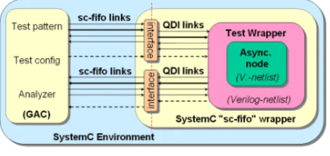
The proposed test wrapper has been implemented and syn-thesized using Cadence Schematic and Design Compiler with STMicroelectronics CMOS 65nm library and TIMA 65nm Asynchronous library (TAL065). To validate this imple-mentation, we have developed a SystemC/Verilog netlist co-simulation platform, see Figure 7. In this platform, the Verilog
Figure 7. Validation platform.
netlist of an asynchronous network node with test wrapper is wrapped by a SystemC wrapper in order to be able to com-municate with other SystemC blocks such as the GAC unit. The SystemC wrapper is composed of SystemC sc-fifo⇔QDI interfaces: sc-fifo⇔QDI MR[4] interfaces used for data and configuration paths; sc-fifo⇔QDI DR for send channels; and sc-fifo⇔QDI SR for accept channels. The goal of this co-simulation validation platform is to have a high speed, unified
platform for multi-level design and validation.
6. Experimental Results
6.1. Test Configurations
According to the test strategies, test configuration sets will be generated by referring to the test configuration frame’s structure, mentioned in Section 4.2. For example, Table 2 presents a test configuration frame for testing the node-under-test on the routing direction NORTH→WEST. This
configu-Table 2. Example of a test configuration frame.
EoF ID Ro-Ri Wo-Wi So-Si Eo-Ei No-Ni M 3 000 02-02 11-01 02-02 02-02 02-12 1 ration frame can be explained as follows: the most significant value (EoF = “3”) indicates the end of configuration frame; the next three values (ID = “000”) means that this configura-tion frame is used for the test wrapper number 0; the lowest significant value (Mode = “1”) puts the test wrapper in test mode; Wi = “01” (i.e. EMi[3] = “0” and MCi[3] = “1”) means that the ITC 3 (WEST) receives test data from the TAM and shifts them to the OTC 2 (SOUTH); So = “02” means that the OTC 2 (SOUTH) in shifting mode, hence the test data is shifted to the ITC 2 (SOUTH); similarly, all of Si, Ro, Ri, No equals “02” means that all of the ITC 2 (SOUTH), the OTC 4 & the ITC 4 (RES), the OTC 1 & the ITC 1 (EAST), and the OTC 0 (NORTH) are in shifting mode, hence the test data is shifted to the ITC 0 (NORTH). Finally, with Ni = “12” the ITC 0 (NORTH) receives the test data from the boundary scan chain and sends them to the node-under-test. After node’s op-erations, with Wo = “11” the OTC 3 (WEST) will receive the test results from the node-under-test and transports them to the analyzer (integrated on GAC unit) via the TAM.
6.2. Test patterns
By studying the functionalities of the network node and considering the data encoding schemes used in our design, the patterns are generated using pseudo-exhaustive testing methodology. Instead of a 35-bit exhaustive testing (32 bits for data path + BoP + EoP + one bit for signaling virtual channel), the test vector is split into many parts. Then we do exhaustive testing for each part. As the data packets of the ANOC [3], a test packet is composed of successive flits. A packet begins by a header flit, followed by one or more data flits. For the header, the “path-to-target” field has to be determined by our test plan (by targeted routing directions). The test data flits can get the 1-of-4 encoded data (“0”, “1”, “2”, and “3” MR[4]) for each two bits.
An example of a test packet (composed of 5 test flits) ac-cording to the above test configuration is described in Table 3. The above test configuration and test pattern allows to test the virtual channel 1 of the node-under-test (Send=“1”) on the
Table 3. Examples of Test Patterns.
BoP-EoP Data Send
TF1 “2”[4] “0000000000000003”[4] “1”[2] TF2 “0”[4] “0000000000000000”[4] “1”[2] TF3 “0”[4] “1111111111111111”[4] “1”[2] TF4 “0”[4] “2222222222222222”[4] “1”[2] TF5 “0”[4] “3333333333333333”[4] “1”[2] TF6 “1”[4] “0000000000000000”[4] “1”[2]
routing direction NORTH→WEST for corrupted data faults, dropped data faults, QDI MR[4] coding violations. The test flit TF1 is a header flit with BoP-EoP=“2”[4], and the last value equals “3”[4] to get the targeted routing direction. The other test flits (TF2, TF3, TF4, and TF5) are test data flits with BoP-EoP=“0”[4]. The last test flit (TF6) is a test flit with BoP-EoP=“1”[4]to indicate the end of the test packet.
6.3. Fault detection
The implemented architecture is able to detect most func-tional faults of the network nodes, for examples, dropped data faults, corrupted data faults, routing direction faults, arbitrat-ing faults (virtual channels, concurrent data conflicts), etc.
To prove the proposed method, we have injected some stuck-at faults at several Muller-C-elements’ input/output pins of the node-under-test to see what the implemented architec-ture is able to give. As results, most of the stuck-at ‘0’ and stuck-at ‘1’ faults are detected. Although we cannot know where exactly the defect is situated, but we are able to deter-mine which input/output controller of network node has a de-fect, and particularly, isolate a path in this controller on which the defect is located. We note that a network node that con-tains defects can still be used in degraded mode (we use only the routing paths that do not contain any defect).
6.4. Latency
The test wrappers are used to improve the testability of NoC architectures, but they give back a supplementary latency for NoC communication in normal mode. This latency equals an asynchronous buffer delay for a pair of an ITC and an OTC (a half buffer delay for each test cell). At a system’s operation frequency of 500M Hz, the added latency is 0.34ns (post-layout measurement). Although the test wrapper gives back an additional latency, there is no change on the communica-tion throughput in normal mode.
6.5. Area
The proposed test wrapper has been implemented using the STMicroelectronics CMOS 65nm technology. The area of a test cell is 8, 560µm2 and the area of the TCM block
is 10, 400µm2. Consequently, a complete test wrapper of 5
ITCs, 5 OTCs, and a TCM block costs 96, 000µm2, i.e. 32.7% of the area of a testable asynchronous network node. However, the area overhead of the whole proposed DfT architecture in our prototype chip (6mm2) is only 576, 000µm2, less than 9% of the total chip area.
7. Conclusions
In this paper, we present the realization and implementation of the asynchronous test wrapper, a basic element of the DfT architecture [11], in STMicroelectronics CMOS 65nm tech-nology (using the TIMA 65nm asynchronous standard cell li-brary). To validate this implementation, a SystemC/Verilog netlist co-simulation platform has also been proposed.
The proposed DfT architecture is targeted to test asyn-chronous NoC architectures (network nodes and communica-tion channels), but it can be also used to test network interfaces and computational resources. Thanks to the reuse of the com-munication channels as a high-speed TAM to transport test data, no dedicated test bus is required. The proposed DfT architecture has been integrated into an actual asynchronous NoC-based SoC prototype chip. The appearance of this sili-con chip is expected on May 2007.
References
[1] J. Bainbridge and S. Furber. CHAIN: a Delay-Insensitive Chip Area Interconnect. IEEE Micro, 22(5):16–23, Sept.-Oct. 2002. [2] J. Bainbridge, W. Toms, D. Edwards, and S. Furber. Delay-Insensitive, Point-to-Point Interconnect using m-of-n Codes. In Proc. of the ASYNC’03, pages 132–140, CA, May 2003. [3] E. Beign´e, F. Clermidy, P. Vivet, A. Clouard, and M. Renaudin.
An Asynchronous NoC Architecture Providing Low Latency Service and its Multi-level Design Framework. In Proc. of the ASYNC’05, pages 54–63, N.Y., March 2005.
[4] L. Benini and G. De Micheli. Networks on Chips: A New SoC Paradigm. IEEE Computer, 35(1):70–78, Jan. 2002.
[5] W. Dally and B. Towles. Route Packets, Not Wires: On-Chip Interconnection Networks. In Proc. of the Design Automation Conf. (DAC’01), pages 684–689, Las Vegas, June 2001. [6] A. Efthymiou, J. Bainbridge, and D. Edwards. Test
Pat-tern Generation and Partial-Scan Methodology for an Asyn-chronous SoC Interconnect. IEEE Transactions on VLSI Sys-tems, 13(12):1384–1392, Dec. 2005.
[7] A. Jantsch and H. Tenhunen (Eds). Networks on Chip. Kluwer Academic Publisher, Feb. 2003.
[8] D. Lattard and et al. A Telecom Basedband Circuit based on an Asynchronous Network-on-Chip. In Proc. of the ISSCC’07, San Francisco, USA, Feb. 2007.
[9] A. Lines. Asynchronous Interconnect for Synchronous SoC Design. IEEE Micro, 24(1):32–41, Jan.-Feb. 2004.
[10] M. Renaudin, P. Vivet, and F. Robin. ASPRO-216: a Standard Cell QDI 16-bit RISC Asynchronous Microprocessor. In Proc. of the ASYNC’98, pages 22–31, USA, April 1998.
[11] X.-T. Tran, J. Durupt, F. Bertrand, V. Beroulle, and C. Robach. A DFT Architecture for Asynchronous Networks-on-Chip. In Proc. of the 11th IEEE European Test Symposium (ETS’06), pages 219–224, UK, May 2006.