HAL Id: hal-01139770
https://hal.archives-ouvertes.fr/hal-01139770
Submitted on 7 Apr 2015
HAL is a multi-disciplinary open access
archive for the deposit and dissemination of
sci-entific research documents, whether they are
pub-lished or not. The documents may come from
teaching and research institutions in France or
abroad, or from public or private research centers.
L’archive ouverte pluridisciplinaire HAL, est
destinée au dépôt et à la diffusion de documents
scientifiques de niveau recherche, publiés ou non,
émanant des établissements d’enseignement et de
recherche français ou étrangers, des laboratoires
publics ou privés.
Efficient energy transfer from Si-nanoclusters to Er ions
in silica induced by substrate heating during deposition
Sébastien Cueff, Christophe Labbé, Julien Cardin, Jean-Louis Doualan,
Larysa Khomenkova, Khalil Hijazi, Olivier Jambois, B. Garrido, Richard Rizk
To cite this version:
Sébastien Cueff, Christophe Labbé, Julien Cardin, Jean-Louis Doualan, Larysa Khomenkova, et al..
Efficient energy transfer from Si-nanoclusters to Er ions in silica induced by substrate heating during
deposition. Journal of Applied Physics, American Institute of Physics, 2010, 108 (6), pp.064302 1-6.
�10.1063/1.3481375�. �hal-01139770�
Efficient energy transfer from Si-nanoclusters to Er ions in silica induced by substrate
heating during deposition
Sébastien Cueff, Christophe Labbé, Julien Cardin, Jean-Louis Doualan, Larysa Khomenkova, Khalil Hijazi, Olivier Jambois, Blas Garrido, and Richard Rizk
Citation: Journal of Applied Physics 108, 064302 (2010); doi: 10.1063/1.3481375 View online: http://dx.doi.org/10.1063/1.3481375
View Table of Contents: http://scitation.aip.org/content/aip/journal/jap/108/6?ver=pdfcov Published by the AIP Publishing
Articles you may be interested in
Resonant structures based on amorphous silicon suboxide doped with Er 3 + with silicon nanoclusters for an efficient emission at 1550 nm
J. Vac. Sci. Technol. B 27, L38 (2009); 10.1116/1.3246406
Photoluminescence from Er-doped Si-rich Si oxides deposited by magnetron sputtering in Ar or Ar + H 2 plasmas J. Vac. Sci. Technol. A 27, 101 (2009); 10.1116/1.3043465
Effect of ion-irradiation induced defects on the nanocluster Si ∕ Er 3 + coupling in Er-doped silicon-rich silicon oxide
Appl. Phys. Lett. 91, 021909 (2007); 10.1063/1.2752538
Sub-nanometric metallic Au clusters as efficient Er 3 + sensitizers in silica Appl. Phys. Lett. 89, 151121 (2006); 10.1063/1.2266229
The 1.54 ‐ μ m photoluminescence from an (Er, Ge) co-doped Si O 2 film deposited on Si by rf magnetron sputtering
Appl. Phys. Lett. 85, 4475 (2004); 10.1063/1.1819514
Efficient energy transfer from Si-nanoclusters to Er ions in silica induced
by substrate heating during deposition
Sébastien Cueff,1Christophe Labbé,1,a兲Julien Cardin,1Jean-Louis Doualan,1
Larysa Khomenkova,1Khalil Hijazi,1Olivier Jambois,2Blas Garrido,2and Richard Rizk1
1
Centre de Recherche sur les Ions, les Matériaux et la Photonique (CIMAP), ENSICAEN, CNRS, CEA/IRAMIS, Université de Caen, 14050 CAEN Cedex, France
2Dept. Electrònica, MIND-IN2UB, Universitat de Barcelona, Martí i Fanquès 1, 08028 Barcelona, CAT,
Spain
共Received 14 May 2010; accepted 22 July 2010; published online 17 September 2010兲
This study investigates the influence of the deposition temperature Tdon the Si-mediated excitation
of Er ions within silicon-rich silicon oxide layers obtained by magnetron cosputtering. For Td
exceeding 200 ° C, an efficient indirect excitation of Er ions is observed for all as-deposited samples. The photoluminescence intensity improves gradually up to a maximum at Td= 600 ° C
before decreasing for higher Tdvalues. The effects of this “growth-induced annealing” are compared
to those resulting from the same thermal budget used for the “classical” approach of postdeposition annealing performed after a room temperature deposition. It is demonstrated that the former approach is highly beneficial, not only in terms of saving time but also in the fourfold enhancement of the Er photoluminescence efficiency. © 2010 American Institute of Physics.
关doi:10.1063/1.3481375兴
I. INTRODUCTION
Silicon-rich silicon oxide matrix doped with Er3+ ions 共SRSO:Er兲 is now a well-known material investigated for Si-based photonics.1 This system can take advantage of the energy transfer from Si-nanoclusters 共Si-nc兲 to erbium ions and then benefits from the high absorption cross section of Si-nc, which is nearly three orders of magnitude higher than the direct excitation cross section of Er ions.2,3Such a mate-rial should, therefore, allow the fabrication of low-cost and silicon-compatible photonic devices 共LEDs, planar optical amplifiers, laser, etc.兲. To achieve an amplifying medium, the coupling between Si-nc and Er ions must ensure the popula-tion inversion, and this requires in turn a careful optimizapopula-tion of the material. The fabrication process appears, therefore, as a crucial step regarding the distance-dependent interactions between the Er3+ ions and the Si-based sensitizers.4–8
It is then essential to nanoengineer the density and distribution of both Er3+ions and Si-based sensitizers within the silica
ma-trix. In this regard, several groups have analyzed the influ-ence of different annealing treatments on the optical perfor-mance of SRSO:Er layers9–13 usually deposited at room temperature共RT兲 before being subsequently annealed at dif-ferent temperatures. Such a process allowed the formation of Si-nc sensitizers and then the observation of Er photolumi-nescence 共PL兲 under nonresonant optical excitation. How-ever, our group has recently observed an Er-PL under these indirect excitation conditions on the as-deposited samples at about 500 ° C.13,14 The Er emission was improved after an-nealing at about 500– 600 ° C, and this aspect was also con-firmed by another team on similarly sputtered layers.15 We have assigned such an observation to the formation of
Si-based sensitizers during the deposition process that are
ex-pected to be very small and dense, ensuring a noticeable coupling with the Er ions. Nevertheless, a careful and sys-tematic examination of the influence of the deposition tem-perature 共Td兲 on SRSO:Er thin films is still lacking. In the
present study, we demonstrate that the deposition tempera-ture governs, on the one hand, the formation of Si-sensitizers in the as-deposited layers, and influences, on the other hand, the composition and density of sensitized Er ions. The rel-evance of such a “growth-induced annealing” is further evi-denced through a comparison with a standard postdeposition annealing bringing into operation the same thermal budget.
II. EXPERIMENTAL DETAILS
Series of SRSO:Er samples were deposited onto a p-type, 250-m-thick silicon wafer, thanks to the magnetron cosputtering of three confocal cathodes共SiO2, Si, and Er2O3兲
under a plasma of pure Argon at a pressure of 2 mTorr. The deposition temperature共Td兲 was varied from RT to 700 °C,
being the maximal temperature that can be applied. The du-ration of all depositions were set to two hours. The power densities applied on the three confocals targets PSiO2
⬇8.88 W/cm2, P
Si⬇1.63 W/cm2, PEr2O3⬇0.44 W/cm2
were kept constant for all depositions.
The Er content was measured by time-of-flight second-ary ion mass spectroscopy共TOF-SIMS兲 measurements. This TOF-SIMS technique was calibrated by a reference SRSO:Er sample in which the Er concentration was accurately mea-sured by Rutherford backscattering. surfaces of deposited layers were analyzed by atomic force microscope 共AFM兲 provided by Digital Instruments 共Nanoscope兲, operating in tapping mode at RT. The Si excess was estimated by a Fou-rier transform infrared 共FTIR兲 spectroscopy approach de-tailed elsewhere.14 The refractive index and the thickness were measured using spectroscopic ellipsometry共SE兲. a兲Electronic mail: [email protected].
JOURNAL OF APPLIED PHYSICS 108, 064302共2010兲
0021-8979/2010/108共6兲/064302/6/$30.00 108, 064302-1 © 2010 American Institute of Physics [This article is copyrighted as indicated in the article. Reuse of AIP content is subject to the terms at: http://scitation.aip.org/termsconditions. Downloaded to ] IP:
Visible and IR PL spectra were obtained using the 476 nm excitation wavelength from an Ar+laser which is a non-resonant wavelength for the erbium ion. The spot size of the laser beam was measured by a “moving knife-edge” method and was found to be around 1 mm at 1/e2 of the maximum
intensity. A 1 m single grating monochromator共Jobin Yvon兲 and a liquid-nitrogen-cooled germanium detector 共North-coast兲 were used to collect the Er-PL while the visible spec-tra were collected with a photomultiplier tube. These mea-surements were made by using the standard lock-in techniques 共SP830 DPS兲 referenced with a chopping fre-quency of 9 Hz. Time-resolved measurements were obtained by the 435 nm excitation wavelength of a pulsed Optical Parametric Oscillator共OPO兲. The pulse duration was ⬃5 ns and the spot size 0.8 mm at 1/e2 of the maximum intensity.
The PL signal of the time-resolved measurements was col-lected by an InGaAs detector.
III. RESULTS AND DISCUSSION A. Structural analyses
The deposition temperature Td is expected to have an
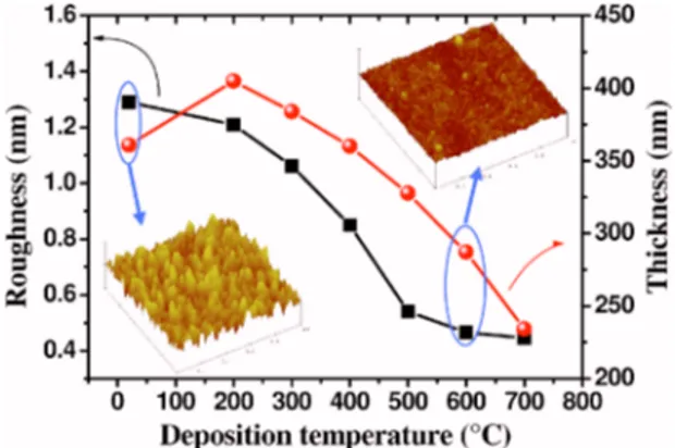
influence on several structural parameters. We have first ana-lyzed the evolution of the surface quality of the deposited layers by AFM techniques. Figure 1 shows the variation in the surface roughness in terms of root mean square共rms兲 as a function of Td, as well as two typical AFM images for two
Td values 共RT and 600 °C兲. The roughness 共rms兲 continu-ously softens from 1.6 to 0.3 nm when Td increases, with a steep decrease for Td between 300 and 600 ° C.
A similar behavior is observed for the thickness共Fig.1兲 which also decreases with Td, from about 380 to 240 nm, i.e.,
a reduction in about 35%. The surface roughness is generally correlated with both mobility and growth rate of the depos-ited atoms, especially in this specific layer-by-layer deposi-tion technique. Indeed, the surface roughness reflects some balance between the deposition rate and the surface mobility of the sticking elements. For example, a high surface rough-ness is expected to result, either from a limited surface bility at a given sputtering rate, or from a high surface mo-bility at a faster sputtering rate. Besides, a high surface mobility should lead to a progressive relaxation of the
net-work through lower distortion of the atomic bond angles and an improved atomic rearrangement, together with better compactness. Thus, the decrease in both thickness and roughness can be explained by the increasing surface mobil-ity of the deposited elements when Td is increased. This lat-ter statement would be further confirmed by a concomitant decrease in the atomic disorder within the film material. We have collected the FTIR spectra on the various films, in order to examine the evolution of the so-called LO4– TO4 doublet
that is known to be indicative of the disorder within the SiO2
matrix.16
Figure2 compares the corresponding FTIR spectra ob-tained at the Brewster incidence angle共65°兲 after being nor-malized on the LO3 peak. One can observe that the intensity
and structure of LO4– TO4doublet are slightly affected when
Td increases from RT to 400 ° C. However, a gradual and
significant decrease in the intensity is observed for Td
⬎400 °C, hence allowing an increasingly better separation between the LO3and TO3peaks. This decrease demonstrates
that a strong reduction in the disorder occurs within the SiO2
matrix when Tdincreases up to 700 ° C. Such a phenomenon
confirms the above-mentioned increasing mobility of the de-posited elements. This leads, therefore, to the following straightforward conclusion: the higher is the deposition tem-perature, the better is the atomic arrangement within the ma-trix.
An optimum reduction in the disorder should result in an improvement of the compactness, together with a more re-laxed network. However, such suggestions explain only partly the decrease in the thickness of the deposited films. Indeed, the expected improvement of the compactness, com-bined to the reduction in the structural disorder, is not suffi-cient to explain the 35% decrease in the thickness. A signifi-cant part of this thickness lowering may be due to a temperature-dependent sticking/desorption rate of the sput-tered elements, already demonstrated for elemental oxygen on Si substrate,17 and/or the creation of volatiles species. Thus, the composition of the thin film may change according to the deposition temperature. The concentrations of the de-posited elements and especially those of the silicon excess and Er ions are important parameters that must be deter-mined.
FIG. 1.共Color online兲 rms roughness measured by AFM and layer thickness measured by SE as a function of deposition temperature Td. Two typical
AFM micrographs共scan area: 1 m2兲 are also shown for the depositions at
RT and at 600 ° C.
FIG. 2. 共Color online兲 Infrared absorption spectra normalized for as-deposited samples, collected at Brewster angle共65°兲. Inset: relative evolu-tion of LO4– TO4peaks intensity according to the deposition temperature Td.
064302-2 Cueff et al. J. Appl. Phys. 108, 064302共2010兲
The silicon excess is defined here as the percentage of elemental silicon present inside the sample in addition to the proportion of Si in stoichiometric SiO2. For the as-deposited
SRSO:Er thin films, the estimate of the Si excess is not straightforward, considering that the transmission electronic microscopy 共TEM兲 observations are unable to detect either the formation of Si-nc or their evolution with Td. This is due to the lack of contrast between the amorphous Si-nc and the silica matrix, as stated by previous studies.9,18Moreover, the smallness of Si-nc in our as-deposited films makes difficult their observation by energy filtered TEM approach.18 Never-theless, a rough estimate of the Si excess content is possible from the analysis of the TO3-peak energy shift evolution in
the FTIR spectra of our SRSO:Er film, as described elsewhere19 and adopted in our previous work.14 However, the above-described atomic disorder induces some shift in the TO3peak that can be misinterpreted as being due to some
Si excess. To overcome this issue, a reference SiO2 sample
doped with Er was deposited for each Tdvalue. Such a
ref-erence sample is considered as free from silicon excess and its TO3 peak is compared to that of the SRSO:Er sample
deposited at the same Td共see Fig.3兲.
It can be seen in Fig. 3 that for both SRSO:Er sample and SiO2: Er reference, the TO3 peak position decreases
when Td changes from RT to 300 ° C共200 °C for the
refer-ence兲, then increases for higher values of Td. The evolution
of the TO3 peak for the SiO2: Er reference is considered as
reflecting an evolution of the atomic arrangement rather than any Si excess. On the basis of these considerations, the Si excess in the SRSO layer has been estimated from the fol-lowing linear relation:
%Siexcess= TO3 ref SiO2− TO3 SRSO:Er TO3 ref SiO2− TO3 Si ⫻ 100, 共1兲 where TO 3
ref SiO2 and
TO3
SRSO:Er are, respectively, the TO 3 peak
wavenumbers of SiO2: Er and SRSO:Er, while TOSi3 is the
TO3 peak wavenumber of Si taken constant for all Td
共960 cm−1兲.
This approach allowed us to subtract the “background disorder” of the sputtered SiO2: Er and hence determine the
corresponding Si excess for SRSO:Er. To note that the FTIR
approach underestimates the amount of Si excess because the Si–Si links within the Si-nc formed during the growth are not detected and then not taken into account. Nevertheless, re-gardless of the absolute value of Si excess, their evolution is considered as reliably described by the FTIR-related esti-mate, as attested by an earlier comparison with our X-ray Photoelectron Spectroscopy共XPS兲 analyses done on similar samples.20
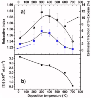
Figure 4共a兲 displays the evolution of the Si excess, as estimated from Eq.共1兲, in function of Td. A first increase in
Si excess is observed when Tdis raised from RT to 300 ° C,
which indicates that the deposition of Si is favored by the rise of Tdup to 300 ° C. This increase is followed by a
“sym-metric” decrease for higher Td values. This behavior of Si
excess is consistent with a similar evolution of the refractive index, n, as determined by SE measurements. To note that n of the SiO2: Er references remains almost constant for all Td
at about 1.46 共not shown兲, i.e., very close to that of stoichi-ometric SiO2共1.45兲. This corroborates the assignment of the
evolution of n for SRSO:Er samples to that of the Si excess. In particular, the decrease in n for Td⬎300 °C, concomitant
to a decrease in Si excess as estimated by FTIR, reflects an
effective lowering of the Si excess. Thus, the estimated
de-crease in Si excess is not only due to an increasing underes-timate originated from further and further formation of Si-nc. In this regards, the Si excess lowering can be provoked by some increasing interactions/reactions between the deposited species, inducing the formation of volatile elements such as SiO for Tdⱖ300 °C, as supported by earlier studies.21–23
Such processes are temperature-dependent, and Tdcan have
also some influence on the concentration NErof incorporated
Er. Indeed, NEr was found to decrease gradually from 3.7
⫻1020 atom cm−3 to 6.1⫻1019 atom cm−3 when T d
in-creases from RT to 700 ° C关see Fig.4共b兲兴. The origin of this FIG. 3.共Color online兲 Evolution of the wave number of SiO2: Er references
and SRSO:Er samples for each deposition temperature.
FIG. 4. 共Color online兲 共a兲 Ellipsometry measurements of the refractive in-dex at 633 nm and Si excess as estimated by FTIR techniques and the formula共1兲in function of Td共the curves are just a guide for the eyes兲. 共b兲
SIMS measurements of the erbium concentration according to the deposition temperature.
064302-3 Cueff et al. J. Appl. Phys. 108, 064302共2010兲
gradual decrease is difficult to identify but might be corre-lated with the increasing reactive character of the sticking mechanism of the sputtered elements when Tdis increased.
B. PL properties
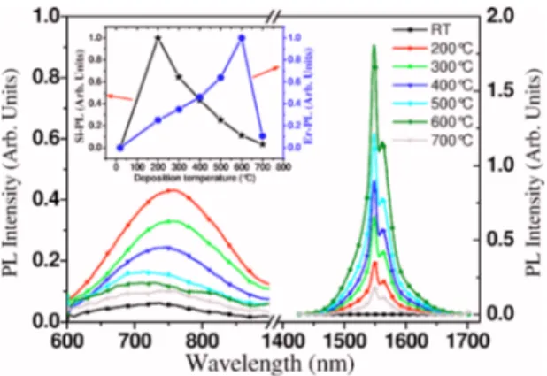
Figure5shows the evolution of the PL spectra recorded on all samples along two main wavelength ranges: the Si-PL feature from 600 to 900 nm range and the Er-PL contribution around 1540 nm. This latter corresponds to the 4I13/2
→4I
15/2 Er3+ transition. The visible emission that peaks at
750 nm for Td= 200 ° C gradually shifts toward 720 nm
when Td is increased to 600– 700 ° C. This visible emission
is assigned to quantum confinement within Si-nc 共Ref. 24兲 that do not transfer their energy to Er3+ ions.3,25 The slight shift to higher energies, in spite of Tdincrease, reflects some
lowering in the average size of Si-nc which is quite compat-ible with the above-commented decrease in Si excess. It is also worth noting that this visible emission was similarly observed and attributed to Si-nc by Savchyn et al.9,26,27 for their samples annealed at 1000 ° C during only 100 s. On the contrary, no contribution is detected in our samples of the so-called luminescent centers 共LCs兲 emitting at around 500 nm.9
The presence of a significant Er-PL in our as-deposited samples共for Tdⱖ200 °C兲 excited with a nonresonant wave-length reveals the occurrence of an efficient energy transfer from Si-nc to Er3+. When T
dis raised from 200 to 600 ° C,
the Er-PL shows a systematic increase at the expense of the Si-nc-PL, hence indicating an increase in sensitized Er ions 共see inset of Fig. 2兲 through Si-nc sensitizers. The sample deposited at RT is suspected to be free from Si-sensitizers, since no Er-PL is detected. Such sensitizers start apparently to form when Td reaches and exceeds 200 ° C. It is worth
noting that the Er-PL intensity increases by a factor of almost 5, in spite of the NEr lowering, when Td is increased from
200 to 600 ° C, before showing an abrupt decrease for Td
= 700 ° C 关Fig. 4共b兲兴. The increase in Td improves also the
quality of the matrix, as demonstrated by the systematic in-crease in the Er emission lifetime, for the longer time decay, from⬃1 ms at 200 °C to 2.5 ms at 700 °C, 共Fig.6兲 which
is almost one order of magnitude higher than the lifetime reported for similar layers containing LCs.9,26
The increase in the Er-PL intensity with Td may
origi-nate from the formation of small Si-sensitizers, as already mentioned, and also from the improvement of the environ-ment of Er3+ ions which is expected to increase the number of optically active Er3+ ions. Indeed, under the resonant wavelength of 980 nm corresponding to a resonant direct excitation of Er 共i.e., without the Si-nc relays兲 from the ground state 4I15/2 to the second excited level 4I11/2, the Er-PL increases systematically up to Td= 600 ° C共see Fig.7兲, reflecting a concomitant enhancement of the number of the optically active ions. On the other hand, the sudden abrupt decrease in the Er PL at 700 ° C for both nonresonant 476 nm and resonant 980 nm excitation lines, suggests some ag-glomeration of the Er ions at this deposition temperature 共700 °C兲, which reduces the number of optically active Er ions,29and consequently the PL intensity.
The deposition temperature thus governs three different phenomena occurring during the growth process:共i兲 the for-mation and growth of Si-based sensitizers, 共ii兲 the variation in both Si excess and Er content, and共iii兲 the improvement FIG. 5. 共Color online兲 PL spectra 共normalized to the thickness兲 at a flux of
5⫻1018 photons cm2/s of both Si-nc 共range 600–900 nm兲 and of Er3+ions
共range 1400–1700 nm兲 for all deposition temperatures. Inset: Si-nc PL in-tensities compared to the Er-PL inin-tensities according to the deposition tem-perature共both normalized to unity兲.
FIG. 6. Behavior of the lifetime values of Er3+at 1.53 m according to the
deposited temperature detectable at the lower excitation photon flux. Inset: a typical PL decay trace of SRSO:Er collected for sample deposited at 600 ° C. Note the PL decay dynamics is biexponential as described in Ref.
28.
FIG. 7. 共Color online兲 Comparison of PL intensity of as-deposited samples recorded at 1.53 m and obtained after indirect excitation共476 nm兲 and direct excitation共980 nm兲. Note that the results corresponding to the 980 nm excitation are multiplied by 104.
064302-4 Cueff et al. J. Appl. Phys. 108, 064302共2010兲
of the quality of the matrix as demonstrated by the decrease in atomic disorder and the increase in the Er emission life-time. Those concomitant effects lead to a positive paradox when the deposition temperature is raised from 200 to 600 ° C: the PL of Er3+ still increases whereas both the Si
excess and the Er concentration get lower. Indeed, the im-provement of the Er-PL up to a maximum for Td= 600 ° C
corresponds to a moderate value of Si excess and almost the lowest NEr. Such an improvement of the PL intensity is,
therefore, arising from the influence of the deposition tem-perature on the growth mechanisms. This leads to some op-timum density and distribution of both sensitizers and Er ions, resulting in better luminescence of Er3+ for the used growth parameters. Two relevant parameters also compete for this enhancement: the number of optically active Er3+ ions which evolves similarly against Td 共Fig.7兲 and the
re-duction in nonradiative recombination, as attested by the raise of the lifetime by a factor of ⬃3 共Fig.6兲.
To give further insight on the influence of the growth-induced annealing, we compare the optical emission of each as-deposited sample grown at a given Td to that recorded from its counterpart film deposited at RT and then annealed for 2 h共i.e., equivalent to the deposition duration兲 at T=Td. This approach allows one to compare the samples having been submitted to the same “thermal budget,” either during deposition or after deposition. The main difference between the intrinsically heated samples during the deposition process and those annealed after RT deposition, lies in the composi-tion evolucomposi-tion: for the former, both NErvalue and Si excess
are varying with Td, whereas these concentrations remain
constant for the latter. To take into account this aspect and accurately compare the two kinds of samples, we define the Er-PL efficiency as the ratio IPLEr/NEr, depending on Td.
Fig-ure 8 compares the Er-PL efficiency according to the tem-perature of thermal treatment, for both as-deposited and post-deposition annealed samples. For the as-deposited films, the Er-PL efficiency increases by a factor of 6–7 when Tdraises
from 200 to 600 ° C. When compared to their counterparts
annealed after RT deposition, their Er-PL efficiency is sys-tematically higher by a factor that reaches a maximum of about 4 for Td= 600 ° C共see inset兲.
This result demonstrates the relevance of layer deposited at a temperature as high as 600 ° C which favors the surface mobility of the sticking elements that can diffuse with rela-tively low activation energy. By comparison, the volume dif-fusion of the elements occurring during the postdeposition annealing requires higher activation energy and result appar-ently in the formation of much less Si-based sensitizers and optically active Er3+ ions. One can therefore infer that the growth-induced annealing is not only a “time-saving” ap-proach but it is also a way to enhance the optical perfor-mance of SRSO:Er thin films. On the other hand, the matrix of the as-deposited samples could be further improved by an additional postdeposition annealing treatment which can be the object of a specific work beyond the scope of this study.
IV. CONCLUSION
In conclusion, the influence of the deposition tempera-ture on the optical properties of SRSO:Er thin films was carefully investigated. The concentration of Er3+ions and the
amount of Si excess were found to change with the deposi-tion temperature. It was also demonstrated that an efficient energy transfer from Si-nc to Er3+ can be obtained for
as-deposited samples at a deposition temperature exceeding 200 ° C, without any annealing. When the deposition tem-perature is further raised to 600 ° C, the Er-PL efficiency is enhanced by a factor of 6–7, compared to 200 ° C, originat-ing from optimum density and distribution of both Si-sensitizers and optically active Er ions, as well as from the matrix improvement. The emission lifetime shows a consis-tent improvement with Td, up to about 2.5 ms. For
compa-rable thermal budget, the growth-induced annealing at Td
= 600 ° C was found to favor the Er-PL efficiency by a factor of about 4, in comparison with the classical annealing per-formed on layer deposited at RT.
1L. Pavesi and D. J. Lockwood, Top. Appl. Phys. 94, 1共2004兲.
2A. J. Kenyon, P. F. Trwoga, M. Federighi, and C. W. Pitt,J. Phys.: Con-dens. Matter6, L319共1994兲.
3M. Fujii, M. Yoshida, Y. Kanzawa, S. Hayashi, and K. Yamamoto,Appl. Phys. Lett.71, 1198共1997兲.
4J. H. Jhe, J. H. Shin, K. J. Kim, and D. W. Moon,Appl. Phys. Lett.82,
4489共2003兲.
5B. Garrido, C. Garcia, P. Pellegrino, D. Navarro-Urrios, N. Daldosso, L.
Pavesi, F. Gourbilleau, and R. Rizk,Appl. Phys. Lett.89, 163103共2006兲. 6F. Gourbilleau, C. Dufour, R. Madelon, and R. Rizk,J. Lumin.126, 581
共2007兲.
7K. Choy, F. Lenz, X. X. Liang, F. Marsiglio, and A. Meldrum,Appl. Phys. Lett.93, 261109共2008兲.
8F. Gourbilleau, M. Levalois, C. Dufour, J. Vicens, and R. Rizk,J. Appl. Phys.95, 3717共2004兲.
9O. Savchyn, F. R. Ruhge, P. G. Kik, R. M. Todi, K. R. Coffey, H. Nukala,
and H. Heinrich,Phys. Rev. B76, 195419共2007兲.
10G. Wora Adeola, H. Rinnert, P. Miska, and M. Vergnat,J. Appl. Phys.102,
053515共2007兲.
11A. Kanjilal, L. Rebohle, M. Voelskow, W. Skorupa, and M. Helm,J. Appl. Phys.104, 103522共2008兲.
12A. R. Wilkinson and R. G. Elliman,J. Appl. Phys.96, 4018共2004兲. 13S. Cueff, C. Labbé, J. Cardin, and R. Rizk,IOP Conf. Ser.: Mater. Sci.
Eng.6, 012021共2009兲.
14K. Hijazi, R. Rizk, J. Cardin, L. Khomenkova, and F. Gourbilleau,J. Appl. Phys.106, 024311共2009兲.
FIG. 8.共Color online兲 Comparison of the evolution of the Er-PL efficiency of the as-deposited samples to that obtained from their counterparts depos-ited at RT and annealed for 2 h at T = Td. The inset compares two normalized
Er-PL efficiency spectra of two SRSO: Er thin films:共i兲 deposited at 600 °C for 2 h共full squares兲 and 共ii兲 deposited at RT and annealed at 600 °C for 2 h共full circles兲.
064302-5 Cueff et al. J. Appl. Phys. 108, 064302共2010兲
15O. Savchyn, R. M. Todi, K. R. Coffey, L. K. Ono, B. R. Cuenya, and P. G.
Kik,Appl. Phys. Lett.95, 231109共2009兲. 16T. Kirk,Phys. Rev. B38, 1255共1988兲.
17M. P. D’evelyn, M. M. Nelson, and T. Engel,Surf. Sci.186, 75共1987兲. 18G. Franzò, S. Boninelli, D. Pacifici, F. Priolo, F. Iacona, and C. Bongiorno,
Appl. Phys. Lett.82, 3871共2003兲.
19P. G. Pai, S. S. Chao, Y. Takagi, and G. Lukovsky, J. Vac. Sci. Technol. A4, 689共1986兲.
20S. Charvet, R. Madelon, F. Gourbilleau, and R. Rizk,J. Appl. Phys.85,
4032共1999兲.
21P. Wickboldt, H. M. Cheong, D. Pang, J. H. Chen, and W. Paul, Mater.
Res. Soc. Symp. Proc. 358共1995兲.
22Y. Takakuwa, M. Nihei, and N. Miyamoto,Jpn. J. Appl. Phys., Part 232,
L480共1993兲.
23D. Gautam, E. Koyanagi, and T. Uchino, J. Appl. Phys. 105, 073517
共2009兲.
24R. Lockwood, A. Hryciw, and A. Meldrum,Appl. Phys. Lett.89, 263112
共2006兲.
25F. Priolo, G. Franzò, D. Pacifici, V. Vinciguerra, F. Iacona, and A. Irrera,J. Appl. Phys.89, 264共2001兲.
26O. Savchyn, R. M. Todi, K. R. Coffey, L. K. Ono, B. R. Cuenya, and P. G.
Kik,Appl. Phys. Lett.94, 241115共2009兲.
27O. Savchyn, P. G. Kik, R. M. Todi, and K. R. Coffey,Phys. Rev. B77,
205438共2008兲.
28A. Al Choueiry, A. M. Jurdyc, B. Jacquier, F. Gourbilleau, and R. Rizk,J. Appl. Phys.106, 053107共2009兲.
29A. Polman, D. C. Jacobson, D. J. Eaglesham, F. C. Kistler, and J. M.
Poate,J. Appl. Phys.70, 3778共1991兲.
064302-6 Cueff et al. J. Appl. Phys. 108, 064302共2010兲