Analysis and Design of Resonant Inductively Coupled Circuits: Application to
Benefit Denial Solutions for the Retail Industry
by Amaury Rony B.S. Mechanical Engineering Ecole des Ponts Paristech, 2011
Submitted to the Department of Mechanical Engineering in partial fulfillment of the requirements for the degree of MASTER OF ENGINEERING IN MANUFACTURING
AT THE
MASSACHUSETTS INSTITUTE OF TECHNOLOGY September 2013
C2013 Amaury Rony. All rights reserved.
MASSACHUSETS N E
OF TECHNOLOGY
NOV 12 2013
U
JBRA RIES
The author hereby grants to MIT permission to reproduce and to distribute publicly paper and electronic copies of this thesis document in whole or in part in any medium now known or hereafter created.
Signature of Author: ...
Amaury Rony Department of Mechanical Engineering August 15, 2013 Certified By: ... .
Prof. David E. Hardt
Ralph E. and Eloise F. Cross Professor of Mechanical Engineering
Thesis Supervisor Accepted By:...
Chairman, Committee for Graduate Students Department of Mechanical Engineering
Analysis and Design of Resonant Inductively Coupled Circuits: Application to
Benefit Denial Solutions for the Retail Industry
by Amaury Rony
Submitted to the Department of Mechanical Engineering in partial fulfillment of the requirements for the degree of
Master of Engineering in Manufacturing
Abstract
ProTeqt develops benefit denial solutions that are electromagnetically deactivated. A magnetic field from the deactivation tablet inductively heats an enabler that provides the proper force to disengage the locking mechanism. Its latest design was not functional at one inch above the deactivation tablet, because of significant efficiency losses in the electromagnetic energy transfer. This is problematic when the product's package is thick. In order to improve the maximal functional distance, an LC circuit is inserted inside the locking device. This thesis describes the optimization and integration of the circuit, used as a weakly coupled electromagnetic resonator in wireless energy transfer. The most efficient resonator design is proposed, under the inherent constraints of this application. It is then tested in real situation in order to evaluate the failure rate of the complete device. Some modifications of the enabler are proposed and discussed to maximize the reliability. Finally, a simulation is conducted to test the sensitivity of the results to the circuit manufacturing variability. Under several clearly stated assumptions, it appears that the manufacturing variability of the hand-made enabler is the most significant, although it does not threaten the reliability of the current locking mechanism.
Thesis Supervisor: David E. Hardt
Title: Professor of Mechanical Engineering
Acknowledgements
First of all, I want to thank my excellent teammates: Mitch Krogman and Tianyu Zhu. They brought great ideas all along the project and I heavily benefited from their different backgrounds to learn something new almost every day.
I am very grateful to Dan Bean, senior mechanical engineer at ProTeqt. During the entire project, he was extraordinary available and helpful. Despite the fast-pace at which every start-up runs, he always found time to respond to our numerous inquiries and provide us with valuable information.
Many thanks to Dr. David Hardt, my adviser. He was always there to answer our questions and question our certitudes. I really appreciated that he kept the door of his office open to help us overcome all the obstacles we faced.
I also give thanks to all the ProTeqt's staff and affiliates: John Berg and George Raniuk who proposed and launched this internship, John LaMalva who introduced us to ProTeqt's marketing, Dimitar Bentchev for his help over the lock mechanism and Stephen Kusy who always knew where the missing tool for each of our experiments was.
I thank Jenifer Craig for carefully following up the writing progress of this thesis. Thanks also to Jose Pacheco who managed the logistics of the MEngM internships (and fed us so often).
Last, but far from least, I express my huge gratitude to my parents and all the people who supported me during this year at MIT. I dedicate my thesis and all my work to them.
Table of Contents
A b stra ct ... 3 A ck n o w le d g e m e n ts ... 4 T a b le o f C o n te n ts... 5 List o f F ig u re s ... 9 List o f T a b le s... 1 2 Chapter 1 Introduction ... 131.1. General Research Topic ... 13
1.2. Need for Benefit Denial Solutions against Retail Theft ... 13
1.3. Product Com ponents and Performance ... 14
1.3.1. Deactivation Tablet... 14
1 .3 .2 . M e ch a n i ca l Lo ck ... 15
1.3.3. Im proving Product Performance ... 16
1.4. Resonant Coupling ... 17
1.5. Design and Production of LC Circuits ... 17
1.6. Problem Statem ent ... 18
1 .7 . T a sk D iv isio n ... 18
Chapter 2 Electrom agnetism and Inductive Coupling ... 20
2.1. M agnetic Field Due to Current... 20
2 .1 .1 . Ed d y C u rre n ts ... 2 0 2 .1 .2 . S k in Effe ct... 2 1 2.1.3. Selection of M aterials and Thickness ... 22
2.2.1. Magnetic Field Strength at a Coil Axis ... 23
2.2.2. M agnetic Flux and Inductance ... 25
2 .3 . In d u ctiv e C o u p ling ... 2 6 2 .4 . R e so na nt C o u p ling ... 2 8 2 .5 . A p p lica tio n s ... 2 9 2 .5 .1 . R F ID ... 2 9 2 .5 .2 . W ire le ss P o w e r... 3 0 Chapter 3 LC Circuit M anufacturing ... 32
3.1. Inductor M anufacturing ... 32
3.1.1. Chem ical Etching ... 33
3 .1.2 . C o il W in d ing ... 3 4 3 .1 .3 . Sc re e n P rin ting ... 3 4 3 .2 . C a p acito rs ... 3 5 3 .3 . So ld e ring T ech n iq ues ... 3 6 Chapter 4 Physics of the Problem and Theoretical Analysis ... 37
4.1. Analysis of the Coupling ... 37
4.2. Theoretical Optimization of the Coil ... 39
Chapter 5 Coil and Circuit Design ... 42
5 .1 . O b jectiv e ... 4 2 5 .2 . D e sig n C o n straints... 4 2 5.3. Experimental Apparatus ... 42
5.4. Preliminary Experiments ... 43
5.4.1. Evaluation of the Apparatus... 43
5.4.2. Experimental Output ... 45
5.4.3. Distance Effect on Natural Frequency ... 46
5.5.1. Response surface of the Current... 47
5.5.2. Efficiency of the Coupling ... 48
5 .6 . O ptim izatio n R e sults ... 50
5.6.1. Optimal Secondary Coil... 50
5.6.2. Effect of Enabler on the Resonant Frequency and the Coupling Quality ... 52
5 .7 . O th e r C o il D e sig n s ... 5 5 5.7.1. The Case of Litz W ire Coil... 55
5.7.2. The Case of Thin W ire Coil ... 56
Chapter 6 M echanical Lock Analysis... 57
6 .1 . O bje ctiv e... 5 7 6.2. Introduction to the M echanical Lock ... 57
6 .3 . M e cha n ism A n a lysis ... 58
6.3.1. Analytical Calculations ... 58
6.3.2. Finite Element Analysis (FEA)... 59
6 .3 .3 . E m p irica l T e sts... 5 9 6 .1. Ena b le r Fo rce A n alysis ... 6 1 6 .1 .1 . O bje ctiv e s... 6 1 6.1.2. Experimental Apparatus ... 61
6 .1 .3 . D ata C o lle ctio n ... 6 2 6 .2 . Lo ck Pe rfo rm a nce... 6 6 Chapter 7 Simulation of LC Circuit Variability ... 69
7 .1 . O bje ctiv e s ... 6 9 7.2. Simulation of Experimental Data ... 69
7.3. Frequency Distribution ... 70
7 .4 . Fit o f Efficie n cy P lo t... 7 2 7 .5 . Fo rce D istrib u tion ... 74
7.6. Discussion on the Component Quality ... 76
Chapter 8 Conclusions and Future W ork ... 77
8 .1 . R e co m m e n d atio ns ... 7 7 8 .1 .1 . LC circu it d e sig n ... 7 7 8 .1 .2 . Lo ck M e cha nism ... 7 8 8.1.3. Effect of LC Circuit Variability on Lock Reliability ... 78
8 .2 . F u tu re W o rk ... 7 9 8 .2 .1 . M icro -U S B Lo ck ... 7 9 8 .2 .2 . P roT e q t B u siness ... 7 9 R e fe re n c e s... 8 1 A p p e n d ix ... 8 3 A. Theoretical Calculation of Resistance and Geometric Factor... 84
A .1 . R e sista n ce ... 8 4 A.2. Geometric Factor... 85
A .3 . S p re a d sh e e t ... 8 5 B. Drawing of LC Circuit Site inside the Lock. ... 87
C. Current Estimation in the Secondary Circuit ... 88
D. Frequency Shift due to Distance ... 90
E. List of M anufactured Coils... 93
List of Figures
Figure 1: The thumb drive lock (Left) and the CD-disk lock (right). Locking mechanisms are signified by th e p a d -lo ck sy m bo l... 1 5 Figure 2: External hard drive with packaging requires a stronger field. This packaging, being targeted by
ProTeqt, leaves the lock at 1 inch above the tablet. ... 16
Figure 3: Typical diagram for an LC circuit where L is the inductor and C is the capacitor... 17
Figure 4: Schematics drawing of current and magnetic field in a conductor with alternating current. I (red arrows) is the current passing thought the conductor. It induces the magnetic field H (blue loops), which itself creates the loops of current l ... 21
Figure 5: Current-carrying Loop and associated magnetic field along the central axis... 24
Figure 6: Magnetic Field along the loop axis, versus the loop radius (log-log scale). Loop radius is 1 mm a n d cu rre nt is 1 A in e q . (2 .6 ). ... 24
Figure 7: Electric circuit of the coupling... 27
Figure 8: Voltage gain versus frequency, for a coupling coefficient k = 0.1. This figure was plotted from equations derived in section 4.1, w here u2 = V... 29
Figure 9: Typical Strongly Coupled Magnetic Resonance (SCMR) System. TX is the transmitting helix. RX is th e re ce iv in g h e lix . [1 1 ]... 3 1 Figure 10: Schem atic of a typical etching process... 33
Figure 11: Typical shapes and sizes of capacitors... 35
Figure 12: Diagram of the two coupled circuits. Primary circuit (left) and secondary circuit (right)... 37
Figure 13: Current in the secondary circuit (coded unit) versus the number of turns and the gage size .. 41
Figure 14: Response surface comparison for tests run on a working deactivator (left) and tests run on the expe rim ental ap paratus (right) ... 44
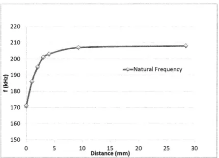
Figure 15: Natural frequency of the system versus the distance between the two antennas ... 47
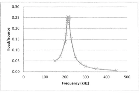
Figure 16: Transfer Function Plot for Coil #1 (9 turns, AWG 24, 1pF capacitance)... 49
Figure 17: Response surface in current for various coil characteristics. ... 50
Figure 18: Induced current in secondary coil versus wire gage and number of turns. Theoretical model (left) and experim ental response surface (right)... 51 Figure 19: Efficiency Plot in current of coil #1(9-turn and AWG 24) with (grey) and without (black) the e n tire lo c k ... 5 3
Figure 20: Efficiency Plot in current for coil #1 (9 turn and AWG 24). Without enabler (dash), with half of
an enabler (grey) and a full enabler (black) ... 54
Figure 21: Efficiency Plot in current. Comparison between litz wire coil and 9-turn AWG 24 coil (#1). Without enabler and with full-size enabler ... 55
Figure 22: Regular coil design (left) and thin wire coil design (right)... 56
Figure 23: Schematic of internal mechanism of the micro-USB lock, developed by ProTeqt... 58
Figure 24: Constraints and load applied in the FEA. Small arrows are for completely fixed surfaces. Long arrows are for force from the enabler... 59
Figure 25: Disengagement force (solid) and mean force (dash) distributions ... 60
Figure 26: Functional diagram of the experimental apparatus... 62
Figure 27: M odel of an enabler constraint fixture... 62
Figure 28: Individual value plot of force vs. activation time using a full enabler on the deactivation tablet ... 6 3 Figure 29: Force distribution for full sized enabler (solid) and half-sized enabler (dash). Right: On tablet. Left: O ne in ch above the tablet... 65
Figure 30: Force distribution. Small dash: disengagement force. Large dash: half sized enabler at 1" above th e ta b le t ... 6 6 Figure 31: Comparison of efficiency plots at three different resonant frequencies: 220 kHz, 210 kHz (-5%) a n d 2 5 0 k H z (+ 1 5 % ) ... 7 0 Figure 32: Histogram of the LC circuit resonant frequency ... 71
Figure 33: Plot of fit for efficiency data with respect to frequency... 73
Figure 34: Efficiency at 220 kHz vs. resonant frequency of the circuit... 73
Figure 35: Histogram of the LC circuit efficiency at 220 kHz... 74
Figure 36: Histogram of the force generated by the half sized enabler ... 75
Figure 37 : Eq u ivalent C o il M odel... 84
Figure 38: Material Properties (input). Here, copper. ... 85
Figure 39: Coil Characteristics (input)... 86
Figure 40: Resistance of the wire ... 86
Figure 41: Geometric Factor of the Coil... 86
Figure 42: Drawing of LC circuit location inside the lock. Unit is inch. ... 87
Figure 43: Electric Model of the Coil... 88
Figure 45: Resonant frequency of the coupling versus the coupling coefficient. Dash line is the natural frequency of the secondary LC circuit. ... 91 Figure 46: List of Manufactured Coils ... 93 Figure 47: Beam bending model used for analytical calculations. ... 94
List of Tables
Table 1: Maximum Voltage for the 6 different coils ... 45
Table 2: Maximum Induced Current through the secondary circuit ... 46
Table 3: List of LC circuits for experimental current response surface... 47
Table 4: Current (coded unit) versus number of turns and gage size... 52
Table 5: Optimal deactivation time for each experiment ... 64
Table 6: Average force for different levels of confinement (full sized enabler, on the tablet)... 64
Table 7: Distribution characteristics ... 65
Table 8: Probability of failure for each of the four deactivation scenarios, with t-distribution ... 67
Table 9: Probability of failure for each of the four deactivation scenarios, with normal distribution... 67
Table 10: Frequency histogram summary... 72
Table 11: Efficiency vs. Frequency Regression Summary... 72
Table 12: Efficiency histogram summary ... 74
Table 13: Force histogram summary ... 75
Table 14: Resonant frequency distributions ... 76
T a b le 15 : Fo rce d istrib utio ns... 7 6 Table 16: Spring force calculation ... 95
Chapter 1
Introduction
1.1.
General Research Topic
The foundation of this thesis is centered on ProTeqt Technologies, a company dedicated to providing anti-theft devices (known as "benefit denial solutions") for the electronics retail industry. In particular, we are developing a technique that can be used to expand their product functionality, based upon a mechanical locking mechanism for a Micro USB hub. More explicitly, we are developing components and understanding parameters that will increase the distance from a disabling device their technology can be used by extending a magnetic field via resonant coupling.
1.2.
Need for Benefit Denial Solutions against Retail Theft
Global retail theft has increased dramatically in recent years, driven by the expansion of online marketplaces [1]. Large online market places such as EBay have given rise to organized retail theft. These online markets make buying and selling stolen items easier than ever. Despite huge investments from retailers and manufacturers (more than $28 billion in 2011 [2]), this plague has continued to grow steadily. The most common solution to prevent theft in retail stores is an electronic article surveillance (EAS) system that alerts the retailer if a product passes through the doors prior to purchase. EAS systems have the limitation that the retailer still has to respond to the alert and this response is often hesitant. In some cases, retailers explicitly tell their employees not to confront those suspected of theft. Increased shrinkage, coupled with non-effective EAS systems, has lead retailers to restrict consumer access for high-theft products (e.g. locking glass or back room cages). However, these actions are known to significantly decrease sales. Moreover, these solutions attempt to address theft only at the point of sale. They fail to address the largest component of shrinkage in the retail industry: organized theft throughout the supply chain (53% of theft in North America [2]).
As a result, retailers are looking for solutions that will provide more security than current theft prevention methods. They are interested in eliminating the motivation to steal: the resale or use of the product. ProTeqt Technologies has addressed this solution by developing a new type of mechanical lock system that temporarily disables the product, rendering it unusable until it is legally
purchased. At the point-of-sale, a deactivating tablet recognizes the product using a RFID tag embedded in the packaging. It then emits a certain electromagnetic signal, based on the product, that deactivates the mechanical lock. If the product is stolen, the lock cannot be removed without damaging the product. Furthermore, their solution can also be easily integrated with current EAS systems using existing RFID tag.
1.3.
Product Components and Performance
ProTeqt's system is comprised of three key elements: the deactivation tablet, cloud database, and mechanical lock. The research covered by this thesis focuses on two of the three elements: the deactivation tablet and the mechanical lock. However, to fully understand ProTeqt's technology and the sequence of events that takes place, we must briefly consider all three elements.
At the point of sale, the sales clerk first scans the product containing the ProTeqt's lock. The RFID is then recognized, allowing the system to look in the ProTeqt database for data corresponding to that particular product. If the product has not previously been unlocked, a certain frequency is taken from the cloud database that coincides with the product at hand. The clerk then positions the product in such a way that the lock is directly over the center of the tablet. With the product in position, the tablet creates a strong electromagnetic field at the appropriate frequency to deactivate the mechanical lock. The customer takes the product home, and uses his or her product as if the
lock was never there. They are able to simply remove the lock and throw it away.
1.3.1. Deactivation Tablet
The deactivation tablet is a highly integrated computer system. The system uses RFID detection to recognize products, an Internet connection to access the cloud database, LED lights to guide the product to the center of the tablet, a function generator to produce certain frequencies, and finally a large coil to generate an electromagnetic field. The tablet must be small and unobtrusive, to provide easy integration at the point of sale.
ProTeqt has contracted the design and manufacturing of the deactivation tablet to MACK Technologies', whose expertise is in circuit board and complex system assembly. While we may not be designing, or analyzing the system for manufacturability, we need to understand the full
functionality and design parameters of the deactivation tablet to further understand the effects it has on other components like the mechanical lock.
1.3.2. Mechanical Lock
The mechanical lock is a small device that is added to a consumer product in a manufacturing stage. The lock is designed to eliminate key features of a product. By encapsulating and interacting with the consumer product, both internally and externally, the device is completely protected from use if not legally purchased. Inside, the lock contains a mechanism that will disengage itself from the internal portion of the consumer product. When disengaged, a spring pops the lock off the product inside the packaging. This action is completed at the point of sale, when the lock receives the proper
magnetic field. The deactivation mechanism is explained with more details in chapter 6.
The lock design is highly dependent on key product features that can be used to render the product unusable. At the time of this project, locks have been designed for two product lines: USB thumb drives and CD-type disks (See Figure 1). For the USB thumb drives, the lock is attached to the male plug. An improper attempt to remove the lock will permanently damage the plug, rendering the USB drive useless. For the disks, the lock secures the disk to its case. Here, improper removal will simply break the disk.
1.3.3. Improving Product Performance
ProTeqt has complete control over their mechanical locking device and deactivation tablet, but they must be compatible with numerous types of locking methods (e.g. USB, disk, etc.) and packaging. In the case of the USB thumb drives and the disks, the packaging is very slim, allowing the lock to be
close to the deactivation tablet. Once the magnetic field is created, the lock is easily deactivated. Because magnetic fields degrade at distance, products that are embedded in thicker packaging (Figure 2) have proven to be more difficult to unlock. ProTeqt has begun to investigate solutions that will provide deactivation of the mechanical locks at a distance of 1 inch from the tablet.
ProTeqt, having developed two unique applications for their technology (USB thumb drive, and CD-type disk), is ready to move forward in the development for a new Micro USB lock. This lock will perform similarly to the USB thumb drive lock, in that it will interface with the consumer product both internally and externally. The Micro USB hub uses a smaller profile than the standard USB hub, introducing some new design challenges. However, the Micro USB lock is used far more prevalently and with more expensive products than the standard USB. Moving forward, ProTeqt would like to achieve the functionality of the Micro USB lock at 1 inch above the tablet surface.
1.4.
Resonant Coupling
As stated above, the objective of ProTeqt is to achieve unlocking at one inch from the tablet. Among several potential solutions, ProTeqt chose to explore and implement the effects of resonant inductive coupling. Resonant inductive coupling is a means to transfer wireless energy through two coils that are tuned to resonate at the same frequency. We can effectively use resonant inductive coupling to extend the magnetic field created by the deactivation tablet. Moving the field closer to the mechanical lock will increase the effectiveness of the field at distance. Furthermore, this solution allows ProTeqt to postpone a redesign of the deactivation tablet. Instead, a simple component can
be designed that will allow the wireless transfer of energy: an LC circuit.
1.5.
Design and Production of LC Circuits
To extend the field, we need to develop an LC circuit. An LC circuit is a circuit comprised of an inductor and a capacitor. This circuit is typically drawn as shown in the figure below (Error! Reference source not found.). By placing the small circuit inside the mechanical lock, we can extend the magnetic field so that it is actually formed inside the lock. Although an LC circuit is simple (an inductor coil connected to a capacitor), it must be designed to work at maximum efficiency. The circuit can be tuned to operate most efficiently at a certain frequency. However, because the LC circuit will be operating inside the mechanical lock, we must consider the interaction and effects of the existing components of the lock.
LIC
Figure 3: Typical diagram for an LC circuit where L is the inductor and C is the capacitor
Moreover, the performance of the circuit is dependent on the quality of manufacturing. Thus, the effects of manufacturing variability must be understood, controlled, and minimized.
Finally, as the circuit is inside the lock, it is disposable and must be manufactured at low cost, and on the order of millions of units per year. The production rate and cost are two important parameters that must be considered and optimized from the very beginning of the design.
1.6.
Problem Statement
The goal of this project is to develop the initial idea of a field repeater using resonant inductive coupling. There were multiple challenges, from theoretical physics to manufacturing issues. This thesis only considers those we faced while working at ProTeqt. It must be noted that some tasks were distributed among ProTeqt's partners and are out of the scope of this thesis.
This project was conducted through three phases. First it was necessary to understand the principle of radio frequency heating, physical mechanisms of a field repeater, and optimizing the design of an LC circuit. We focused especially on the coil and LC circuit. For purposes of testing, it was easier and more flexible to design for a wire coil. Preliminary experiments were conducted to characterize the circuit: (1) the geometry and the shape of the coil, (2) the design parameters (number of turns, wire gage and number of layers), (2) the capacitance, and (3) the resonant coupling efficiency. From this study, a second design was proposed for the manufacturing processes that can only achieve thin conductive lines (i.e. high resistance).
In the second phase, the unlocking mechanism is analyzed to understand the interaction between the mechanical parts and the electronic circuit. The purpose of this stage is to guarantee the reliability of the product after inserting the LC circuit.
Finally, in the last phase of the project, different manufacturing methods were investigated: winding, etching, screen printing and inkjet printing. They were analyzed according to three criteria: (1) feasibility of the design, (2) production rate capability, and (3) production cost. Following this analysis we need to define and understand the manufacturing processes and techniques that would be appropriate to produce the circuit, given our constraints. For each of these steps, we highlight the key decision factors and provide recommendations.
1.7.
Task Division
Based upon the three phases of the approach, tasks were divided among the three group members: Mitchell Krogman, Amaury Rony, and Tianyu Zhu. Even though the thesis project at hand has been completed by the collective group, each team member took the lead on one of the three phases, and
delegating responsibility for tasks essential to completion as needed. Theoretical physics and coil design was under the responsibility of Amaury Rony. Mitchell Krogman led the work on the unlocking mechanism and its interaction with the LC circuit. Finally, Tianyu Zhu took responsibility of the manufacturing process analysis and selection.
Chapter 2
Electromagnetism and Inductive Coupling
2.1.
Magnetic Field Due to Current
This section intends to give the minimal background about Electromagnetic theory that is necessary to understand inductive coupling. For more extensive information, the reader is invited to refer to a detailed handbook like [3]. To illustrate the principles of induction, we first present the principles of induction heating. Even though the project covered by this thesis does not focus on this heating method, this is the fundamental principle for every lock at ProTeqt.
Induction heating is a method to heat an electrically conducting object using electromagnetic induction. An inductive heater consists of an inductor excited with an alternating current. According to Faraday's Law, such changing current creates a changing electromagnetic field around the inductor. When the electrically conducting object is placed inside this field, eddy currents are generated within the conductor. This phenomenon causes Joule heating, owing to losses in the conductor. Compared to traditional heating method, induction heating does not require direct physical contact as the energy is
transferred through electromagnetic waves.
2.1.1. Eddy Currents
French scientist Fran ois Arago first discovered eddy currents in 1824 [4]. When a conductor is placed in a changing magnetic field, circulating eddies of current are created inside the conductor. The name eddy current comes from the analogy of circulating water in fluid dynamics. In a non-zero resistivity conductor, the eddy current induced will generate Joule heating and electromagnetic forces. The current will become greater with either a stronger magnetic field or a higher frequency magnetic field. According Lenz's law, the eddy current will flow in a direction such that the magnetic field created by the current will oppose the magnetic field that induces the current. In another word, the eddy current will create a
2.1.2. Skin Effect
With direct current, current density is uniform through the entire cross section of the conductor. When the current becomes alternating, the magnetic field at the center of the conductor increases as the frequency increases, due to the combined effect of conductivity and permeability. The magnetic field creates a current in the opposite direction of the current flowing through, making it more difficult for the current to flow in the center. This is called reactance. Because of the reactance at the center, the current density is the lowest there and the largest near the surface of the conductor, where the reactance goes to zero. This concentration of current at the surface is named the "Skin Effect".
1W
t ti t
t
Figure 4: Schematics drawing of current and magnetic field in a conductor with alternating current. I (red arrows) is the current passing thought the conductor. It induces the magnetic field H (blue loops), which itself creates the loops of current I, In order to acknowledge the skin effect on the resistance of the conductor, the skin depth needs to be estimated [5]. The AC current density decreases exponentially with the depth from the surface. The skin depth is defined as the distance into a conductor at which is current density falls to -= 37% of its value
e along the surface. The skin depth can be expressed as:
1
6= (2.1)
where
f
is the frequency of the current, P = prIo is the absolute permeability of the medium2and a is the conductivity of the material.
For example, for a copper wire carrying an AC current of 220 kHz, the skin depth is 0.141mm. It means that 63% of the current flowing in a copper wire will flow within a distance of 0.141mm to the surface. The effective resistance can be calculated as current flowing uniformly through a layer of thickness 6 with the DC resistivity of that material. The effective cross-sectional area can be approximately represented by:
Aeff = 2Tr , 6 (2.2)
where r is the radius of the wire.
Then, the AC resistance is:
r
RAc RDC (2.3)
All the equations shown above are based on the assumption that the skin depth is significantly smaller than the radius. If the skin depth has the same order of magnitude as the wire radius, the AC resistance at low frequency (below 1 MHz) can be calculated using the following equation:
Rlowfreq ~ R d + (2.4)
48airwS2 where 1 is the total length of the wire.
The first consequence of the skin effect is the increase of resistance, as the skin depth decreases. The value of skin depth is inversely proportional to the square root of the current frequency and the material permeability (see eq. 2.1). Depending on the application, a small skin depth may be an advantage or disadvantage. For instance, if the skin depth is small there will be a large effective resistance. If the goal is maximizing current flow this is a disadvantage, but if the goal is Joule heating (as is the case here) a small skin depth is an advantage. To maximize Joule heating two design strategies can be considered: the selection of materials and thickness.
2.1.3. Selection of Materials and Thickness
The selection of material is critical for the effectiveness of heating. Only conductive materials can be used for induction heating because eddy current needs to flow in the object to generate heat. Even though eddy currents can occur in any conductor, iron and its alloys respond better than aluminum and copper to induction heating owing to their ferromagnetic nature. With same alternating current,
ferromagnetic materials have significantly smaller skin depth, resulting greater resistance. Therefore, more Joule heat is created.
For materials that are thinner than their skin depth at the desired frequency, the skin effect is no longer important. The resistance of the material is only determined by the thickness and the material resistivity. In this case, aluminum and copper can perform just as well as iron.
2.2.
Magnetic Field in a Coil
2.2.1. Magnetic Field Strength at a Coil Axis
Every current, i.e. a flow of moving charges, is associated with a magnetic field. This magnetic field magnitude is represented by the magnetic field strength B (in Teslas). The magnetic field generated by a line current within a wire is derived from Biot-Savart law [3]. That is
B = Idlx Q (2.5)
Q 47T
QP2
L
Q
is the point of observation.P is the center of the elementary element dl.
I
indicated the intensity and the direction of the current at P. 1gp is an elementary vector fromQ
to P.y is the absolute permeability of the medium
From this equation, it is possible to find the magnetic field along a single circular loop of radius a and that carries a current .We are especially interested in the magnetic field B, along the axis of the loop. It
Bz
Figure 5: Current-carrying Loop and associated magnetic field along the central axis
The magnitude of the field is
Bz +- a 3
2 (Z2 + a2)-f
(2.6)
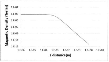
To understand the effect of distance, the magnetic density from eq. (2.6) is plotted as a function of the distance from the loop, with a = 1mm and I = 1A (see Figure 6).
1.E-01 (A 1.E-03 & 1.E-05 C 4) 1.E-07 ' 1.E-09 1.E-11 1.E-13
1.E-06 1.E-05 1.E-04 1.E-03 1.E-02
z distance(m)
LE-01 1.E+00
Figure 6: Magnetic eq. (2.6).
Field along the loop axis, versus the loop radius (log-log scale). Loop radius is 1 mm and current is 1 A in
As long as the distance from the conductor is smaller than the radius, the magnetic field remains approximately constant. However the magnetic density decreases rapidly as the measuring point is
moved further away from the center of the loop. In free space, the decay is 60 dB per decade. It has been shown experimentally that the slope flattens out to 20 dB per decade in the far field [6].
As will be discussed below, a flat spiral coil can be used to increase the magnetic field by increasing the number of loops. A spiral coil can be seen as a certain number of concentric loops with different radii (a,, a2, a3...), and potentially with N layers. In this case, the total intensity of the magnetic field along the
axis of the coil is the superposition of the magnetic field intensities generated by each single loop [6].
Bz I a? 3 (2.7)
N i 2(z2 +a 2 2
The magnetic field is often associated with another field, closely related to B: the magnetic strength H (in Ampere per meter). For the purpose of this thesis, we do not consider the magnetization of the material. In this case, both fields are proportional:
B = Pr PoH (2.8)
For air, pr ~
2.2.2. Magnetic Flux and Inductance
The line along which the magnetic strength is constant is called line of magneticflux. We are interested in the magnetic flux, i.e. the total number of flux lines passing through a given surface. The magnetic flux '4 is proportional to the field density B and the area:
(D = B. A (2.9)
Going back to the current-carrying loop, it is now possible to define and calculate its inductance L.
L = T (2.10)
where cD is the magnetic flux through the inside surface of the loop.
According to eq. (2.6) and (2.9), the magnetic flux is
yla2
a - xa 2
2a3 (2.11)
Thus, the inductance of the loop is
L =
wa
2 (2.12)
It is noticed that inductance does not depend on the current. It only depends on the material properties and the geometry layout. This remains true for more complicated inductors. According to eq. (2.7) and (2.9), the inductance of a spiral coil is the sum of the inductances of each single loop.
2.3.
Inductive Coupling
If a second conductor loop is located close to the first one, a portion of the magnetic flux (P21 from the
first loop is passing through the second one. The two conductors are now coupled. As for inductance (also known as self-inductance), we define the mutual inductance M2 1 of conductor loop 2 in relation
with conductor loop 1 as:
*21
M2 1
-I, (2.13)
In a similar way the mutual inductance of conductor loop 1 in relation with conductor loop 2 is
12 Al12 -=2
It has been shown that both mutual inductances are equal [6] i.e.
M12 = M2 1= M (2.15)
The mutual inductance gives a sense of the quality of coupling between the two inductors. In order to make it independent of their geometric characteristics, the coupling coefficient k is introduced:
M
k = (2.16)
JLL2
where L1 and L2 are respectively the self-inductance of the primary and the secondary inductors.
Continuing with these two coils, we consider the case where the first one carries a high frequency current, producing varying magnetic field at the same frequency. The other coil (secondary coil) is
located in the surrounding area so that they are coupled. Faraday's law states that any change to the magnetic flux generates an electric field. This electric field induces a voltage in the secondary coil.
In order to formalize this result, it is assumed that each coil consists of one loop for radius a, and a2 respectively. The primary coil carries an AC current il, generated by an ideal voltage source E. The secondary coil is connected to a load RL. The resistance of the secondary coil is R2. Let be u2 the voltage
across the load of the secondary circuit. The schematic circuit is given on Figure 7.
R,
M
R2
L
1
2
RL
U2
i1
i2
Figure 7: Electric circuit of the coupling Faraday's law integral form is
du( E. d1 = t L Thus, U2 =L2 Ri2 - M dl(2.17) dt dt
L2 d2is induced by the magnetic flux from the secondary coil itself, whereas M- is induced by the
dt dt
magnetic flux from the primary coil. These two voltages are of opposite signs. Indeed, Lenz's law states that the direction of induced current is always such as to oppose any change in the magnetic flux already
present. Thus both fluxes are in opposite direction.
Finally, we assume sinusoidal alternating current and continue calculation with complex notation.
U2 = jwL2i2 + R2 i2 - jWMi, (2.18)
Replacing i2 by u2/RL,
jaMi1
U2 = - +joL2 + R2 (2.19)
1+ RL
This induced voltage can be used to supply power to another application (RFID chip, transformer ...).
2.4.
Resonant Coupling
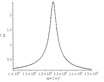
Experience and analysis [7] show that coupling decreases very quickly when distance between coils increases. That is why transformer coils are installed as close as possible.
In the apparatus described above, the resistive load is replaced by a capacitance C2. This new coupling
exhibits a resonance phenomenon at a certain frequency. This is visible by plotting induced voltage versus frequency of the current source, all other parameters remaining fixed (Figure 8).
1.5
0.5-1. X 10' 1. 1 X 10, 1.2 X 10-" 1.3 X 10 1.4 X 1 G' 1.5 X 10-o>=2 !tf
Figure 8: Voltage gain versus frequency, for a coupling coefficient k = 0.1. This figure was plotted from equations derived in section 4.1, where u2 = V.
At this frequency, called resonant or natural frequency, the power transmission is much more efficient. Thus, the distance between the coils can be substantially increased.
2.5.
Applications
This physical phenomenon can be advantageously used for contactless applications. We present two of the most important: RFID tags and wireless power. Both applications are used by ProTeqt. Before the deactivation of the lock, the product is recognized by its RFID tag, inside the package. Then, the principles of wireless power transmission will be used in order to increase the maximum distance of deactivation.
2.5.1. RFID
Nowadays lots of company make a massive use of automatic identification systems, or Auto-ID, for a large range of applications: inventory management, sales and purchase, payment, safety controls, communication ... The most widely used are the barcode and the smartcard. Among all the available solutions, RFID systems (for Radio Frequency Identification) have three major advantages: identification is passive, contactless and reconfigurable. Like smart cards, data is stored on an electronic data-carrying device, called the chip. However, RFID devices do not require physical contact between the chip and the reader. Instead, data exchange is achieved using electromagnetic field. The electromagnetic waves are
emitted and received through two coils (or antennas), one is connected to the chip and the other one is in the reader. The device made by the antenna and the chip is called transponder.
To maximize the power transmission and thus the working distance between the transponder and the reader, the resonant frequency of the system is used to convey information. Two kinds of systems can be distinguished: passive and active transponders. A passive transponder does not provide any energy and only receives it from the reader's magnetic field. This energy results in a change in the impedance of the transponder. This shifts the initial natural frequency of the system, which is detected by the reader. On the opposite, active transponders carry a battery. They can transmit their ID signal using their own energy source. The signal is sent either periodically or in the presence of an RFID reader. Passive transponders are more widely used, mainly because they are less expensive. The advantage of active transponders is that they work at higher distance [6].
2.5.2. Wireless Power
Wireless energy transfer is as old as alternating current [8]. The transformers are ubiquitous in most electronic devices and indeed in all electricity distribution network transfer energy by using mutual inductance. In recent years, wireless energy transfer for an array of applications has become an increasingly investigated use of resonant inductive coupling. A team of physicists at MIT has worked on this subject since 2005 [9,10]. They realized that resonant objects tend to couple, whereas off-resonant interaction remains extremely weak. Thus, energy transfer efficiency between two resonators increases with the coupling level between them. It is called non-radiative wireless energy transfer. In terms of energy transfer, non-radiative transfer is much more interesting than other solutions, such as radiative transfer (huge loss) or directed radiation modes (that requires uninterruptible line-of-sight). Some foreseen applications are:
" Charging portable electronic devices by placing it within the source field " Supplying power to mobile robots and machines in a factory
* Supplying power to internal medical device (pacemaker, medicine delivering devices ...)
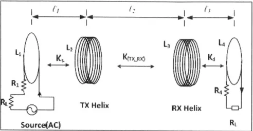
Over the years, several designs have been tested and refined. For now, the highest efficiency has been achieved with a four-coil apparatus: the power supply with an inductor, first resonator, second resonator, and the receiver with the device to power (e.g. a light bulb). A schematic of the system is given in Figure 9.
(. -bh. ~ L RL Source(AC)
*1
TX Helix 13 L4 Kd RX HelixFigure 9: Typical Strongly Coupled Magnetic Resonance (SCMR) System. TX is the transmitting helix. RX is the receiving helix. [11]
Resonant inductive coupling only happens between the two resonators. The transmitting helix is inductively coupled with the source loop. Similarly, the receiving helix is inductively coupled with the load loop. With this system, several promising achievements have been reached. It is able to provide more than 90% efficiency at 15 cm distance. At a distance of 2 m, it can achieve an efficiency of 40% for single receiver and up to 60% for multiple receivers. Recently, the research team, now a company called Witricity, introduced a repeater to extend the magnetic field further, and thus reach higher transfer distance. This repeater inserts another resonators in between the two previous ones (transmitting and
Chapter 3
LC Circuit Manufacturing
Proteqt had previously determined that an LC circuit with a resonant frequency in the range of xxxx would be necessary for distance activation. This circuit would be part of each device , and therefore must be compact enough to fit in the locking device and inexpensive enough to keep the device cost low. These requirements make the design and manufacture of this circuit critical to the success of this product. In this chapter we examine a variety of methods for making such a device.
3.1.
Inductor Manufacturing
An inductor, in its simplest form is a coil of wire used to resist a non-constant current flow [13]. It stores energy in a magnetic field created by current flowing through a coil. Inductors can come in many shapes and sizes. These parameters often affect inductor performance [14]. The magnetic field created by inductor is very dependent on inductor shape, whereas the intensity of the field is determined by the number of turns within the coil. For our application we are interested in designs that will permit an electromagnetic field extension through resonant coupling. Materials are especially important in inductors. The time required to establish a magnetic field is proportional to the coil resistance [13]. High current is desirable to quickly set up a magnetic field. Changing the linear length of the coil, or the coil's material properties can alter resistance, and therefore the field
[14]. High coil resistance will also result in heating, and therefore promotes energy loss.
For this project, three inductor-manufacturing methods were analyzed: chemical etching, coil winding and screen printing. After consulting ProTeqt's manufacturing partner, MeadWestVaco, winding was deemed the least expensive method to make coils quickly and repeatably. However, other methods may be considered for two reasons:
* If they can achieve better energy transmission between the primary and secondary coils, or " If they become more competitive in the near future.
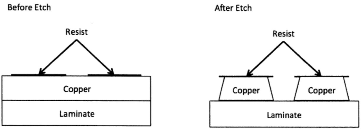
3.1.1. Chemical Etching
Chemical etching is a controlled material removal process that uses a resist to prevent portions of a material from being removed by a chemical etchant. Once the resist is removed, a desired pattern remains. The process at hand uses copper and a resist to etch a copper pattern.
Before Etch After Etch
Resist Resist
Copper Laminate
Copper Copper
Laminate
Figure 10: Schematic of a typical etching process.
Figure 10 explains how chemical etching works [15]. You will notice that the etchant removes material in two directions, not just vertically. That is, a slight angle is apparent in the final product because the etchant is in contact with that portion of the material after it passes beyond the resist. Finally, it's important to not that this is a chemical material removal process. Meaning the copper that is removed cannot be easily recycled, making the process as a whole, inefficient.
Etching allows for batch processing of inductors however, restricts coil designs to single layer, flat spiral coils. Economical etching is usually done in large batches of very thin materials. These materials are often on the order of 0.03mm thick [15]. As material thickness increases, time to etch increases. This property is inefficient in terms of processing energy. This directly impacts the production cost.
As material thickness decreases, resistance increases. This resistance restricts current flow through the material, and therefore increases the amount of voltage needed to create an electromagnetic field. The time requirement to etch thick pieces of copper (0.5mm) is about 5 minutes [16]. This however is not what limits the chemical etching process in terms of this application. The limiting factor is in the material costs. Copper is very expensive, and is only one of the materials used in the
process. Resist and the chemical etchant also need to be purchased, along with the many cleaning solutions used to remove the etchant.
3.1.2. Coil Winding
Coil winding is a process that bends a wire (usually radially) into a desired shape. This can be done manually or automatically, and many different winding patterns can be achieved. This process bodes well for inductor manufacturing because an inductor, in its most basic form, is a wound coil. Size and shape of the coil, and wire used to create the coil can impact the inductor performance. Wound coils can be formed into almost any desired shape including flat spiral, cylindrical, rectangular, etc. Wire geometry is often limited by market availability. Rectangular and circular cross sectional wire are most common. Wires are found most commonly in certain AWG gage sizes, which have a circular cross section. Diameters are fully customizable depending on the type of winding machine. Usually machines can operate using a range of wires. Automatic machines often integrate several functions including dispensing, winding, and cutting the wire. Machines can accommodate simultaneous coil winding, providing a batch process. Batch processing allows the machines to
produce coils at a high rate.
The cost of wire is very low compared to copper foils (used in etching). Wire is packaged as a large spool that is fed into the coil winding machine. Because the wire is continuous, there is almost no waste and the two ends of each coil are left exposed, ready to be soldered to the remaining capacitor.
3.1.3. Screen Printing
Screen printing is a highly integrated manufacturing process that can provide an entire LC circuit in one process. The process uses a mask that contains the circuit pattern. Conductive ink is then deposited on the mask, and the circuit is printed on the areas not protected. Silver and Aluminum are the most popular conductive inks used in this process. Dielectric materials can also be used to print capacitors. This is done in layers. First a conductive layer is deposited, followed by a dielectric, and finally another conductive layer. [17]
The flexibility of screen printing is similar to that of chemical etching. It is commonly used for making flat, flexible circuits. The deposited layers are very thin (40 micron), but can be built up in layers. Building layers requires more processing time, and is therefore less economical. The thin nature of screen printing causes inherently high resistance values. Capacitors are printed as large flat surfaces,
requiring a large amount of surface area. Spacing is also critical in screen printing. The silver ink does not have an insulating coating, so line spacing also requires more space. Like chemical etching, large batches can be printed at once. However, screen printing requires no post processing because the capacitor can be printed as part of the circuit. [17]
The screen printing process is new relative to processes like etching or winding. While the added flexibility and integrated components are great for circuit board design and manufacture, it is still a new processes, and therefore costly. Future developments are expected to lead to significant cost reduction, leaving it as a potential process for future manufacturing. [17]
3.2.
Capacitors
Capacitors are common electrical components used in many types of circuits. They consist of two conductive plates that are separated by a dielectric layer. This configuration allows capacitors to hold a charge. Capacitors come in many shapes and sizes due to their simple design (see Figure 11). Capacitors are made in extremely high volumes by expert manufactures. With their cost at $0.0074 per capacitor, ProTeqt will be purchasing capacitors to use within their circuit.
Al
AM
Figure 11: Typical shapes and sizes of capacitors.
Capacitor specifications usually include three key pieces of information: nominal capacitance and rated voltage. A capacitor will likely have these values printed on its side. A capacitor reading 1 pf
20% at 10V, for example, will have a nominal capacitance of 1 microfarad with a tolerance of ± 20% (0.8ptf - 1.2ptf). Throughout the life of the capacitor, it should not handle more than 100 volts, as that is the rated voltage.
3.3.
Soldering Techniques
Soldering is a method of joining two thin metals using a filler material. This filler material has a lower melting temperature than the two thin metal pieces, allowing the filler material to flow between, and bond to each of the thin metal pieces. The filler material is often made of tin and lead. Conductive properties allow soldering techniques to be prevalent in the electronics manufacturing industry, and especially circuit board manufacturing. Two common soldering methods are used in manufacturing today: robotic soldering and dip soldering.
Robotic soldering often uses a robot or other automation to control temperature and the feed rate of the filler material. Sophisticated control systems are used to gain a high level of precision over soldering processes. Robotic soldering often requires auxiliary tooling or methods of positioning and orienting components before they can be soldered.
Dip soldering is used more extensively for circuit board manufacturing. This process is used to solder several components simultaneously. Leads from electrical components protrude through the bottom of the printed circuit board. These are dipped into a lead-tin bath, where the solder then solidifies upon removal. [18]
Chapter 4
Physics of the Problem and Theoretical Analysis
This short chapter introduces some theoretical analysis of the resonant inductive coupling. In section 4.1, a formula is derived to find the secondary current with respects to the characteristics of the two circuits and the coupling coefficient. Then, in section 4.2, a theoretical optimal coil is proposed in order to limit the range of the experimental field.4.1.
Analysis of the Coupling
in order to provide a better understanding of the problem, a theoretical analysis is proposed. The following calculations are directly adapted from [7]. First of all, we consider two spiral coils that are inductively coupled. The inductances of these coils are respectively Ll and L2. The primary coil is connected to a source of voltage E that generates a current il:
E = Ee j2TfO t (4.1)
= Ile j27fot (4.2)
where fo is set to 220 kHz, the working frequency of the tablet
The secondary coil is connected to a capacitance C2.Furthermore, the two coils are considered as a perfect inductance (resp. Ll and L2) in series with a resistance (resp. R1 and R2). This resistance is the
resistance of the coil's copper wire. It is assumed that the total resistance of each circuit only consists of the coil's resistance. Figure 12 shows the diagram of the apparatus.
R, R2
E
L , L2 C 2
i2
As explained in section 2, the current passing through the primary coil creates a magnetic field, which induces a voltage V2 in the secondary circuit. This voltage.depends on the mutual inductance (M) that
represents the quality of the coupling.
dil
V2 = M dt (4.3)
Reciprocally, the secondary circuit then induces a voltage V1in the primary circuit:
di2 V, = M
-dt where i2 is the current passing through the secondary circuit.
(4.4)
As a result, the system is entirely defined by the two following relationships (given in complex notation):
(R1+ j2mfOL1)ij + j2rfo Mi2 = E (4.5)
and
(R2+j ( 2wfoL2 - (4.6)
2 )) 2 ++j2foM~i = 0
27TfoC2-In order to simplify the equations, we introduce the impedance of each circuit:
Z, = R1 + j2wfOL (4.7)
Z2 = R2 +j 2wfOL 2 - (4.8)
2 7fo C2
Finally, combining equations (4.5) and (4.6),
. j2wfOME
- Z - Z2 + (2wf0)2M2 (4.9)
27rfo = (4.10)
L2 C2
Moreover, the mutual inductance verifies M = k L1L2, with 0 k 1 [6].
So, equation (4.9) becomes
jE - k
'- C2 (4.11)
- R2(Rj+jL1/ L2C2)+k2L1/C 2
Equation (4.11) gives an accurate idea of the physics of the problem. However, the coupling coefficient k is particularly difficult to evaluate. Some experimental methods have been developed to do so. The reader can refer to [7]. For the purpose of this thesis, the knowledge of k did not appear to be relevant. However, these equations give the general shape of the induced current versus the magnetic field frequency. Thus, they can be fitted to experimental data.
4.2.
Theoretical Optimization of the Coil
We can define coil efficiency as the amplitude of the magnetic field it can generate to heat up the enabler. The magnetic field is proportional to the current across the coil. Thus, we want to optimize the geometric characteristics of the coil, especially gage size and number of turns, in order to maximize induced current. In equation (4.11), the secondary current is a function of parameters that depend either on primary or secondary coil, or even on both, such as the coupling coefficient k. To simplify the expression of i2, it is assumed that the primary coil generates a constant magnetic field, whatever the
characteristics of the secondary coil. This magnetic field is vertical along the axis of the primary coil. At 1 inch above the center of the coil, its magnitude is B. The induced voltage in the secondary circuit is now
N
d B
V2= ai - (4.12)
-d t
i=1
where aj is the area enclosed in the ith loop of the coil and N is the number of turns of the coil.
For ease of notation, we introduce the geometric factor A = EN=ja. The defining relationship of the secondary circuit is now
dB
Z 2 + A -- dt = 0 (4.13)
with Z2 the impedance of the secondary circuit (see eq. 4.8) and i2 the current passing through it.
Assuming B = Be 2Jfot, equation (4.13) becomes
Z2' i2 +j2wfoAB = 0
.2TfO AB
i2 2fA
(4.14)
If the secondary circuit is tuned to resonate at fo, then Z2 = R2, so
.j2TfO AB
_2 = R2 A (4.15)
And the modulus of i2 is
2TfO AB
12= R2 (4.16)
Only A and R2 depend on the secondary coil geometry. They can be determined from two characteristics
of the coil: the wire gage and the number of turns. A spreadsheet has been written to evaluate the geometric factor and the resistance of the secondary coil, from the wire gage and the number of turns. The detail of this spreadsheet is given in appendix A.
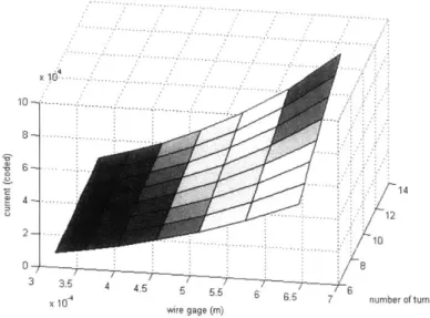
Finally, the amplitude of the current in the secondary circuit is plotted with respects of the gage size and number of turns of the coil. As the value of the magnetic field amplitude was not known, the plot actually represents 12/BI .
- 12
2 -- 10
06
x 1 6 .65 7 number oftumn:
10 wire gage (in)
Figure 13: Current in the secondary circuit (coded unit) versus the number of turns and the gage size
Figure 13 shows that the most efficient coil has high number of turns and large wire gage. This conclusion has several limitations and must not be generalized outside the boundaries of the actual problem:
* The secondary coil must be significantly smaller than the primary one in order to assume that the coupling does not affect the primary magnetic field and that the magnetic field is constant through the secondary coil.
* There is no evidence that this conclusion would remain true at higher frequency than 500 kHz
-1 MHz
Before considering the geometric constraints inside the lock, this theoretical result is compared to a set of experiments conducted on different coils.