Semiconductor saturable absorber mirror structures with low saturation fluence
Texte intégral
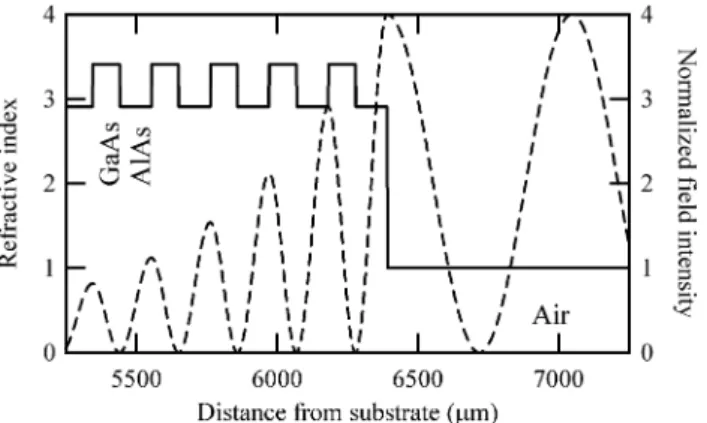
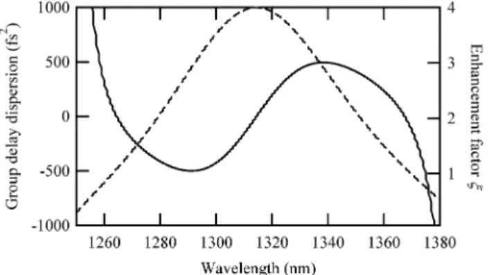
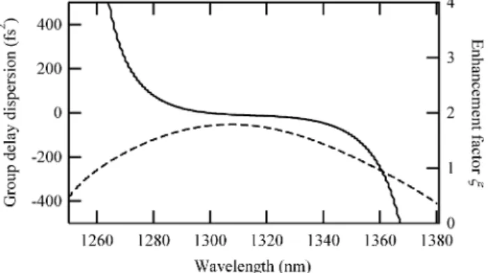
Figure
![Figure 11 shows the measurement of nonlinear reflectivity as a function of fluence incident on the samples [27], fitted](https://thumb-eu.123doks.com/thumbv2/123doknet/14867578.638214/5.892.453.806.76.312/figure-measurement-nonlinear-reflectivity-function-fluence-incident-samples.webp)
Documents relatifs
Pour l'obtention d'un tel diplôme sont notamment pris en considération les unités obtenues au second cycle du secondaire, parmi les matières à option des programmes de
dependence of absorption coefficient 03B1 and refractive index n on the intensity of incident light are studied near the exciton resonance. The non-boson behaviour
We study the wave absorption efficiency of a 3-DOF cylindrical buoy under varying PTO coefficients, mass density of the buoy, and incoming wave heights using the FD/BP methodology..
In deriving parameters for potentials used in defect studies, we have generally used empirical methods [6,7] : variable parameters of our lattice model have
Now both types of vacancy can ionize to give free holes and electrons ; however, as both our own calculations [12] and Kroger's ana- lysis [15] show, electrons
These are: (i) forn~ulat~ion of a set of ordinary differential equations for the cletuned case, by illearis of the uniform field approximation; (ii) an
The temperature variations of the domain width and the domain shape as well as the critical temperature essentially depend on the thickness of the examined crystal..
A new system, consisting of a double channel Fabry Perot etalon and laser diodes emitting around 780 nm is described and proposed to be used for air refractive
