Effect of intergranular glass films on the electrical conductivity
of 3Y-TZP
M. Godickemeier, B. Michel, A. Orliukas, P. Bohac, K. Sasaki, and L. Gauckler Nichtmetallische Werkstoffe, ETH Zurich, CH-8092 Zurich, Switzerland
H. Heinrich, P. Schwander, and G. Kostorz
Institut of Applied Physics, ETH-Zurich, CH-8093 Zurich, Switzerland H. Hofmann and O. Frei
Alusuisse Lonza Services AG, CH-8212 Neuhausen, Switzerland (Received 3 June 1993; accepted 11 January 1994)
The electrical conductivity of 3Y-TZP ceramics containing SiO2 and AI2O3 has
been investigated by complex impedance spectroscopy between 500 and 1270 K. At low temperatures, the total electrical conductivity is suppressed by the grain boundary glass films. The equilibrium thickness of intergranular films is 1-2 nm, as derived using the "brick-layer" model and measured by HRTEM. A change in the slope of the conductivity Arrhenius plots occurs at the characteristic temperature Tb at which the macroscopic grain boundary resistivity has the same value as the resistivity of the grains. The temperature dependence of the conductivity is discussed in terms of a series combination of RC elements.
I. INTRODUCTION
Thin intergranular glass films which are composed of SiO2, A12O3, and Y2O3 are formed in Y-TZP ceramics
at high sintering temperatures.1"7 They promote sintering
of the starting powders as well as grain growth during the post-annealing process and affect the electrical and mechanical properties of Y-TZP ceramics.8"11 It has been
shown that the equilibrium film thickness is limited to about 1-2 nm,4'12'14 and excess amounts of glass
segregate in grain triple junctions, in pores, and on the surface of the specimens.4'5'11 The equilibrium width of
intergranular films depends on the corresponding inter-facial energies and on the viscosity of the glass phase at the temperature of sintering or post-annealing.15'16 A
surplus of A12O3 is proposed to act as a scavenger for
SiO2, removing it from grain boundaries.17-18 The glass
phase can also be partially squeezed out from the grain boundaries to three grain pockets by applying a com-pressive stress.19 Accordingly, in hot-pressed specimens
of Y-TZP at 1823 K some "clean" grain boundaries were observed, which did not contain any detectable intergranular phase.16
The Arrhenius plots [Iog(cr7) vs l/T] of the total (dc) conductivity of zirconia-based solid electrolytes often exhibit a change of slope at 800-1200 K, owing to a decrease in activation energy at high temperatures.20"22
Rather controversial explanations for the origin of this curvature of the Arrhenius plots have been given in the literature.23"30 The majority of studies suggests that in the
low-temperature region immobile associated complexes, such as [YZ rVo]', are formed between extrinsic oxygen
vacancies and oppositely charged dopant ions. The ther-mal dissociation of these complexes would require a supplementary energy in addition to the activation energy for the simple migration of "free" charge carriers.23"26
According to this concept, three general stages of the ionic conductivity are proposed to exist in solid electrolytes as a function of temperature.27'31 The first
bend in the Arrhenius curve occurs on cooling from the high temperature "intrinsic stage I" to the "extrinsic-dissociated stage II" at which all extrinsic charge carriers are claimed to be mobile. The intrinsic stage exhibits a higher activation energy that is necessary not only for the migration but also for the formation of intrinsic charge carriers. At the transition temperature I —> II, the concentration of thermally activated intrinsic charge car-riers becomes equal to the total concentration of extrinsic charge carriers generated by doping. Another bend in the Arrhenius plot at lower temperatures is assumed to occur from the extrinsic-dissociated stage II to the "extrinsic-associated stage III". Since the activation energy of the low-temperature stage III includes an additional energy for the dissociation of defect complexes, it is again higher than the activation energy of the middle stage II, which corresponds to the energy for the migration of free extrinsic charge carriers only. At the temperature of the second transition (II —» III), the concentration of thermally dissociated, "mobile" extrinsic charge carriers is supposed to be equal to the concentration of extrin-sic charge carriers which are still associated and "im-mobile". Supposing association energies of 0.2-0.5 eV, Nowick and Park27 have calculated the temperature at
M. Godickemeier et at.: Effect of intergranular glass films on the electrical conductivity of 3Y-TZP
which a half of the total amount of extrinsic oxygen vacancies would be free. They suggested this tempera-ture to be the lower "break point temperatempera-ture" of the Arrhenius plots.
Other authors have interpreted the slope change of Arrhenius plots (stages II to III) to be due to changing from the volume-controlled conductivity of the grains, prevailing at high temperatures, to the grain-boundary-controlled conductivity at low temperatures,28"30 due to
microcracking,21 phase transformation,28'32 or even as a
mere artifact of the experimental technique.33
A formation of dopant-vacancy associates in the proposed "extrinsic-associated range (III)" was claimed to reduce the concentration of "free" charge carriers in stabilized zirconias with increasing dopant con-tent.2334"36 Assuming associated defect complexes,
Weller and Schubert26 have questioned the current
ac-cepted values of intragrain bulk conductivities and their activation energies obtained by impedance spectroscopy measurements and proposed a revision of the classical interpretation of this widely used experimental meth-od.28-37"39 On the other hand, no difference between
"mo-bile" and "immo"mo-bile" lattice defects was found in the studies of Orliukas et a/.,40 Casselton,41 and
Anantha-padmanabhan et al.42
To explain the blocking effect of the grain bound-aries, two models, in terms of an electrical connec-tion of the bulk and the segregated grain boundary material either in series or parallel, are given in the literature.8'9'14-37-43'44 According to the first, "brick layer"
or series model,8'9'20 conducting grains are separated by
a continuous film of a less conducting grain-boundary phase. The second, "easy path" or parallel model,45-46
assumes only a partial blocking of the current path due to a discontinuous distribution of an insulating phase between conducting grains.
In the present work the intergrain relaxation of the ionic conductivity has been studied by complex impedance spectroscopy on 3Y-TZP specimens contain-ing different amounts of the grain boundary glass phase. The purpose of this study was to clarify the relation-ship between the chemical composition of the starting material which determines the amount of the inter-granular phase and the electrical properties of 3Y-TZP ceramics and to provide a better understanding of the bend in Arrhenius plots of total conductivity observed in zirconia-based solid electrolytes at 800-1200 K.
II. EXPERIMENTAL
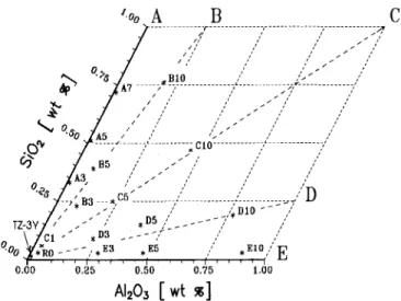
The compositions of the investigated 3Y-TZP sam-ples are shown, with respect to their SiO2-Al2O3
con-tent, in Fig. 1. The samples lie along the lines A, B, C, D, and E, which correspond to the SiO2/Al2O3
ratios of 1/0, 4 / 1 , 1/1, 1/4, and 0 / 1 , respectively. The
B
B1°
C10 ' ' ,'' •' *D5 A - - - " ' " , ' ' ' D3 '*
E10/ E
/
0.00 0.25 0.50 0.75 1.00AI
20
3[ wt %]
FIG. 1. The compositions of 3Y-TZP samples with respect to SiO2
AI2O3 impurities.
total amount of both oxides is given approximately in tenths of a weight % by the sample number and varies from about 0.1 wt. % for the C-l sample to 1 wt. % in samples B-10, C-10, D-10, and E-10. The coprecipitated 3Y-TZP powder without impurity additions has been considered as the reference (sample R-0). For com-parison, a sample from the pure commercial powder TZ-3Y (Toshoh Corporation, <0.005 wt. % SiO2 and
<0.002 wt. % A12O3), which is designated as TZ-3Y,
as well as a very contaminated sample F-46 containing 4.6 wt. % of both impurities in total have also been investigated.
All 3Y-TZP sintered specimens were prepared using coprecipitated ultrafine powders. The SiO2 and A12O3
impurities were introduced as SiCl4 and A1C13 into the
solution of ZrOCl2 and YC13 before the wet-chemical
precipitation. The only exception is the sample F-46, which was prepared by mixing of the reference powder R-0, calcined at 1023 K, with a fine SiO2 powder
(Aerosil OX50, Degussa) in an attritor mill. All other coprecipitated powders were calcined at 1223 K for 8 h. The calcined powders have specific surface areas between 11 and 36 m2/g. Their chemical analysis is
shown in Table I.
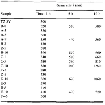
The starting powders were uniaxially cold pressed at 100 MPa and sintered for 1 h in air at 1773 K. The density of all sintered samples was >96% of the theoretical value. The ceramic microstructures were re-vealed by thermal etching of polished specimens at 1720 K for 30 min. Only the tetragonal crystalline phase was detected by x-ray diffraction after sintering. The average linear grain size parameter, / (see Table II), was determined as the mean intercept length on SEM photo-micrographs (JEOL, JEM-6400) by the linear-intercept method.47'48 It varies in the range of 300 nm to 430 nm.
M. Godickemeier et al.: Effect of intergranular glass films on the electrical conductivity of 3Y-TZP
TABLE I. Chemical composition of Y-TZP powders.
Sample TZ-3Y R-0 A-3 A-5 A-7 B-3 B-5 B-10 C-l C-5 C-10 D-3 D-5 D-10 E-3 E-5 E-10 F-46 SiO2: A12O3 ratio 2.50 > 1 > 3 3 > 5 1 > 7 2 2.56 4.88 4.00 2.00 1.09 1.04 0.39 0.38 0.25 <0.11 <0.06 <0.03 2.23 SiO2 <0.005 0.03 0.33 0.51 0.72 0.23 0.39 0.76 0.06 0.25 0.47 0.09 0.15 0.19 <0.03 <0.03 <0.03 3.15 A12O3 <0.002 <0.03 <0.01 <0.01 <0.01 0.09 0.08 0.19 0.03 0.23 0.45 0.23 0.40 0.77 0.28 0.47 0.89 1.41 Y2O3 (wt. %) 5.140 5.33 5.41 5.38 5.40 5.23 5.32 5.21 5.38 5.25 5.33 5.35 5.52 5.41 5.31 5.27 5.21 6.62 Na2O 0.023 0.08 0.04 0.05 0.05 0.01 0.01 <0.01 0.02 0.04 0.03 0.03 0.04 0.02 0.01 0.03 0.03 0.07
cr
<0.01 0.01 0.01 0.07 0.02 0.01 0.01 <0.01 0.13 0.01 0.01 0.01 0.01 0.01 0.01 0.01 0.01 0.01 2 imp. 0.10 0.15 0.39 0.64 0.80 0.34 0.49 0.97 0.24 0.53 0.96 0.36 0.60 0.99 0.33 0.54 0.96 4.64 BET (m2/g) 15.2 11 18 21 24 17 19 21 17 20 18 21 19 19 16 15 17 36Complex impedance spectroscopy at alternating fields of variable frequency37"39-45 has been used to
distinguish between the intragrain and the grain boundary contribution to the charge transport. The total impedance of the ceramic specimens originates from the impedance contribution of the grains and from interfacial effects on grain boundaries and electrodes. A simplified equivalent circuit consists of three resistors in series, each shunted by a capacitor in parallel.
The complex impedance measurements using a PC-controlled HP Precision LCR meter 4284A were carried
TABLE II. Linear average grain sizes of annealed 3Y-TZP samples.
Grain size / (nm) Sample TZ-3Y R-0 A-3 A-5 A-7 B-3 B-5 B-10 C-l C-5 C-10 D-3 D-5 D-10 E-3 E-5 E-10 F-46 Time: 1 h 300 320 320 360 350 430 380 390 340 380 380 380 430 380 390 410 410 300 5 h 510 440 810 510 580 1010 620 470 10 h 580 560 960 660 810 1280 1060 720
out between 500 and 1200 K in air, on sintered cylindri-cal samples 10 mm in diameter and 1-2 mm thick, using the two-point probe technique. The frequency range was 40 Hz to 1 MHz. Platinum electrodes were painted on the specimens by applying a conductive platinum paste (Demetron 308A) and sintered onto the surface at 1073 K. The temperature was controlled to ± 2 °C.
III. RESULTS AND DISCUSSION A. Impedance spectroscopy
An example of the frequency dependence of the real part of the specific electrical impedance, p' ~ Z' •
L/A, where Z' = UR/IR is the real part of the complex impedance Z = Z' + iZ", L is the sample length, and
A the electrode area, is shown in Fig. 2 (sample E-10).
10000
10 100 1000 10000 100000 1000000
f[Hz]
FIG. 2. Grain, grain boundary, and electrode dispersions of the real part of complex specific impedance (sample E-10).
M. Godickemeier ef a/.: Effect of intergranular glass films on the electrical conductivity of 3Y-TZP
The relaxation dispersions of individual impedance con-tributions (grains, grain boundaries, and electrodes) shift toward higher frequencies with increasing temperature. This indicates that these dispersions are thermally ac-tivated. Usually it is not possible to observe all three dispersions simultaneously, due to a limited frequency range used in this study (40 H z - 1 MHz). At temper-atures below 500 K only the grain dispersion can be seen at high frequencies.40 The grain boundary and
the electrode dispersion are too slow to be detected at this temperature. In the medium temperature range (500 K - 8 0 0 K), we can observe two dispersions, that of the grains and that of the grain boundaries. Finally, above 800 K the intragrain dispersion shifts out of the frequency window and the sluggish dispersion due to the slower electrode processes becomes visible.
In Fig. 3 the frequency dependence of the specific imaginary impedance contribution, p" = Z" • L/A, is shown. From this figure the individual dispersion regions of grains, grain boundaries, and electrodes can be seen more distinctly.
The complex impedance data can be displayed in the complex impedance plane with real part p' as the ab-scissa and the imaginary part p" as the ordinate (Cole-Cole diagram). A typical complex impedance spectrum of 3Y-TZP (sample E-10) at a medium temperature of 596 K is shown in Fig. 4. Since the time constants (r = RC) of individual RC-elements differ by orders of mag-nitude, individual semicircles of the grains and that of the grain boundaries can clearly be distinguished in this temperature range. The real specific impedance sections between the distinct minima in the imaginary part p" reveal the macroscopic specific resistivities of the grains (p'G) and the grain boundaries (P'GB), respectively. The macroscopic specific resistivity of the grain boundaries is equal to the difference between the total (dc) spe-cific resistivity of the sample (p r) and the macroscopic
1200
0 500 1000 1500 2000 2500
P' [Ohm m]
FIG. 4. Complex impedance diagram at 596 K (sample E-10).
specific resistivity of the grains: PGB = PT ~ Pa- More-over, from the maximum of imaginary impedance p" at the top of each semicircle, the relaxation frequency w of the corresponding process can be determined from the relation COT = 1, where co = 2irfR, is the angular frequency [rad- s"1], /R the corresponding frequency of
the applied electrical ac-field [Hz], and T = RC the time constant of the relaxation circuit.
B. Microstructure
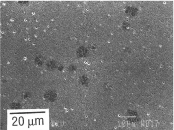
The microstructures of the sintered 3Y-TZP speci-mens reveal for samples TZ-3Y, R-0, C-l, D-3, and the whole E series only very small amounts of the glass phase in triple points. On the other hand, all samples of both the B and C series as well as samples D-5 and D-10 contain large glass pockets surrounded by cubic grains (Fig. 5). Segregations of the glass phase at triple points can also be observed in samples of the A series containing silica additions without alumina.
1000 100 i E
I
O 0.1Grain boundaries Grain
Electrodes
•k
10 100 1000 10000 100000 1000000
f[Hz]
FIG. 3. Frequency dependence of imaginary part of complex specific
M. Gddickemeier et al.: Effect of intergranular glass films on the electrical conductivity of 3Y-TZP
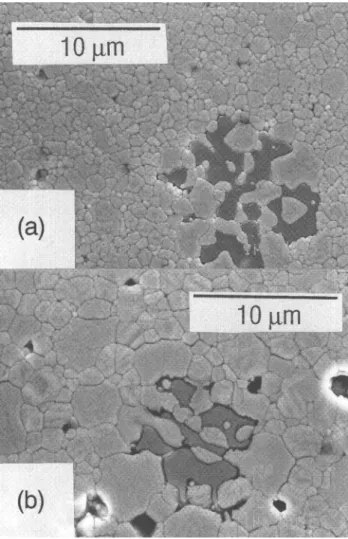
The annealing of selected samples at 1773 K for 5 and 10 h at 1773 K caused the separation of the tetrago-nal and cubic phase and a gradual grain coarsening. The linear average grain sizes, /, are given as a function of annealing time in Table II. When the tetragonal grains reach a critical size, the tetragonal zirconia transforms on cooling to the monoclinic phase. This phase transition, which occurs in specimens annealed longer than 20 h, is accompanied by the formation of numerous microcracks and causes an abrupt increase of the grain boundary resistivity due to the partial blocking of the conduction path by microcracks. From Fig. 6 the development of the microstructure around a glass pocket during annealing of the B-3 sample is visible.
High resolution electron micrographs (Philips CM 30 at 300 kV, super twin lens, Cs = 1.1 mm, LaB6 cath-ode) of grain boundary regions revealed in all samples homogeneous amorphous films about 0.5-2 nm thick. No "clean" grain boundaries without intergranular phase have been observed, even in the E series. In 3Y-TZP samples containing a large amount of the glass phase
l O u m
(a)
I.' . i. .— 7
* . . * • * , - - - ' ' 1 >(b)
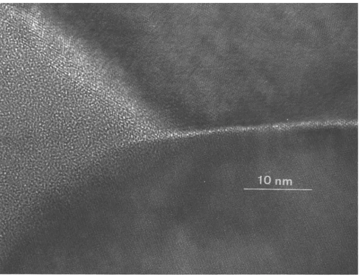
(C-5, B-10), the excess of the glass phase accumulates at three-grain pockets and at the surface. Figure 7 shows a three-grain junction area of the sample C-10 and an intergranular glass layer about 1-2 nm thick. The EDX and PEELS (parallel electron energy loss spectroscopy) analysis of the glass in triple grain junctions and in large multi-grain pockets showed that the segregated amor-phous phase contains oxides of all four elements, Si, Al, Y, and Zr, except that in samples with both low SiO2/Al2O3 ratio and low total impurity content no Y
and Zr, and in the A series also no Al, could be detected. The glass phase in pockets of the C-10 sample consists of 42 wt. % SiO2, 22 wt. % A12O3, 21 wt. % Y2O3, and
15 wt. % ZrO2 (Fig. 8). This composition of the grain
boundary phase is in a good agreement with the results of other authors,1'3'5'14'16 which also showed the presence
of Si, Al, Zr, and a high concentration of Y.
C. The "brick layer" model
To analyze the electrical conductivity of a ceramic material in which the intergranular phase is present as a three-dimensional connected network of continuous films, the brick layer model can be used.8'9'14'49'50
Ac-cording to the brick-layer model, it is assumed that the bulk material consists of conducting grains, cubes with an edge length a, separated by a thin homogeneous grain boundary layer of low conductivity of the thick-ness <5gb. Since <5gb < a and aGB ^ &G, the parallel conduction along the grain boundaries can be neglected. The equivalent electrical circuit consists then of a simple series combination of two RC-elements (grain and grain boundary). The total (dc) resistance of the sample, RT = RG + RGB, is the sum of the resistance of grains RG and grain boundaries RGB. Usually the macroscopic specific conductivities a'T, <r'G, and aGB are calculated from resistivity values, using the relation:
a[ = l/p[= l/(RrLT/AT),
where LT = LG + LGB = n{a + 8GB) is the total length of the sample between the electrodes, n = LT/a is the number of grain boundaries perpendicular to the current direction, and AT = AG + AGB is the total cross-section area of the sample. Since LGB/LT = Sgb/(a + <5gb), it can easily be shown that the length fraction of
grain boundaries LGB amounts to LT • 8gb/(a + <5gb) = LT ' Sgb/a and that of grains LG to LT • a/{a + Sgb) = LT. For the cross section of the current path through the area fractions of grains AG, we obtain:
AG = AT • a2/(a + §g b/ 2 )2 = AT • a/(a + <5gb) = AT.
FIG. 6. Microstructure development during annealing at 1773 K (sample A-5): (a) 10 h and (b) 30 h.
Omitting the parallel grain boundary conduction path along the length of the sample, the microscopic specific
M. Godickemeier et at.: Effect of intergranular glass films on the electrical conductivity of 3Y-TZP
FIG. 7. HREM of a triple-point junction and an intergranular glass film (sample C-10).
300 g 200 100 + 0 2 100 SEC 10 12 14
FIG. 8. EDX analysis of the glass phase segregated in a large pocket (sample C-10).
Zr
16 18 20
M. Godickemeier ef at.: Effect of intergranular glass films on the electrical conductivity of 3Y-TZP
conductivity of the grain and grain boundary material at low contents of glass phase (a > <5gb) is then given by,
aG = and aGB = a'GB • Sgb/a (1)
In order to eliminate the size effect of ceramic grains, the macroscopic specific grain boundary resistivities, p'gb = ^GB " AT/LT, have been converted to the normalized macroscopic resistivities per unit area of the grain bound-ary surface,51 rGB, according to the relation,
= P
rGB =
where a = 1.5/ is the corresponding cube edge length derived from the linear average grain size of the ceramic sample, /.47>48 The microscopic specific resistivity of the
grain boundary glass material, pGB = RGB • AT/LGB, is
then the ratio of the macroscopic resistivity per unit area rGB to the grain boundary thickness <5GB(/°GB =
''GB/SGB)- In case the thickness of the intergranular glass films is known, the microscopic permittivity of the grain boundary material, eGB, can also be derived from
the macroscopic grain boundary capacitance, CGB (see
Table III), according to the relationship:
Using the "brick layer" model,8-14 we obtain:
eGB = CT-GB • 8GB/(a2irfR€0) = CGB/e0 • (8GB/a), (2) where e0 = 8-85 pF/m is the permittivity of free space.
Table III summarizes our experimental results on the electrical properties of grain boundaries at 673 K.
Figure 9 shows the relationship between the normal-ized grain boundary resistivity rGB at 673 K and the
content of total impurities. Neither the total impurity concentration nor the increasing SiO2 content alone
are responsible for the increase of the grain boundary resistance. Much more important is the combination of the appropriate impurities which determines the amount of the glass phase, especially the SiO2/Al2O3 ratio (see
Table I). The normalized grain boundary resistivity of both series A and E, to which only one of the glass components, SiO2 or A12O3, has been added, remains
almost as low as the pure standard material (R-0) even at high total additive levels. On the other hand, the B, C, and D series containing both SiO2 and Al2O3 exhibit
relatively high normalized intergrain resistivities as soon as the total additive content exceeds a threshold value of about 0.3-0.5 wt. %. Already 0.2 wt. % of silica leads to a dramatic increase of the normalized grain boundary resistivity if enough alumina is present in the sample. The resistivities remain then constant at higher im-purity levels.
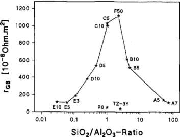
Figure 10 shows the dependence of normalized re-sistivity of intergrain films on the SiO2/Al2O3 ratio.
The highest resistivities are found in samples containing both impurities in the SiO2/Al2O3 ratio of 1/1 to 3 / 1 .
Pure silica does not melt at the sintering tempera-ture. Additional oxides, especially alumina and yttria, are necessary for the formation of the liquid phase at this temperature. We can assume that the appropri-ate amounts of Y2O3 and ZrO2 are supplied by the
matrix to form the glass melt. The glass-forming re-gion of the ternary SiO2-Al2O3-Y2O system,52'53 which
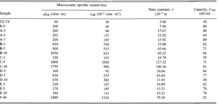
TABLE III. Relevant parameters of the grain boundaries in 3Y-TZP samples at 673 K. Macroscopic specific resistivities
Sample PGB (ohm • m) ohm • m2)
Time constant, r (10-6 s) 3.98 7.96 17.67 15.92 15.92 53.00 63.66 69.23 18.78 127.32 106.16 10.66 63.66 31.83 19.89 13.21 13.21 79.58 Capacity, CGB (nF/m) 50 80 88 64 80 62 71 66 59 71 61 66 77 48 62 78 74 32 TZ-3Y R-0 A-3 A-5 A-7 B-3 B-5 B-10 C-l C-5 C-10 D-3 D-5 D-10 E-3 E-5 E-10 F-46 100 200 250 200 850 900 1050 320 1800 1750 160 830 670 320 170 180 2480 36 48 96 135 105 548 513 614 163 1026 998 91 535 382 187 105 111 1116
M. Godickemeier et al.: Effect of intergranular glass films on the electrical conductivity of 3Y-TZP E .c O 10 O m a 1200 1000 800 600 400 200 0 -B 3 / / D3 **~ R0 • A C5 •t— / / D5 — - • ^=d B5 / ' A5 9 E5 • ~ * -A7 • C10 B10 - • D10 E10 0.0 0.2 0.4 0.6 0.8 1.0 Total Impurities [wt%]
FIG. 9. Normalized grain boundary resistivity at 673 K as a function of impurity content.
AI.O, sio, L 0
0 10 20 30 40 50 60 70 80 90100 wt% SiO2 —
FIG. 11. Region of glass-forming melts in the SiC>2-system52 at 1773 K. - 100 - 9 0 - 8 0 - 7 0 - 6 0 - 5 0 - 4 0 - 3 0
6*
CM -20is liquid at the sintering temperature of 1773 K, is shown in Fig. 11. The arrows outgoing from the binary SiO2-Al2O3 subsystem mark the compositional lines on
which our sample series are located.
Assuming total yttria saturation from the Y-TZP matrix, only the appropriate SiO2/Al2O3 impurity ratio
determines the final composition of the intergranular glass phase. The melt composition lowest in A12O3 lies
in this ternary system in the sketched part of the phase diagram at about 10 wt. % A12O3 and 50 wt. % SiO2 (a
in Fig. 11). This glass composition is in equilibrium with solid SiO2. For the A series containing SiO2 additive
only, the amount of the ternary glass phase of composi-tion a lies at ten times their A12O3 impurity-content in
wt. % (10 wt. % A12O3). For the B series, the content of
glass of composition designated with a corresponds to twice the SiO2 concentration in wt. % (50 wt. % SiO2).
0.1 1 10
SiO2/AI2O3-Ratio
FIG. 10. Normalized grain boundary resistivity at 673 K as a function of the SiO2/Al2O3 ratio.
On the other side of the diagram, the Al2O3-rich melt
composition which is in equilibria with solid A12O3 is
at 35 wt.% A12O3 and 35 wt. % SiO2 (b in Fig. 11).
The alumina rich series C, D, and E will form glass of composition b in amounts corresponding to about three times their SiO2 concentration in wt. % (35 wt. % SiO2).
The calculated glass contents of all specimens in wt. % are given in Table IV. \
Although the liquidus of the quaternary S i O2
-A l2O3- Y2O3- Z r O2 system has not yet been elucidated,
we can expect an analogous region of glass melts at 1773 K, lying between 10 wt. % A12O3 and 50 wt. %
SiO2 on the SiO2-rich side and 35 wt. % A12O3 and
35 wt. % SiO2 on the Al2O3-rich side of the quasi-binary
edge. This assumption is supported by EDX analysis of glass areas in the triple grain junctions showing systematic variations of the glass phase composition in function of the SiO2/Al2O3 ratio.
From the densities of the bulk 3Y-TZP material and of the S i O2- A l2O3- Y2O3 glass compositions, we
can determine the volume content of the glass phase using the following simplified equation, valid for small concentration of the glass:
Vol. % glass = wt. % glass • DTZp/Dgiass,
where DTZ? = 6.08 g/cm3 is the theoretical density of
3Y-TZP and £>giass the density of the glass phase.
The density of the glass phase depends on its compo-sition, and varies especially with the yttria content. For the ternary S i O2- A l2O3- Y2O3 glass of composition a
(see Fig. 11) with a content of 10 wt.% alumina, the density is known54 to be 3.2 g/cm3; for the alumina
rich glass b the density54 is 3.5 g/cm3. The appropriate
M. Godickemeier ef a/.: Effect of intergranular glass films on the electrical conductivity of 3Y-TZP
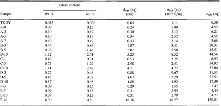
TABLE IV. Derived specific properties of intergranular glass films at 673 K.
Glass content Sample TZ-3Y R-0 A-3 A-5 A-7 B-3 B-5 B-10 C-l C-5 C-10 D-3 D-5 D-10 E-3 E-5 E-10 F-46 Wt.% 0.015 0.09 0.10 0.10 0.10 0.46 0.78 1.52 0.18 0.75 1.41 0.27 0.45 0.57 0.09 0.09 0.09 6.30 Vol. % 0.026 0.15 0.19 0.19 0.19 0.86 1.46 2.61 0.31 1.29 2.42 0.46 0.77 0.98 0.15 0.15 0.15 10.8 " L I D V1-" (nm) 0.04 0.24 0.30 0.34 0.33 1.87 2.82 5.23 0.53 2.48 4.71 0.88 1.67 1.88 0.29 0.31 0.31 18.16 0GB (eq) (10^ S/m) (eq) 1.11 5.00 3.13 2.52 3.14 3.41 5.50 8.52 3.25 2.41 4.72 9.67 3.29 4.93 1.55 2.95 2.79 16.27 0.50 4.52 6.21 4.55 5.68 20.31 15.51 44.56 6.93 34.92 57.00 11.51 22.51 17.39 3.47 4.44 4.21 130.81
each composition from the amount of SiO2 and A12O3
impurities and is given in Table IV.
Figure 12 shows the normalized grain boundary resistivity at 673 K as a function of the calculated glass content in vol. %. At glass contents of more than 1 vol. %, the intergranular resistivity remains approx-imately constant (sample series B, C, and D). This indicates that an equilibrium thickness of the intergranu-lar film has already been achieved and the further excess of the glass phase segregated at triple grain junctions and on the surface of the specimens.
From the volume fraction of the glass phase and the average linear grain size / (Table II), the
equiva1200 1000 800 600 400 200 0
-/f\
/I
E*A *D3 •-•RO C5 / / / ^——~-_BL_—— • D10 C10 • B10 _ - - T E _cO
O (9 1.0 1.5 2.0 2.5 3.0Glass Phase Content [Vol%]
FIG. 12. Normalized grain boundary resistivity at 673 K as a function of the glass content.
lent thickness of the grain boundary layer «5GB (eq) can
be calculated. Assuming the total amount of the glass phase is homogeneously distributed between neighbor-ing grains and no segregation in triple points occurs, according to the "brick-layer" model, we obtain that the equivalent thickness of the grain boundary layer, 5GB
(eq), is proportional to the ratio of the volume of the glass phase to the volume of the bulk grain material: <5GB (eq) = (a/3) • [vol. % glass/(100 - vol. % glass)]
(3) where a = 1.5/ is the average cube length and a/3 =
1/2 is the ratio of the cube volume to the half of the
cube surface.47
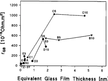
The calculated equivalent thickness of intergranular glass films is given in Table IV. Figure 13 shows the dependence of the normalized resistivity at 673 K ver-sus the equivalent film thickness. The threshold for the constant resistivity is found at 1-2 nm. This equilibrium film thickness value corresponds to two to four mono-layers of SiO4-tetrahedra of the dimension of 0.48 nm.
The macroscopic grain boundary resistivities at 673 K as a function of the annealing time at 1773 K are shown in Fig. 14. During the annealing process the macroscopic specific grain boundary resistivities decrease in samples B-10 and C-10, in which the equilibrium thickness of intergranular glass films has already been achieved. On the other hand, in samples having low glass contents (R-0, A-7, C-l, and E-10), the value of the macroscopic grain boundary resistivity remains constant. This behavior can be assigned to the grain coarsening which reduces the number of the grain
M. Godickemeier ef al.: Effect of intergranular glass films on the electrical conductivity of 3Y-TZP E
o
9 o m (9 1200 1000 800 600 4 0 0 200 -1 2 3 4 5 6Equivalent Glass Film Thickness [nm]
FIG. 13. Normalized grain boundary resistivity at 673 K as a function of the equivalent thickness of the intergranular film.
boundaries perpendicular to the current direction. Only in "saturated" samples the glass phase is squeezed out from the grain boundaries during the grain growth.
D. Specific properties and the equilibrium film thickness
The microscopic specific electrical properties of the intergranular phase, crGB (eq) and eGB (eq), shown in
Table IV, were derived according to Eqs. (1) and (2) from the calculated values of equivalent thickness <5GB
(eq) and the experimentally found macroscopic values of PGB and CQB (Table III). The resulting microscopic spe-cific conductivity of the intergranular phase at 673 K varies between 1.1 X KT6 S/m and 1.6 X 10"5 S/m
and the dielectric constant from 0.5 to 130.8 at 693 K. However, at low glass phase contents the estimated equivalent mean thickness is smaller than the expected
2000 E O m (3 1500 1000 500
-Time [h]
FIG. 14. Macroscopic specific grain boundary resistivity at 673 K as a function of annealing time.
equilibrium value of 1—2 nm, and a continuous inter-granular glass layer cannot be formed. As a result, the current path partially avoids crossing the disjointed glass films and shunt over the "clean" grain boundaries. This parallel current path results in lower values of PGB (Table III) and crGB (eq), as well as in too low values
of eGB (eq) for the samples TZ-3Y, R-0, C-l, and the whole A and E series. On the other hand, for equiva-lent thicknesses much exceeding the equilibrium width of intergranular films (samples B-10, C-10, and F-46), too high values for crGB (eq) and eGB (eq) are obtained.
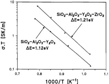
In order to verify these results, we want to compare the specific properties of the glass phase which we found by analyzing the experimental results using the brick layer model with the properties of bulk glass material. Two glasses have been prepared by melting the appropriate amounts of oxides at 1973 K. The first glass with the eutectic composition of the SiO2-Al2O3-Y2O3
system (46 wt. % SiO2, 22 wt. % A12O3, and 32 wt. %
Y2O3) melts at 1617 K.44"46 The second glass that was
prepared as a bulk sample corresponds to the quater-nary composition found in the three grain junctions by EDX analysis (42 wt. % SiO2, 22 wt. % A12O3, 21 wt. %
Y2O3, and 15 wt. % ZrO2).
Figure 15 shows the temperature dependences of the permittivity, e', and Fig. 16 the Arrhenius plots of the conductivities of both glasses. At 693 K the permittivity of the ternary eutectic glass is 7.5 and that of the quaternary glass containing ZrO2 is 15.7.
The corresponding specific conductivities at 693 K are 5.18 • 10"7 S/m for the ternary glass and 6.34 • 10"7 for
the quaternary one. The activation energies of the elec-trical conductivities of these glasses are 1.11 ± 0.02 eV and 1.21 ± 0.02 eV, respectively. All these properties are in good agreement with the values of the specific properties of the intergranular glass phase, calculated
500 600 700 600 900 1000 1100 1200
Temperature [K]
FIG. 15. The temperature dependence of the real part of the complex dielectric permittivity of SiO2-Al2O3-Y2O3-(ZrO2) glasses (for compositions, see text).
M. Godickemeier et al.: Effect of intergranular glass films on the electrical conductivity of 3Y-TZP
1000
0.1
-11
1000/T [K
FIG. 16. Arrhenius plots of the electrical conductivities of SiC>2-glasses (for compositions, see text).
from the polycrystalline ceramic samples according to the "brick-layer" model (see Tables IV and V).
E. The characteristic temperature Tb
Typical temperature dependences of both the intra-grain and intra-grain boundary conductivity of 3Y-TZP, as de-termined from ac-impedance spectroscopy for the sample E l , are shown as Arrhenius plots (log a'T against \/T) in Fig. 17. The slopes of the Arrhenius plots reveal the corresponding activation energies of
a'. It can be seen that the ionic conductivity of the
bulk material (grains), which is almost the same for all samples, has a lower activation energy than the conduc-tivity of the grain boundaries. Consequently, the two
TABLE V. Activation energies, the characteristic temperature 7 j , and the equilibrium thickness of intergranular glass films.
Sample TZ-3Y R-0 A-3 A-5 A-7 B-3 B-5 B-10 C-l C-5 C-10 D-3 D-5 D-10 E-3 E-5 E-10 F-46 A £G (eV) 0.94 0.93 0.93 0.93 0.91 0.94 0.92 0.93 0.93 0.92 0.92 0.93 0.90 0.92 0.93 0.93 0.92 0.93 A * G B (eV) 1.18 1.12 1.13 1.10 1.12 1.14 1.10 1.13 1.15 1.12 1.12 1.11 1.15 1.10 1.12 1.12 1.12 1.15 r»(K) 615 650 1030 1130 920 1360 3760 2040 890 3520 3350 770 1760 1430 1060 780 810 2800 S G B (nm) 1.26 0.84 0.75 1.17 0.92 1.44 1.11 1.24 1.19 1.11 1.30 1.19 1.17 1.65 1.32 1.09 1.15 1.95 0.01 1 1.1 1.2 1.3 1.4 1.5 1.6 1.7 1.8 1000/T [1/K]
FIG. 17. Arrhenius plots of grain and intergrain conductivities (sam-ple E-l).
Arrhenius lines for the grains and grain boundaries intersect at high temperatures.
The temperature at the point of intersection, Tb, which increases with increasing grain boundary film thickness, is the characteristic temperature of the inter-granular conductivity blocking, which is caused by the intergranular glass phase films. At temperatures lower than Tb, the macroscopic specific grain boundary re-sistivity, P'GB, exceeds the specific resistivity of the grains, pG. The total (dc) specific resistivity, p'T, is then determined by the predominating resistivity of grain boundaries (p'T = PGB)- At temperatures higher than Tb, the macroscopic grain boundary resistivity, pGB, becomes negligibly small in comparison to the resistivity of grains, and the total specific resistivity, p'T, reveals the properties of the bulk material (p'T = p'G).
A change in the slope of Arrhenius plots of total con-ductivity is observed at the characteristic blocking tem-perature Tb, at which the low-temperature grain boundary controlled conduction turns into a high-temperature re-gion of lattice-diffusion determined charge transport. At this temperature the macroscopic resistivity of grain boundaries is equal to the macroscopic resistivity of grains, both of which are exactly one-half of the total sample resistivity (p'GB = PG = l/2pr)- T m s behavior
is schematically shown in Fig. 18.
The characteristic temperatures, Tb, of the 3Y-TZP samples (Table V) were determined as the intercept points of the Arrhenius lines of the grain boundary and grain conductivities and are plotted in Fig. 19 ver-sus the equivalent thickness of the glass phase §GB
(eq). A constant saturation value is found if the cal-culated equivalent thickness of the intergranular film exceeds about 1-2 nm, similar to the results shown in Fig. 13.
The characteristic temperatures, Tb, and the ac-tivation energies of the conductivity both within the
M. Godickemeier et al.: Effect of intergranular glass films on the electrical conductivity of 3Y-TZP CO aa.T"CTa B.T Parallel resistors: aT.T=aa.T+aaB.T 1.5 1.1 1.2 1.3 1.4
1000 / T [K"
1]
FIG. 18. The transition from the grain boundary to the grain conduc-tivity controlled region (schematically).
grains and in the grain boundaries are given in Table V, together with the equilibrium thickness of intergranular films, SGB, calculated according to Eq. (2) from the macroscopic grain boundary capacitance CGB (Table III), using the known permittivity of the glass phase of 15.7 at 693 K (see Fig. 15). It can be seen that even the TZ-3Y sample with the least amount of glass shows a Tb of 615 K. The activation energy of the conductivity of the bulk grain material, A£G, is 0.92-0.93 ± 0.02 eV for
all samples. The activation energy of the conductivity of grain boundaries, A.ZJGB, was found to vary from 1.10 ± 0.02 to 1.18 ± 0.02 eV.
IV. CONCLUSIONS
A change in the slope of the Arrhenius plots of total conductivity toward lower activation energy occurring in 3Y-TZP at a characteristic temperature T\, is caused
4000 3000 2000 1000 - TZ0 -A^E3 3f R0 *3 C5 ' D5 f D1O B3 T B5 CIO • F50-> B10 0 1 2 3 4 5 6
Equivalent Glass Film Thickness [nm] FIG. 19. The dependence of the characteristic grain boundary block-ing temperature Tf, on the calculated equivalent thickness of inter-granular films.
by an additional resistance of intergranular glass films in series with the bulk material. The thickness of these glass films is limited by a maximum equilibrium value of 1-2 nm. Our results show that the "brick-layer" concept allows one to evaluate the equivalent thickness of intergranular films and even the specific properties of the glass phase.
In order to describe the complex total conductivity behavior of solid ceramic electrolytes, the combined in-fluence of the lattice and microstructural defects, such as dopant atoms, dislocations, grain boundaries, phase seg-regations, pores and microcracks, which may be present both in series and parallel connections, should be taken into account. The behavior between the stage II and stage III can be modeled by an equivalent electrical
cir-cuit of two resistors in series: pT = p'c + PGB- At low temperatures the macroscopic resistivity of grain bound-aries is higher than that of the bulk material, and the charge transport in 3Y-TZP ceramics is suppressed. Due to the higher activation energy, the macroscopic spe-cific resistivity of the grain boundaries decreases with increasing temperature faster than that of the bulk. At the characteristic temperature Tb, the resistivity values of grains and grain boundaries become equal. Above this temperature the resistivity of grain boundaries is negli-gible and the resistivity of grains determines the total resistivity of the ceramics. On the other hand, if the
par-allel electrical circuit of two resistors would be used, for
which the total conductivity is the sum of both conduc-tivity values, the bend in Arrhenius plot would have to occur from the lower to the higher activation energy with increasing temperature. Such behavior is known to exist between the intrinsic stage I and the extrinsic stage II:
aT = a'j + cr'E. However, this high-temperature bend of Arrhenius plots has not yet been observed in doped zirconias, since an appreciable concentration of intrinsic defects is formed only above 2000 K.55
ACKNOWLEDGMENTS
This work was financially supported by the Alusuisse-Lonza Corporation and the Swiss Federal Office of Energy (OFEN). The authors express their gratitude to Dr. L. Dubai from OFEN for his support and continuous interest and Professor P.D. Ownby for helpful discussions and reviewing the manuscript.
REFERENCES
1. A.J.A. Winnubst, P.J.M. Kroot, and A.J. Burggraaf, J. Phys. Chem. Solids 44, 955 (1983).
2. A.J.A. Winnubst, M.J. Verkerk, and A.J. Burggraaf, in Ad-vances in Ceramics: Vol. 7, edited by M. F. Yan and A. H. Heuer (American Ceramic Society, Inc., Westerville, OH, 1983), p. 177. 3. H. Schubert, N. Clausen, and M. Riihle, in Advances in
Ceram-ics: Vol. 12, edited by N. Clausen, M. Riihle, and A. H. Heuer (American Ceramics Society, Inc., Westerville, OH, 1984), p. 766.
M. Godickemeier et al.: Effect of intergranular glass films on the electrical conductivity of 3Y-TZP
4. A.J. Burggraaf, M. Van Hemert, D. Scholten, and A.J. A. Winnubst, Mater. Sci. Monogr. 28B, 797 (1985).
5. R. Chaim, D. G. Brandon, and A. H. Heuer, Acta Metall. 34, 1933 (1986).
6. R. K. Slotwinski, N. Bonanos, and E.P. Butler, J. Mater. Sci. Lett. 4, 641 (1985).
7. M.L. Mecartney, J. Am. Ceram. Soc. 70, 54 (1987).
8. M. J. Verkerk, A. J. A. Winnubst, and A. J. Burggraaf, J. Mater. Sci. 17, 3113 (1982).
9. M. J. Verkerk, B. J. Middelhuis, and A. J. Burggraaf, Solid State Ionics 6, 159 (1982).
10. M. Miyayama, H. Yanagida, and A. Asada, Am. Ceram. Soc. Bull. 64, 660 (1985).
11. S.P. S. Badwal and A.E. Hughes, in Proc. 2nd Int. Symp. Solid Oxide Fuel Cells, edited by F. Grosz, P. Zegers, S. C. Singhal, and O. Yamamoto (Commission of European Communities Rep. EUR 13546 EN, Luxembourg, Belgium, 1991), p. 445.
12. D.R. Clarke, in Mat. Sci. Res. Vol. 21, edited by J.A. Pask and A. G. Evans (Plenum Press, New York and London, 1987), p. 569. 13. D. R. Clarke, J. Am. Ceram. Soc. 70, 15 (1987).
14. S.P.S. Badwal and J. Drennan, J. Mater. Sci. 22, 3231 (1987). 15. R. Raj, J. Am. Ceram. Soc. 64, 245 (1981).
16. T. Stato, M. Nauer, and C. Carry, J. Am. Ceram. Soc. 74, 2615 (1991).
17. E. P. Butler and J. Drennan, J. Am. Ceram. Soc. 65, 474 (1982). 18. J. Drennan, M.V. Swain, and S.P.S. Badwal, J. Am. Ceram.
Soc. 72, 1279 (1989).
19. S.P.S. Badwal, F.T. Ciacchi, M.V. Swain, and V. Zelizko, J. Am. Ceram. Soc. 73, 2505 (1990).
20. M. J. Verkerk (Ph.D. Thesis, University of Twente, The Nether-lands (1982).
21. S.P.S. Badwal, J. Mater. Sci. 19, 1767 (1984). 22. S. P. S. Badwal, J. Am. Ceram. Soc. 73, 3718 (1990).
23. D. K. Hohnke, in Fast Ion Transport in Solids, edited by P. Vaskista, J. N. Mundy, and G. K. Shenoy (Elsevier North-Holland, Inc., New York, 1979), p. 669.
24. A. Nakamura and J. B. Wagner, J. Electrochem. Soc. 133, 1542 (1986).
25. M. Weller and H. Schubert, J. Am. Ceram. Soc. 69, 573 (1986). 26. M. Weller and H. Schubert, in Solid State Ionics, edited by M. Balkanski, T. Takahaski, and H.L. Tuller (Elsevier Science Publishers B. V., Amsterdam, The Netherlands, 1992), p. 569. 27. A. S. Nowick and D. S. Park, in Superionic Conductors, edited by
G. Mahan and W. Roth (Plenum Press, New York, 1976), p. 395. 28. S.P.S. Badwal, J. Mater. Sci. 18, 3117 (1983).
29. A. Orliukas, B. Heeb, B. Michel, K. Sasaki, P. Bohac, and L. Gauckler, in Proceedings Europ. Ceram. Soc. 2nd Conference, Augsburg, Germany, Sept. 11-14, 1991 (to be published). 30. H. Ohno, T. Nagasaki, T. Ishiyama, Y. Katano, and H. Katsuta,
J. Nucl. Mater. 141-143, 392 (1986).
31. A. S. Nowick, D. Y. Wang, D. S. Park, and J. Griffith, in Fast Ion Transport in Solids, edited by P. Vashista, J. N. Mundy, and G. K. Shenoy (Elsevier North-Holland, Inc., New York, 1979), p. 673. 32. F. K. Moghadam, T. Yamashita, and D. A. Stevenson, in Advances
in Ceramics: Vol. 3, edited by A. H. Heuer and L. W. Hobbs (American Ceramics Society, Inc., Westerville, OH, 1981), p. 364. 33. C. Pascual, J.R. Jurado, and P. Duran, J. Mater. Sci. 18, 1315
(1983).
34. F. Moztarzadah, Ceram. Int. 14, 27 (1988).
35. E. C. Subbarao and T. V. Ramakrisnan, in Fast Ion Transport in Solids, edited by P. Vashista, J. N. Mundy, and G. K. Shenoy (Elsevier North-Holland, Inc., New York, 1979), p. 653. 36. N. Bonanos, R.K. Slotwinski, B.H. Steele, and E.P. Butler,
J. Mater. Sci. Lett. 3, 245 (1984).
37. M. Kleitz, H. Bernard, E. Fernandez, and E. Schouler, in Advances in Ceramics: Vol. 3, edited by A. H. Heuer and L. W. Hobbs (American Ceramics Society, Inc., Westerville, OH, 1981), p. 310. 38. C. G. Koops, Phys. Rev. 83, 121 (1951).
39. J. E. Bauerle, J. Phys. Chem. Solids 30, 2657 (1969).
40. A. Orliukas, K. Sasaki, P. Bohac, and L. Gauckler, in Proc. 2nd Int. Symp. Solid Oxide Fuel Cells, edited by F. Grosz, P. Zegers, 5. C. Singhal, and O. Yamamoto (Commission of European Com-munities Rep. EUR 13546 EN, Luxembourg, Belgium, 1991), p. 377.
41. R.E.W. Casselton, Phys. Status Solidi A 2, 571 (1970). 42. P. V. Ananthapadmanabhan, N. Venkatramani, V. K. Rohagi,
A. C. Momin, and K. S. Venkateswarlu, J. European Ceram. Soc. 6, 111 (1990).
43. J. F. Baumard, P. Papet, and P. Abelard, in Advances in Ceramics: Vol. 24, edited by S. Somiya, N. Yamamoto, and H. Yanagida (American Ceramics Society, Inc., Westerville, OH, 1988), p. 779.
44. S. P. S. Badwal and A. E. Hughes, J. European Ceram. Soc. 10, 115 (1992).
45. M. Kleitz and J. H. Kennedy, in Fast Ion Transport in Solids, edited by P. Vashista, J. N. Mundy, and G. K. Shenoy (Elsevier North-Holland, Inc., New York, 1979), p. 185.
46. L. Dessemond, J. Guindet, A. Hammou, and M. Kleitz, in Proc. 2nd Int. Symp. Solid Oxide Fuel Cells, edited by F. Grosz, P. Zegers, S. C. Singhal, and O. Yamamoto (Commission of Euro-pean Communities Rep. EUR 13546 EN, Luxembourg, Belgium, 1991), p. 409.
47. H. E. Exner and H. P. Hougardy, Einfiihrung in die Quantitative Gefiigeanalyse (DGM Informationsgessellschaft Verlag, 1986), p. 30.
48. E. E. Underwood, A. R. Colcord, and R. C. Waugh, in Proc. 3rd Int. Mater. Symposium, edited by R.M. Fulrath and J.A. Pask (John Wiley and Sons, Inc., New York, 1968), p. 25.
49. T. van Dijk and A. J. Burggraaf, Phys. Status Solidi A 63, 229 (1981).
50. B.C.H. Steele, J. Drennan, R.K. Slotwinski, N. Bonanos, and E. P. Butler, in Advances in Ceramics: Vol. 3, edited by A. H. Heuer and L. W. Hobbs (American Ceramics Society, Inc., West-erville, OH, 1981), p. 286.
51. S. Rajendran, J. Drennan, and S.P.S. Badwal, J. Mater. Sci. Lett. 6, 1431 (1987).
52. LA. Bondar and F.Y. Galakhov, Izv. Akad. Nauk. SSSR, Ser. Khim, 7, 1231 (1964).
53. E. M. Levin, C. R. Robbins, and H. F. McMurdie, Phase Diagrams for Ceramists (Supplement, Am. Ceram. Soc, Inc., Westerville, OH, 1969), Fig. 2586.
54. M. J. Hyatt and D. E. Day, J. Am. Ceram. Soc. 70, C283 (1987). 55. P. Aldebert and J. P. Traverse, J. Am. Ceram. Soc. 68, 34 (1985).