HAL Id: hal-01898582
https://hal.archives-ouvertes.fr/hal-01898582
Submitted on 18 Oct 2018
HAL is a multi-disciplinary open access
archive for the deposit and dissemination of
sci-entific research documents, whether they are
pub-lished or not. The documents may come from
teaching and research institutions in France or
abroad, or from public or private research centers.
L’archive ouverte pluridisciplinaire HAL, est
destinée au dépôt et à la diffusion de documents
scientifiques de niveau recherche, publiés ou non,
émanant des établissements d’enseignement et de
recherche français ou étrangers, des laboratoires
publics ou privés.
An optimization formulation of converter control and its
general solution for the four-leg two-level inverter
Abdelkader Bouarfa, Marc Bodson, Maurice Fadel
To cite this version:
Abdelkader Bouarfa, Marc Bodson, Maurice Fadel. An optimization formulation of converter
con-trol and its general solution for the four-leg two-level inverter. IEEE Transactions on Concon-trol
Sys-tems Technology, Institute of Electrical and Electronics Engineers, 2018, 26 (5), pp.1901 - 1908.
�10.1109/TCST.2017.2738608�. �hal-01898582�
Abstract—The paper proposes an optimization formulation of the control problem for power electronic converters. A benefit of the approach is a systematic method for the control of high switch-count static converters. In the case of the 3-phase, 4-leg, 2-level inverter, the framework provides a characterization of all the possible solutions that yield a maximal extension of the invert-er linearity range. The method makes it possible to recovinvert-er well-known modulation strategies, as well as to discover some new ones having different properties and distinct advantages. The characteristics resulting from different design choices are evalu-ated in simulations, with consideration being given to the linearity range, total harmonic distortion, and switching losses. Key prin-ciples of extension of the proposed method to multilevel, multileg converters are given, as well as motivations for an FPGA-based hardware implementation enabling real-time PWM control.
Index Terms—Voltage source inverter, 4-leg 2-level inverter, voltage control, PWM, control allocation, optimization, simplex algorithm, median voltage injection.
I. INTRODUCTION
IXED high switching-frequency pulse-width modulation (PWM) is an essential class of modulation methods for power converters [1], [2]. For the widely-studied 3-leg 2-level inverter, two popular PWM methods are: (1) carrier-based
pulse-width modulation (CBPWM) [1]–[3], using
low-frequency modulating signals and a high-low-frequency carrier wave, and (2) space vector theory, using a 3-phase geometric vector representation of the inverter and leading to the well-established space vector modulation (SVM) techniques [1], [2], [4], [5]. The main theoretical differences between CBPWM and space vector theory are related to the way the degree of freedom left in the inverter is exploited [1], [6]–[12]. Typically, this degree of freedom is used to increase the in-verter linearity range [4]–[7], [13], [14], to reduce switching losses [15], [16], or to mitigate current harmonics using subop-timal modulating solutions [17]–[18].
However, the difficulty of developing control strategies
in-A. Bouarfa (corresponding author) and M. Fadel are with LAPLACE, Université de Toulouse, CNRS, INPT, UPS, France: 2 rue Charles Camichel, F-31071 Toulouse, France (bouarfa@laplace.univ-tlse.fr, fadel@laplace.univ-tlse.fr).
M. Bodson is with University of Utah, Dept. Electrical and Computer En-gineering, 50 S Central Campus DR RM 2110, Salt Lake City UT 84112-9206, USA (bodson@ece.utah.edu).
creases rapidly as the number of switches grows, especially with the widely-used space-vector representation.For the 4-leg 2-level inverter, the addition of the fourth-leg raises the num-ber of possible locations of a reference voltage vector from a 2D plane divided into 6 sectors [4], [5] to 24 tetrahedrons in a 3D representation [12], [19]–[21].
Starting from these observations, the paper proposes a new control strategy different from traditional PWM control and based on on-line numerical optimization using linear pro-gramming techniques. This strategy is expected to be more generic, to be less dependent on the switch count, and to avoid difficulties encountered with a geometric approach. The con-trol problem of the converter is formulated as an
under-determined constrained optimization problem. Such problem
is remarkably similar (although not identical) to the control
allocation problem studied previously in flight control and
marine applications [22], [23]. In this paper, the focus is placed on the 4-leg 2-level inverter, where a complete charac-terization of the solutions is possible without the use of numer-ical techniques, thus enabling a good understanding of the pos-sibilities opened by this new formulation.
A previous implementation of the control allocation ap-proach method for the 4-leg inverter was based on the descrip-tion of its active voltage vectors [24] and the regular-sampled symmetric PWM (RSPWM) [3]. The correct non-zero vector sequence was computed using a numerical optimization meth-od based on the simplex algorithm, removing the need to iden-tify a reference tetrahedron, as was done in earlier work.
Considering switching cells as available resources subjected to ranges of operation, a different control allocation method is introduced here, reducing the size of the problem considerably. Moreover, the paper proposes an analytical solution of the optimization problem that reduces the control of the inverter to the computation of the median of a special series. Furthermore,
CBPWM-equivalent formulas are given for modulation laws
derived from the new control allocation problem.
As constraints are taken into account in the optimization problem, solutions resulting from control allocation methods for power converters naturally yield a maximal extension of
the linearity range of the inverter [24], [25]. Specific choices
of the algorithm’s parameters produce modulation laws with different properties, all implementable with few computations. Under the general umbrella of the proposed strategy, not only
An optimization formulation of converter
con-trol and its general solution for the 4-leg 2-level
inverter
Abdelkader Bouarfa, Marc Bodson, Fellow, IEEE, and Maurice Fadel, Member, IEEE
are previously-proposed modulation laws found as special
cases, but new interesting modulation schemes are discovered
as well. Simulation results illustrate the properties of the dif-ferent methods obtained. Switching losses and total harmonic distortion (THD) on voltages and currents are evaluated in computations for comparison.
II. 4-LEG 2-LEVEL INVERTER ASSUMPTIONS FOR PWM CONTROL
A. Inverter and load
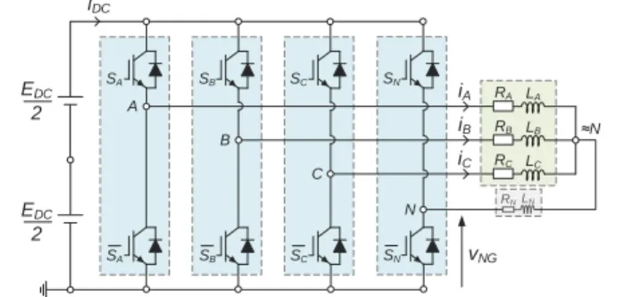
The 4-leg 2-level inverter is a well-proven solution for 3-phase systems with neutral wire, for applications like distribut-ed generation, active power filtering, common-mode active filtering or fault-tolerant operation of electric drives [12], [19]–[21]. Fig. 1 illustrates the inverter, star-connected to a load with per-phase resistances and inductances values RK, LK,
K{A,B,C,N}. The load can be unbalanced or nonlinear. The
fourth-leg (N) is connected to the neutral point of the load in order to control the neutral voltage and also handle possible unbalanced currents. Here, RN and LN are neglected, and the
ground reference G is the lower DC bus in order to facilitate the derivation of control equations. EDC is the DC bus voltage.
B. Switching cells
A switching cell is taken to be an association of two func-tional switches working at complementary binary states. Dead
times are neglected. Each leg is comprised of one switching
cell. For K{A,B,C,N}, the state of the switching cell K is the state of the corresponding upper switch, SK, equal to 0 when
the switch is off and 1 when the switch is on.
C. Output voltages, load voltages
The 4 output voltages VKG are referred to the ground G.
Re-garding the star-connection, it is useful to define for each of the three first legs a relative switching state SKN = SK − SN.
Then, the 3 independent load voltages, referred to the neutral point N, are given by VKN = EDC SKN, for K{A,B,C}.
D. Pulse-width modulation
The mean value DK =<SK>Ts of SK over the switching period
TS defines the duty cycle of the switching cell K, DK[0,1].
Mean-value references voltages are obtained with RSPWM by determining the gating pulses SK from the duty cycles DK as
illustrated on Fig. 2. The load voltage mean values are
AB C
VKN T EDC
DK DN
EDCDKN K S , , , The linearity range of the converter is defined here as the range of amplitude of the 3-phase sinusoidal reference voltage system for which the converter delivers a voltage system with the desired values. Because of the star-connection, with classic sinusoidal PWM (SPWM), the linearity range is restricted to
EDC/2. A common modification extends this range by varying
the neutral potential of the load. When the desired voltages are balanced and three-phase, the maximal output amplitude achievable linearly is 1/3·EDC, as for SVM [4], [5] or SPWM
with 1/6 third-harmonic injection (THIPWM1/6) [13], [14]. III. CONTROL ALLOCATION FOR INVERTER CONTROL
A. Control allocation methods
Control allocation methods were developed in aerospace problems as a solution for over-actuated systems subjected to
constraints [22], [23]. It is assumed that the process to be
con-trolled can be modeled by a constrained system of m control equations with n unknowns, with m<n:
Bua, umin uumax
The matrix B, of size m×n, specifies the effectiveness of the actuators. B is assumed to be of rank m (rows are linearly in-dependent). The vector u, of length n (column), is the control
vector that specifies the chosen use of actuators. The vector a,
of length m (column), is the resulting output vector. Denote
umin and umax (vectors) as the minimum and maximum bounds
of each component of the control vector u, respectively. One wants to find a control vector u to obtain a given desired out-put vector ad. Considering the constraints, the problem (2) may
have zero, one, or an infinity of solutions. Methods have been developed to extract a solution from the whole set of feasible solutions by formulating an optimization problem.
The objective of the 4-leg 2-level inverter control is to ob-tain a desired reference vector ad = Vref = (VANref, VBNref, VCNref)T
of 3 load voltages on average over the switching period TS. In
order to scale the voltages with respect to EDC, define the
scaled reference vector as ΔDref = Vref / EDC = (DANref, DBNref,
DCNref)T. Here, ΔDref is similar to the difference of duty cycles
between the three first legs and the fourth one, see (1). Then, the system of equations of (2) depends on the chosen control variables and the converter control requirements.
B. Switching cell formulation
The control problem can be formulated as finding duty cycle
SC SC SB SB EDC iDC 2 G EDC 2 SA SA LC N RC iC LB RB LA RA iB iA A B C vNG SN SN N RNLN
Fig. 1. Illustration of the 4-leg 2-level inverter connected to a three-phase load with impedances ZA, ZB, ZC.
DA t t SA Triangular carrier TS TS /2 DATS DATS 0 1 1 0
Fig. 2. Illustration of the realization of gating pulse on switch A of width
commands DS to the cells such that Dref MSDS, 0DS 1 1 1 0 0 1 0 1 0 1 0 0 1 S M D S
DA DB DC DN
T The switching cell formulation (3) is a simpler alternative to the space vector formulation in [24], introducing less control variables and a smaller matrix. In order to find a control solu-tion to the under-determined constrained control problem (3), the following optimization problem is defined:
1 0 subject to , min 1 0 S pref S S ref S S D D D D D D M J J S
The primary criterion Jctrl(DS) = ||MSDS − ΔDref||1 is a control error based on the control equation in (3). Because the
solu-tion is often not unique, the secondary criterion Jpref(DS) =
ε·|DS − DSpref| is a deviation error added to specify preferred
uses of the switches, where | | denotes the application of the element-wise absolute value. The column vector DSpref =
(DApref, DBpref, DCpref, DNpref)T corresponds to the preferred duty
cycle values. The row vector ε = (εA, εB, εC, εN) helps to give
further preference to one or more switches, which makes it possible to affect the weight of deviation errors from preferred positions in Jpref. Although the parameters εK can be real
num-bers, we will restrict them to be integers, with little loss of generality. This choice will result in a simple solution of the optimization problem. Finally, the small real parameter ε0
gives priority to the minimization of the control error Jctrl [22].
The optimal solutions are determined by the choice of the parameters DSpref and ε, which produce a large number of
pos-sible configurations. We will discuss a few choices in the next sections. The associated control diagram is shown on Fig. 3.
IV. CHARACTERIZATION OF ALL FEASIBLE SOLUTIONS WHEN THE REFERENCE IS ACHIEVABLE
A. Constraint set when the reference is achievable
When the reference vector is achievable, the optimization problem can be simplified. Solutions can be determined ana-lytically, depending on the parameters DSpref, and ε. This leads
to relatively simple expressions of the modulating signals. Due to the particular form of MS, the solutions that achieve
the reference can be characterized by the single variable DN:
N ref KN K D D D C B A K , , , If there is at least one positive and one negative voltage in the reference vector (it is the case if the reference voltage vector is three-phase), bounds DNmin and DNmax can be defined as
ref N
ref
N D D D
D min min , max 1max
and the whole set of feasible solutions that achieve the refer-ence vector is described by constraints on DN alone:
DN
DNmin,DNmax
,Jctrl
DN 0 Therefore, as long as the constraint set is not empty, i.e., as long as DNmin ≤ DNmax, any signal resulting from solutions of
(5) will achieve a maximal linearity range.
B. Reduction of the solution to a single decision variable
The secondary criterion to be minimized is ABCN K Kpref K K S pref D D D J
, , , ) (
By defining a series dmod of elements dmodK as
ref KN pref K K D D d C B A K , , , mod
N C B A K K pref N N D d ddmod mod mod , , ,
and by substitution in (25), the criterion Jpref can be now
re-formulated as an explicit function of DN:
ABCN N K K K N pref D D d J mod , , , ) (
that is a sum of distances on the real-axis from DN to the points
dmodK and weighted by the parameters εK. The single decision
variable DN solely represents the available functional degree of
freedom. The optimization problem is considerably simplified.
C. Solution of the optimization problem
The minimization of sums of weighted absolute deviations from a unique number (here DN) to other fixed numbers (here
dmodK) is a well-known mathematical problem [26]–[30]. Here,
the solution is introduced thanks to the definition of the special series dmodε, for which each dmodK appears εK times.From [26]–
[30], it can be deduced that, without considering constraints, the solution of the minimization of (13) reduces to the
deter-mination of the median (denoted med) of the series dmodε for
all values of the design parameters.
The sum of all the εK gives the size (or number of elements)
of dmodε. In practice, two distinct cases are encountered: (1) the
series dmodε is of odd size: the optimal value of DN denoted
DNopt is the midpoint of the series and is unique; (2) the series
dmodε is of even size: DNopt is a set of values of DN belonging to
the segment delimited by the two midpoints of the series. Fig. 4 illustrates the optimal solutions depending on the na-ture of the size of dmodε. The criterion Jpref is a piecewise linear
function due to the use of absolute values. The “even” case in Fig. 4 (a) is inconvenient because there is an infinite number of solutions, and control is not uniquely determined. In practice, a
Iref ε DS Load VANref VBNref VCNref 3 3 4 CURRENT LOOP (OPTIONAL) 4 S Imeas 3 VAN VBN VCN 3 VOLTAGE REFS DSpref PARAMETERS DUTY CYCLES OUTPUT VOLTAGES SWITCHING STATES 4-leg 2-level inverter
Current Reg. CONTROL PART PHYSICAL PART Control Allocation + -0 1 0 TRIANGULAR CARRIER RELAY MODULATOR DS S
slight adjustment of the problem statement is sufficient to make the optimal solution unique, as shown in Fig. 4 (b).
Finally, the median set of the series dmodε has to be con-strained by the bounds DNmin and DNmax in order to obtain
fea-sible solutions. Therefore, optimal solutions ofthe constrained problemare the elements DNopt belonging to the intersection of
the median set of dmodε and of the segment [DNmin, DNmax].
D. Special choices of parameters
The choice of parameters DSpref and ε has a direct and
signif-icant effect on the nature of dmodε, on the optimal set of DN, and
on the resulting modulation strategy. Sets of parameters having interesting practical implications are given as examples.
The adjustment of DSpref translates into preferred duty cycle
values of for each switch. The most common choices for DSpref
would be DSpref {(0…0)T, (1…1)T, (0.5…0.5)T}.
The first obvious choice of ε is a vector of ones, implying no discrimination between switches. More generally, to avoid non-symmetric behavior with respect to the three phases, the
first three weights should be identical. This yields the
follow-ing propositions for adjustfollow-ing ε: {(1…1), (1 1 1 0), (0 0 0 1)}. V. EXAMPLES & SIMULATION RESULTS
Specific solutions are derived and illustrated for the most in-teresting choices of parameters DSpref and ε, as summarized in
Table I. Simulations are carried out in the MATLAB Simulink environment. Evaluations of switching losses, THD on voltag-es and THD on currents are given later for comparison.
For the following figures showing duty cycles, the scaled reference amplitude value increases from left (a) to right (c) until the limit of 1/3 is reached. A whole fundamental period is illustrated. Reference voltages are chosen to be three-phase
and balanced for simplicity, but the method also works with
unbalanced references. As it will be useful for determining optimal solutions, we denote ΔDmed = med ΔDref the median of
the scaled reference vector.
A. Configuration 1
Selected configuration: First of all, consider the natural
choice where all preferred duty cycles are set to 0.5, which
means DSpref = (0.5 0.5 0.5 0.5)T and ε = (1 1 1 1).
Determination of the median: As all the εK are identical, all
the dmodK have the same occurrence in the series dmodε:
0.5 ,0.5 ,0.5 ,0.5
mod DANref DBNref DCNrefd
The size is even. Therefore, optimal solutions DNopt belong to
the segment defined by the two midpoints of dmodε. In the case
where the reference system is three-phase, 0.5 is necessarily one of the two midpoints of dmodε. The second midpoint is
linked to ΔDmed. Consequently,
meddmod
0.5Dmed,0.5
Remark: If ΔDmed is negative, the segment [0.5−ΔDmed, 0.5]
has to be replaced by [0.5, 0.5−ΔDmed]. For simplicity, this trivial adjustment will be assumed to be made if necessary.
Optimal solutions: Finally, optimal solutions are any value
belonging to [0.5−ΔDmed, 0.5] and saturated by [DNmin, DNmax].
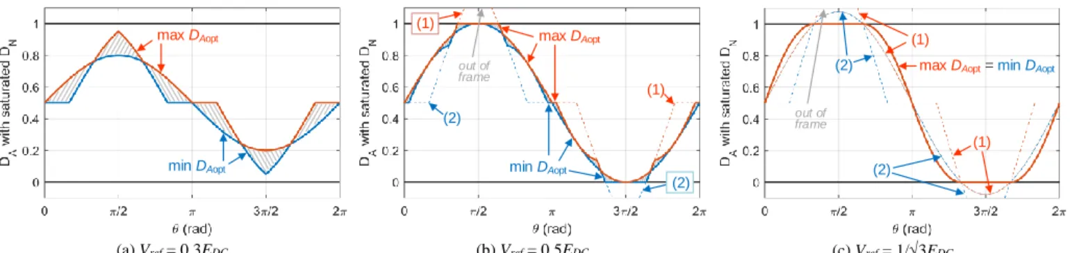
Fig. 5 gives an illustration of the domain of the DNopt
wave-forms. The bounds DNmin and DNmax are represented by the
ex-tremal bold lines, delimiting the saturation domain. As the reference amplitude increases, the saturation domain becomes narrower. The scaled value of 1/3 is the limit where for some instants =k/3, k{0,...,6}, the two extremal bold lines meet, meaning that DNmin is equal to DNmax, see Fig. 5 (c).
In Fig. 5, the two plain midlines draw the bounds of the op-timal domain of DN (hatched area). As the scaled amplitude
increases, the median segment grows wider and eventually encounters the saturation domain (from (b)). The two lines labelled (1) and (2) correspond to the maximum and minimum bounds of the nonsaturated optimal solution set, respectively.
Fig. 6 shows the optimal domain of the DA waveforms,
de-termined from the optimal domain of DN by using (6). The
fundamental wave is represented by the dashed gray midline (when visible). As for Fig. 5, the optimal domain of DA
ob-tained if DN’s is not saturated is represented by the lines
la-belled (1) and (2). The parts of any optimal saturated DN
mod-ulating signal that encounters the bounds DNmin or DNmax
corre-spond to periods where a leg is continuously clamped to the DC bus or to the ground, as observed on Fig. 6 (b)–(c).
When DN is not saturated, a certain regular waveform of DA
is identified, which stays proportional to the reference ampli-tude until saturation appears. Then, as a result of the satura-tion, the optimal domain of DA changes form compared to
Fig. 6 (a) in order to achieve the correct fundamental wave. This particular property is shared by most of modulation strat-egies obtained from the proposed control allocation method.
DN
dmod B
0 0.5 1
dmod C dmod N dmod A
Jpref
DN
dmod B dmod C dmod N dmod A
0 1
Jpref,opt
med dmodε
DIS TRIBUTIO N OF ARBITRARY dmod
GENERAL TREND OF Jpref WITH ε=(1111)
DNopt
DNmin DNmax
+ _
DN
dmod B dmod C dmod N dmod A
0 1
med dmodε
DNopt Jpref
Jpref,opt
GENERAL TREND OF Jpref WITH ε=(1211)
DN
+ _
Fig. 4. Illustration of the effect of parameters on the solving of the simpli-fied optimization problem with arbitrary ΔDref. DSpref = (0.5 0.5 0.5 0.5)T.
TABLEI
CONFIGURATION EXAMPLES OF THE CONTROL ALLOCATION METHOD
n° DSpref T ε Resulting PWM laws
1 (0.5 0.5 0.5 0.5) (1 1 1 1) undetermined 2 (0.5 0.5 0.5 0.5) (1 1 1 0) OMIPWM [25]
3 (0.5 0.5 0.5 0.5) (0 0 0 1) ASPWM
4 (1 1 1 1) (1 1 1 1) DPWMmax [1], [9], [11]
~ (0 0 0 0) (1 1 1 1) DPWMmin [1], [9], [11]
OMIPWM: opposite median-voltage injection PWM; ASPWM: adaptive sinus PWM; DPWM: discon-tinuous PWM.
B. Configuration 2
Selected configuration: With the previous configuration, the
optimal solution was not unique. In order to force the series to be of odd cardinal, a first possibility is to remove the prefer-ence on the fourth duty cycle that controls the neutral potential while keeping the symmetry between the three phases. This leads to DSpref = (0.5 0.5 0.5 0.5)T and ε = (1 1 1 0).
Determination of the median: dmodN does not appear in the
series dmodε and, as the other εK are identical,
DANref DBNref DCNref
dmod 0.5 ,0.5 ,0.5
Thus, the median is directly given by med dmodε = 0.5–ΔDmed. Optimal solution: the optimal value DNopt is unique and is
equal to 0.5–ΔDmed saturated by [DNmin, DNmax]. It corresponds
to parts of the optimal domain given by the previous configu-ration and farthest from 0.5 in Fig. 5. Thanks to the analytical solution, a carrier-based equivalent method can be given. It consists in injecting the opposite of the median reference in the waveform of DN as a zero-sequence signal. This new
mod-ulation method was recently proposed in [25] under the name of opposite median-voltage injection PWM (OMIPWM). Un-like SVM, where the zero-sequence signal always corresponds to the value of the midpoint between DNmin and DNmax (see [6],
[8]–[11], [16], [25]), DN will tend to reach the bounds DNmin
and DNmax for OMIPWM. From a certain reference amplitude
value, discontinuous modulation appears with increasing dis-continuous periods. This feature is highlighted in Fig. 5 (b)–(c) at =/6+k/3, k{0,…,5}. OMIPWM is a new method, easy to implement, which automatically ensures the transition from a continuous to a discontinuous modulation scheme as a func-tion of the reference amplitude [25].
C. Configuration 3
Selected configuration: another possibility is to place a
preference for the fourth duty cycle at 0.5, which means keep-ing the neutral potential nearest to half of the DC bus voltage:
DSpref = (0.5 0.5 0.5 0.5)T and ε = (0 0 0 1).
Determination of the median: This time, only εN is non-null.
dmodN = 0.5 is the only element of dmodε, thus, med dmodε = 0.5. Optimal solution: DNopt is unique and corresponds to the
value 0.5 saturated by [DNmin, DNmax].
Fig. 7 shows the resulting optimal waveform of DN. In fact,
most of the time, the optimal solution corresponds to SPWM, as shown on Fig. 8. However, SPWM has a linearity range limited to the scaled amplitude value of 0.5. As can be de-duced from Fig. 7 (b), the constant DN solution value of 0.5
starts to be saturated by the bounds DNmin and DNmax. It gives
the minimal adjustment of the neutral potential needed to achieve the reference. A benefit of the optimal solution given by configuration 3 is that, unlike for SPWM, the maximal limit of 1/3 is reached. It appears that this solution has not been proposed before in the literature. The associated modulation law is called here adaptive sinus PWM (ASPWM).
D. Configuration 4
Selected configuration: it is also possible to adjust DSpref in
order to specify a preferred value of duty cycle. For configura-tion 4, we set DSpref = (1 1 1 1)T and ε = (1 1 1 1).
Determination of the median: the median of the series
med dmodε is not reduced to a unique element. It corresponds to
[1–ΔDmed, 1] and it is always out of the saturation domain. Optimal solution: With the selected vector DSpref, the
opti-mal solution is DNmax, whatever the reference amplitude value
is (of course comprised between 0 and 1/3). This solution
DNmax DNmin max DNopt min DNopt DNmax DNmin min DNopt max DNopt (1) (2) DNmax DNmin (1) (2)
max DNopt=min DNopt
(a) Vref = 0.3EDC (b) Vref = 0.5EDC (c) Vref = 1/3EDC
Fig. 5. Optimal waveforms of DN with DSpref = (0.5 0.5 0.5 0.5)T, ε = (1 1 1 1). Labels (1) and (2) indicate nonsaturated lines for max, min DNopt, respectively. max DAopt min DAopt max DAopt min DAopt (1) out of frame (1) (2) (2)
max DAopt=min DAopt
(1) (2) out of frame (1) (2)
(a) Vref = 0.3EDC (b) Vref = 0.5EDC (c) Vref = 1/3EDC
corresponds to the DPWMmax technique [1], [8]–[11], [16]. The same reasoning can be carried out with a preferred duty cycle value of 0. This choice leads to the optimal solution
DNmin, which corresponds to the DPWMmin technique.
E. Comparison of performances
Performance criteria of importance to power electronic con-verters were evaluated in simulations to gain a better under-standing of the differences between the various solutions. Sim-ulation parameters are given in Table II.
Basic estimation of switching-loss energies over the simula-tion time were obtained by using simple parametric models derived from curves available on datasheets. Only general trends should be considered. Switching losses are shown in Fig. 9 (a). Two quasi-parallel lines, one higher than the other, describe the evolution of the switching losses, for SVM and for DPWMmin or DPWMmax. The trend for OMIPWM is remarkable since the curve follows the SVM curve, and then switches to the DPWM curve as a function of the amplitude [25]. It is also the case for ASPWM, but the transition occurs for a much greater reference signal, because ASPWM is equivalent to SPWM until the scaled value of 0.5 is reached.
Fig. 9 (b) shows the evolution of the THD on the load volt-age VAN. THD was evaluated using the function thd of the
Sig-nal Processing Toolbox in MATLAB. THD trends on voltages are very similar for all methods, but some differences are found for currents that highlight differences in the spectral distributions, see in Fig. 9 (c). As for switching losses, only general trends should be considered since the precise value of THD depends on the load impedances. The transition effect of OMIPWM is also observed with the THD on the currents. At low amplitudes, the THD for OMIPWM on the currents is higher than SVM, but fairly close compared to the THD for
the DPWM’s. As the amplitude increases, the THD on cur-rents for OMIPWM converges to DPWM THD’s, which have dropped and are closer to the SVM THD’s. The same trend is found for ASPWM, but in a more mitigated manner, as ASPWM remains a continuous PWM method most of the time. OMIPWM presents better harmonic quality at low reference amplitude and lower switching losses at high reference ampli-tude. It constitutes an advantageous compromise between con-tinuous and disconcon-tinuous modulation [25]. ASPWM has the particularity of moving the neutral potential as little as possible from half the DC voltage, and moreover of not having an ef-fect on the neutral potential when not needed.
VI. EXTENSION TO MULTILEVEL, MULTILEG CONVERTERS In this paper, we introduced a new control allocation meth-od for the voltage control of the 4-leg 2-level inverter. Howev-er, the general approach is also applicable to multilevel, multi-leg converters, as long as one derives control equations linking duty cycles of switching cells to desired outputs. As the nu-merical optimization is based on the simplex algorithm, con-trol equations must be linear (or linearized).
We already developed control allocation methods for the
3-phase multilevel flying capacitor inverter [31] and the 3-3-phase modular multilevel inverter [32]. To ensure safe and efficient
operation of these converters, additional issues must be ad-dressed, like the active-balancing of quantities related to ener-gy-storing elements, like capacitor voltages. Linear discrete
control equations can be derived from differential equations of
capacitor voltages and/or output currents by sampling and
holding state values and by performing 1-order predictions.
Then, a LP problem is formulated. The problem is updated and solved for each control period. As a result of the optimized control, the method in [31] led to a fast active-balancing of
DNmax DNmin DNopt DNmax DNmin DNopt DNmax DNmin DNopt nonsaturated DNopt
(a) Vref = 0.3EDC (b) Vref = 0.5EDC (c) Vref = 1/3EDC
Fig. 7. Optimal waveforms of DN with DSpref = (0.5 0.5 0.5 0.5)T, ε = (0 0 0 1), corresponding to ASPWM.
DAopt DAopt DAopt
fundamental
=nonsaturated
DAopt
(a) Vref = 0.3EDC (b) Vref = 0.5EDC (c) Vref = 1/3EDC
capacitor voltages. Finally, 4-leg inverters are already multileg inverters, but, in the same way, the approach is expected to be also applicable to converters with more than 4 legs.
VII. ABOUT THE HARDWARE IMPLEMENTATION OF THE CONTROL ALLOCATION METHOD
To achieve an efficient PWM operation, a high control fre-quency is needed. Typical switching periods are around few hundreds of microseconds. FPGA implementation is a solution for complying with these strong time constraints, thanks to short memory read/write access times and advantages of hard-wired logic like parallelism and pipelining. Up to now, the problem of the FPGA implementation of the simplex algorithm has been rarely addressed, and the first implementation known to the authors was proposed in 2006 [33] with 18-bit data pre-cision. It led to a gain in computing times up to 20 times those obtained with optimized commercial solvers on PC’s [33].
We are currently working on an FPGA implementation of the simplex algorithm dedicated to control allocation methods for power converters, using a Terasic TR4 development board (Altera Stratix IV FPGA core), with 32-bit floating-point data representation. A first validation of our implementation was carried out with small-size arbitrary linear programs thanks to the ModelSim Altera software. For the control problem of the 4-leg 2-level inverter, we estimated computation times around 50 µs, which is appropriate for switching frequencies up to 10 kHz. Depending on the control objectives, the delay in-duced by the computing time should be taken into account by the control strategy. A solution is to perform a two-step predic-tion of the system states, and optimal control solupredic-tions will be applied only for the next control period.
VIII. CONCLUSIONS
In this paper, a new formulation of the control of a 4-leg 2-level inverter was proposed. The problem was stated in terms of an optimization problem similar to the control allocation problem that was solved earlier in other applications,
especial-ly for flight control. The control objective was thus formulated as the distribution of the 3 reference voltages to the available
redundant actuators, which consisted of the duty cycles of the
switching cells. The control allocation theory presents an
al-ternative solution to converter control taking a step back from
the known electronic or geometric viewpoints. The available degree of freedom is used in an optimized manner as the
volt-age constraint set is fully taken into account. A major interest
of this framework is its possible application to problems with large number of switching cells [31], [32]. In the context of this paper, however, where a small size, 4-leg 2-level inverter was considered, the main result was the development of an approach providing a whole range of solutions giving a
maxi-mal extension of the inverter linearity range, all under the
um-brella of a single mathematical formulation. Investigations on optimization parameters revealed several possible choices with some corresponding to existing solutions, and others providing new approaches with distinct advantages, like OMIPWM [25] and ASPWM. An interesting feature of the analytic solutions obtained was that the resulting algorithms all reduced to
carri-er-based equivalent PWM methods. Moreover, they are
appli-cable to the classic 3-leg 2-level inverter connected to a
three-phase balanced load [25].
As the control allocation method optimizes the use of avail-able resources with a general problem formulation, the ap-proach seems promising for implementing a fault tolerant
ca-pability. However, this feature was not studied in this paper as
the 4-leg 2-level inverter is not adequate for a meaningful in-vestigation of redundancy.
REFERENCES
[1] D. G. Holmes and T. A. Lipo, Pulse Width Modulation for Power
Con-verters: principles and practice, New York: Wiley-IEEE Press, 2003.
[2] J. Holtz, “Pulsewidth Modulation for Electronic Power Conversion,”
Proc. IEEE, vol. 82, no. 8, pp. 1194–1214, Aug. 1994.
[3] S. R. Bowes, “New sinusoidal pulsewidth-modulated invertor,” Proc.
Inst. Elect. Eng., vol. 122, pp. 1279–1285, Nov. 1975.
[4] J. Holtz, P. Lammert and W. Lotzkat, “High-Speed Drive System with Ultrasonic MOSFET PWM Inverter and Single-Chip Microprocessor Control,” IEEE Trans. Indus. Appl., vol. IA-23, no. 6, pp. 1010–1015, Nov. 1987.
[5] H. W. Van der Broeck, H.-C. Skudelny and G. V. Stanke, “Analysis and Realization of a Pulsewidth Modulator Based on Voltage Space Vec-tors,” IEEE Trans. Indus. Appl., vol. 24, no. 1, pp. 142–150, Jan.–Feb. 1988.
[6] D. G. Holmes, “The significance of zero space vector placement for carrier-based PWM schemes,”, IEEE Trans. Indus. Appl., vol. 32, no. 5, pp. 1122–1129, 1996.
(a) (b) (c)
Fig. 9. Performance evaluation in simulation for proposed configurations. (a) Switching losses. (b) THD on load voltage VAN. (c) THD on load current IA.
TABLEII SIMULATION PARAMETERS
Symbol Meaning Values
TS Switching period 100 µs
R, L Load parameters 0.5 Ω, 10 mH
f Fundamental frequency 50 Hz
[7] S. R. Bowes and Y.-S. Lai, “The relationship between space-vector modulation and regular-sampled PWM,” IEEE Trans. Indus. Electron., vol. 44, no. 5, pp. 670–679, Oct. 1997.
[8] C. B. Jacobina, A. M. N. Lima, E. R. C. da Silva, R. N. C. Alves and P. F. Seixas, “Digital scalar pulse-width modulation: a simple approach to introduce nonsinusoidal modulating waveforms,” IEEE Trans. Power
Electron., vol. 16, no. 3, pp. 351–359, May 2001.
[9] E. R. C. da Silva, E. C. dos Santos, and C. B. Jacobina, “Pulsewidth Modulation Strategies,” IEEE Indus. Electron. Mag., vol. 5, no. 2, pp. 37–45, June 2011.
[10] J.-H. Kim and S.-K. Sul, “A Carrier-Based PWM Method for Three-Phase Four-Leg Voltage Source Converters,” IEEE Trans. Power
Elec-tron., vol. 19, no. 1, pp. 66–75, Jan. 2004.
[11] N.-Y. Dai, M.-C. Wong, F. Ng and Y.-D. Han, “A FPGA-Based Gener-alized Pulse Width Modulator for Three-Leg Center-Split and Four-Leg Voltage Source Inverters,” IEEE Trans. Power Electron., vol. 23, no. 3, pp. 1472–1484, May 2008.
[12] X. Li, Z. Deng, Z. Chen and Q. Fei, “Analysis and Simplification of Three-Dimensional Space Vector PWM for Three-Phase Four-Leg In-verters,” IEEE Trans. Indus. Electron., vol. 58, no. 2, pp. 450–464, Feb. 2011.
[13] G. Buja and G. Indri, “Improvement of Pulse Width Modulation Tech-niques,” Archiv für Elektrotechnik, vol. 57, pp. 281–289, 1975. [14] J. A. Houldsworth and D. A. Grant, “The Use of Harmonic Distortion to
Increase the Output Voltage of a Three-Phase PWM Inverter,” IEEE
Trans. Indus. Appl., vol. IA–20, no. 5, pp. 1224–1228, Sept.–Oct. 1984.
[15] S. Ogasawara, H. Akagi, and A. Nabae, “A novel PWM scheme of voltage source inverters based on space vector theory,” Archiv für
El-ektrotechnik, vol. 74, no. 1, pp. 33–41, Jan. 1990.
[16] A. M. Hava, R. J. Kerkman, and T. A. Lipo, “A high-performance gen-eralized discontinuous PWM algorithm,” IEEE Transactions on
Indus-try Applications, vol. 34, no. 5, pp. 1059–1071, Sep. 1998.
[17] J. W. Kolar, H. Ertl and F. C. Zach, “Minimizing the current harmonics RMS value of three-phase PWM converter systems by optimal and suboptimal transition between continuous and discontinuous modula-tion,” in 22nd Annual IEEE PESC, 1991, pp. 372–381.
[18] J. Holtz and B. Beyer, “Optimal pulsewidth modulation for AC servos and low-cost industrial drives,” IEEE Trans. Indus. Appl., vol. 30, no. 4, pp. 1039–1047, Jul. 1994.
[19] R. Zhang, V. H. Prasad, D. Boroyevich and F. C. Lee, “Three-Dimensional Space Vector Modulation for Four-Leg Voltage-Source Converters,” IEEE Trans. Power Electron., vol. 17, no. 3, pp. 314–326, May 2002.
[20] O. Ojo and P. M. Kshirsagar, “Concise Modulation Strategies for Four-Leg Voltage Source Inverters,” IEEE Trans. Power Electron., vol. 19, no. 1, pp. 46–53, Jan. 2004.
[21] M. A. Perales, M. M. Prats, R. Portillo, J. L. Mora, J. I. Leon and L. G. Franquelo, “Three-Dimensional Space Vector Modulation in abc Coor-dinates for Four-Leg Voltage Source Converters,” IEEE Power
Elec-tron. Letters, vol. 1, no. 4, pp. 104–109, Dec. 2003.
[22] M. Bodson, “Evaluation of Optimization Methods for Control Alloca-tion,” Journal of Guidance, Control and Dynamics, vol. 25, no. 4, pp. 703–711, July–Aug. 2002.
[23] T. A. Johansen and T. I. Fossen, “Control Allocation–A survey,”
Auto-matica, vol. 49, pp. 1087–1103, 2013.
[24] A. Bouarfa, M. Fadel, M. Bodson and J. Lin, “A New Control Alloca-tion Method for Power Converters and its ApplicaAlloca-tion to the Four-Leg Two-Level Inverter,” in IEEE 23rd Mediterranean Conf. Control Autom. (MED), Torremolinos, Spain, pp. 1020–1026, 16–19 June 2015.
[25] A. Bouarfa, M. Fadel, and M. Bodson, “A new PWM method for a 3-phase 4-leg inverter based on the injection of the opposite median refer-ence voltage,” in 2016 Int. Symp. Power Electron. Electr. Drives
Au-tom. Motion (SPEEDAM), Anacapri, Italy, pp. 791–796, June 2016.
[26] C. G. Small, “A Survey of Multidimensional Medians,” International
Statistical Review, vol. 58, no. 3, pp. 263–277, 1990.
[27] J. A. Hanley, L. Joseph, R. W. Platt, M. K. Chung, and P. Belisle, “Vis-ualizing the Median as the Minimum-Deviation Location,” The
Ameri-can Statistician, vol. 55, no. 2, pp. 150–152, May 2001.
[28] D. W. Stroock, Probability Theory: An Analytic View. Cambridge Uni-versity Press, 2010.
[29] J.-B. Hiriart-Urruty and C. Lemaréchal, Fundamentals of Convex
Anal-ysis. Berlin, Heidelberg: Springer Berlin Heidelberg, 2001.
[30] Z. Drezner and H. W. Hamacher, Facility Location: Applications and
Theory. Springer Science & Business Media, 2004.
[31] A. Bouarfa, M. Bodson, and M. Fadel, “A fast active-balancing method for the 3-phase multi-level flying capacitor inverter derived from control allocation theory,” in 2017 20th IFAC World Congress, Toulouse,
France, July 2017.
[32] A. Bouarfa, M. Fadel, and M. Bodson, “A numerical optimization method using the simplex algorithm for control of modular multilevel converters,” in ELECTRIMACS 2017, Toulouse, France, July 2017. [33] S. Bayliss, C. Bouganis, G. A. Constantinides, and W. Luk, “An FPGA
implementation of the simplex algorithm,” in 2006 IEEE International
Conference on Field Programmable Technology, 2006, pp. 49–56.
Abdelkader Bouarfa was born near Paris, France, in
1991. He received the degree of engineer in electrical engi-neering and automation from the Ecole Nationale Supéri-eure d'Electrotechnique, d'Electronique, d'Informatique, d'Hydraulique et des Télécommunications (ENSEEIHT), engineer school member of the National Polytechnic Insti-tute of Toulouse (INPT), Toulouse, France, in 2014.
He is currently preparing a Ph.D. thesis in control of power converters at the Laboratory of Plasma and Energy Conversion, LAPLACE, Université de Toulouse, mixed unit of research CNRS-INPT-UPS. His research interests encompass control of energy conversion systems.
Maurice Fadel (M’09) was born in Toulouse, France. He
got the PhD degree at the Institut National Polytechnique de Toulouse in 1988, in the domain of the Control in Elec-tric Engineering.
He is currently a Professor in the Ecole Nationale Supé-rieure d'Electrotechnique, d'Electronique, d'Informatique, d'Hydraulique et des Télécommunications of Toulouse (ENSEEIHT). In 1985 he as integrated the Laboratory of Electrotechnics and Industrial electronics (LEEI), mixed unit of research (CNRS-INPT-Univ. Toulouse III). He was leading of the LEEI laboratory in 2005. From January 2007 until December 2015 he was Deputy Director of the Laboratoire Plasma et Conversion d’Energie (Labora-tory of Plasma and Energy Conversion, LAPLACE). This labora(Labora-tory count about hundred permanent researchers, more than hundred PhD students cov-ering the continuum of specialty, materials, plasmas and systems to the ser-vice of the conversion and the treatment of the electric energy. The field of scientific interest of Pr. Maurice FADEL concerns the modeling and the con-trol of the electric systems more especially of the synchronous machine, the control law of the static converters with the help of direct predictive controls approach and the definition of control strategies for cooperative systems.
Marc Bodson (F’06) received a Ph.D. degree in Electrical
Engineering and Computer Science from the University of California, Berkeley, in 1986. He obtained two M.S. de-grees - one in Electrical Engineering and Computer Sci-ence and the other in Aeronautics and Astronautics - from the Massachusetts Institute of Technology, Cambridge MA, in 1982. In 1980, he received the degree of Ingénieur Civil Mécanicien et Electricien from the Université Libre de Bruxelles, Belgium. His research interests are in adaptive control, with appli-cations to electromechanical systems and aerospace.
Currently, he is a Professor of Electrical & Computer Engineering at the University of Utah in Salt Lake City. He was Chair of the department between 2003 and 2009, and hewas an Assistant Professor and an Associate Professor at Carnegie Mellon University, Pittsburgh, PA, between 1987 and 1993. He was a Belgian American Educational Foundation Fellow in 1980 and a Lady Davis Fellow at the Technion, Haifa, Israel, in 1990. He is coauthor, with S. Sastry, of the book Adaptive Control: Stability, Convergence, and Robust-ness, published by Prentice-Hall in 1989 and reprinted by Dover in 2011.
Professor Bodson was the Editor-in-Chief of IEEE Trans. on Control Sys-tems Technology from 2000 to 2003. He was elected Fellow of the IEEE in 2006, and Associate Fellow of the American Institute of Aeronautics and Astronautics in 2013. He received the Engineering Educator of the Year award from the Utah Engineers Council in 2007.