HAL Id: hal-00941823
https://hal.archives-ouvertes.fr/hal-00941823
Submitted on 11 Mar 2014
HAL is a multi-disciplinary open access
archive for the deposit and dissemination of
sci-entific research documents, whether they are
pub-lished or not. The documents may come from
teaching and research institutions in France or
abroad, or from public or private research centers.
L’archive ouverte pluridisciplinaire HAL, est
destinée au dépôt et à la diffusion de documents
scientifiques de niveau recherche, publiés ou non,
émanant des établissements d’enseignement et de
recherche français ou étrangers, des laboratoires
publics ou privés.
Investigation of Modeling System ESD Failure and
Probability Using IBIS ESD Models
Nicolas Monnereau, Fabrice Caignet, Nicolas Nolhier, Marise Bafleur, David
Trémouilles
To cite this version:
Nicolas Monnereau, Fabrice Caignet, Nicolas Nolhier, Marise Bafleur, David Trémouilles. Investigation
of Modeling System ESD Failure and Probability Using IBIS ESD Models. IEEE Transactions on
Device and Materials Reliability, Institute of Electrical and Electronics Engineers, 2012, 12 (4),
pp.599-606. �10.1109/TDMR.2012.2218605�. �hal-00941823�
Abstract— Due to the growing number of embedded electronics, estimating failure related to Electro-static Discharge (ESD) system level consideration has become a major concern. In this paper, a behavioral modeling methodology to predict Electro-Static-Discharge (ESD) failures at system level is proposed and validated. The proposed models enable time domain simulation to determine voltage and current waveforms inside and outside an IC during ESD events and then to predict the susceptibility of an electronic system to ESD. The purpose of this methodology is based on the improvement of Input Output Buffer Information Specification (IBIS) files widely used in signal integrity (SI) simulation. A simple case of study is proposed to investigate the susceptibility of latch devices to transient stresses. Simulations and measurements are compared. Analytical formulations to determine the probability of susceptibility failure are proposed and compared with measurements
.
Index Terms— Electrostatic discharge (ESD), Input Output Buffer Information Specification (IBIS), behavioral modeling, ElectroMagnetic Compatibility (EMC),
I. INTRODUCTION
YSTEM level ESD has become an important concern since IC’s technologies have reached deep submicron dimensions. Moreover the recent years have seen the explosion of embedded applications in various fields like multimedia, automotive, aeronautics, etc… In some applications, people safety has to be considered and as a result, reliability requirements are even tougher.
Before detailing the objectives of reliability regarding ESD, it is important to define system level ESD. In this work the considered system is a printed circuit board (PCB) including all the passive and active components. When a system level ESD occurs, the strong current generated during the discharge will propagate through the PCB to reach the ground, thus generating high voltages and currents. The ESD requirements become even more severe with the emergence of applications directly exposing
specific IC pins to the outside world. As a result, the demand for robustness against system-level HBM, defined by IEC61000-4-2 standard [2], is increasingly shifted to the IC component itself [2] [3]. Therefore, taking into account these disturbances during the system design phase becomes necessary to improve the system immunity, which tends to decrease with technology nodes, as observed by Camp [4]. Two aspects have to be considered when talking about ESD reliability. The first one is the robustness, which is the ability of the product to avoid destruction. An ESD stress generates high current density dissipated into the IC, which could induce thermal effect or oxide breakdown [5],[6] and [7]. Robustness to failure has been largely studied at chip level. Another consequence of ESD stress is the susceptibility failure like RESET, clock cycle losses, data error [8]. In previous papers [9][10] we have pointed out that ESD events can generate microprocessors RESET and clock cycle losses. These failures were directly correlated to the amplitude of the injected TLP pulse .
Failure issues revealed by the IEC61000-4-2 standard test [1], which is one of the most important and focuses on system level ESD, are becoming more and more significant since IC’s technologies have reached deep submicron dimensions.
Up to now, designers of electronic-system focused on the ESD robustness of a product. However, nowadays, more and more applications involve the user’s safety. As a result, the products have to fulfill different classes of functionalities defined by the standards [1]. In automotive applications, products must handle an ESD event, without any disturbances like reset or even clock loss [8]. From the system designer’s point of view, no circuit’s models and no information about IC internal protection’s structures are available from manufacturers to predict failures during ESD events. Manufacturers provide only the datasheets (functionality and electrical characteristics) and IBIS models [11], but up to now, no information that could be used for ESD simulations. IBIS files already provide a lot of information about I/O pins of an IC buffer. One of the main advantages is that it does not reveal any information about architecture or process, which can compromise the intellectual property of semiconductor manufacturers. An
Investigation of Modeling System ESD Failure
and Probability Using IBIS ESD Models
Nicolas Monnereau1,2, Fabrice Caignet1,3, Nicolas Nolhier1,3, David Trémouilles1,2, Marise Bafleur1,2
1
CNRS, LAAS, 7 avenue du colonel Roche, F-31400 Toulouse, France
2Univ de Toulouse, LAAS, F-31400 Toulouse, France
3
Univ de Toulouse, UPS, LAAS, F-31400 Toulouse, France
improvement of these models with relevant parameters for network ESD protection elements into the IC would allow achieving system level IC models. To this purpose, a behavioral modeling methodology, in the same spirit of IBIS concept, i.e. preservation of proprietary information, is proposed in this paper.
In the present paper we focus on the understanding of the ESD stress impact on the clock of a commercial IC. The system is based on a D flip-flop component mounted as a divider by two. The ESD stress is injected on the power bus of the circuit using the Electromagnetic compatibility (EMC) method described in IEC 62132-part 4 [12], also called DPI injection technique. The defined susceptibility criterion is the loss of one clock cycle.
We describe the different parts of the setup used to disturb the IC, and the models developed in order to accurately predict its behavior.
In a previous paper [14] we have presented a methodology to build behavioral simulation of system level ESD to study the propagation of an ESD into a system. In this paper, we applied and improved the methodology with behavioral ESD protection’s structures, in order to both predict the susceptibility and try to extract a basic formulation of the failure probability.
Measurement data of the evolution of the probability to generate a fault depending on the influence of an external decoupling capacitor are presented, and compared to theory.
II. SYSTEM DESCRIPTION AND TEST BENCH
Figure 1 shows the simplified schematic of the studied system built around a CMOS 0.25um D flip-flop configured as a frequency divider. An external decoupling capacitor is placed as close as possible to the IC, between VDD pin and the ground plane.
To evaluate the susceptibility of the circuit, an ESD disturbance is injected into the VDD pin using the DPI
technique[12]. The susceptibility level of the output is monitored. Transmission Line Pulse (TLP) tester [13] is used to inject a rectangular pulse of 100ns duration having a 1 ns rise and fall time. It has an excellent reproducibility and does not generate electromagnetic disturbances. This is not the case for the gun testers usually used at system level as recommended in the IEC61000-4-2 standard [15][16]. The TLP tester is connected through a DC block composed of a 6.8nF capacitor as shown in Figure 1.
A voltage regulator supplies the D flip-flop through a decoupling network including a diode and a 5.6uH inductor. This network ensures that all the TLP current discharge only stresses the device under test and not the regulator. The regulator current is limited to 150 mA to prevent any latch-up issues. If a latch-up occurs and short-circuits the power pin, a voltage drop at the regulator output will be visible.
A dedicated Printed Circuit Board (PCB) has been designed for the study including all the elements previously described. The printed circuit is made on a 1.6mm thick
PCB FR4 substrate. SMA connectors are used to connect the board to the TLP tester, the function generator and other instruments. All electronic components on the board (capacitor, inductor, resistance, and diodes) are Surface Mounted Devices (SMD).
A function generator is connected to the CLK pin to synchronize the D flip-flop configured as a frequency divider. The disturbance is injected on the VDD pin. The
output Q of the D flip-flop is monitored on the oscilloscope with 1 MΩ impedance. The oscilloscope is triggered on the rising edge of the TLP pulse.
As described in papers [9][10], for all ESD pulse amplitudes, the output is disturbed. Therefore it is necessary to choose a failure criterion. In our case the loss of one clock edge was arbitrarily chosen. The probability of generating an error by following this failure criterion is studied according to the impact of the decoupling capacitor value, the operating frequency and the level of the disturbance is studied.
Fig. 1: Simplified schematic of the system with DPI injection III. MODELING AND SIMULATION A. Modeling of the system
The modeling of the system is based on previous work [14][17][18] and VHDL-AMS (Very-high-speed integrated circuit Hardware Description Language – Analog and Mixed Signals) is used as the description language [19]. The methodology is intended to model a system composed of digital ICs mounted on a Printed Circuit Board. The main principle consists in modeling each system part separately and assembling all parts hierarchically by following the system topology. The PCB and environment modeling is carried out following the methodology described in [14], but a new approach for the ICs is proposed here. A behavioral modeling is applied to model the IC ESD protections, and the IC core to take into account
the circuit operation. This section describes respectively the IC ESD protections and core modeling.
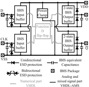
The figure 2 shows the simplified schematic of the integrated circuit built to evaluate system level ESD susceptibility. The model is built around the functionality of the chip described in VHDL language (“Function D flip-flop” center block).
Figure 2: Simplified integrated circuit model with ESD protection from measurement and input and output buffer from IBIS model The input and output buffer information is added to the VHDL-AMS model from the Input/Output Buffer Information Specification (IBIS) file [11]. The IBIS standard provides signal integrity designers with I(V) tables of buffers, V(t) tables for the dynamic output buffers, passive-elements of the package pins, input/output (I/O) equivalent capacitances (Ccomp) and others. The “2-state IBIS output buffer” blocks include the V(t) and I(V) curve of the pull-up and the pull-down of each output. A numerical signal from the core of the circuit allows triggering the output transitions. The “IBIS input buffer” blocks allow taking into account the threshold voltage levels that switch the component to high or low levels. To build these blocks the VIH and VIL from the datasheet
information is used and combined to IBIS.
Although the IBIS file gives tables of “ESD_clamps”, the ESD protection elements are based on TLP and static measurements and modeled into VHDL-AMS.. Note that in the IBIS standard, the structure called “power clamp” represents the structure between one I/O and VDD, and not
the protection between VDD and VSS as commonly used in
the ESD community.
(a) Diode (b) SCR
Figure 3: Example of the machine states describing the behavior of the ESD protection.
1) Extracting parameters from measurement
From quasi-static I(V) curves, behavioral models of the protections are built following machine state diagrams. Figure 3 gives the state machine example of a diode (a) and a SCR (b) extracted from the simplified reported characteristics. The main difficulty of such models is to fulfill the convergence of the simulator for strong discontinuities (like between state 1 and 2 of the SCR). This is overcome by adding in parallel to the protection structures the parasitic capacitances given by IBIS form each I/O. This is fully detailed in [17] and [18].
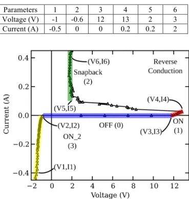
One TLP measurement example of the SCR-based ESD protection structure is given in figure 4. The inflexion points of the measured waveform are extracted as parameters to build the model. Six couples of voltage and current parameters (Vx, Ix) are needed to implement the full SCR model as reported in figure 4 and table 1. Four states, highlighted on the measurement, are identified: no conduction (0), reverse conduction before snapback (1), snapback (2), forward conduction (3). For each SCR states, a generic linear equation is used. The current I, and voltage V, are respectively the current flowing through and the voltage across the structure. The curve slope and the y-intercept are computed from parameters of table 1. For the SCR, four simultaneous equations, each defined by a state, must be solved. A simultaneous “If” statement structure is used to switch from one equation to the other.
Change-equation conditions could be defined by two ways. For simple structures, such as a diode, condition could be directly defined in the analog solver on voltage or current level. In this case, only the analog core is used. This kind of condition does not permit to model a structure such as a
SCR. The main difficulty with SCR is the modeling of the discontinuity when it goes into snapback states. To define more complex change states conditions, the digital core of the VHDL-AMS simulator is used as explained in the next section.
TABLE I.
SCR PARAMETER EXTRACTION FROM QUASI-STATIC CURVE
Parameters 1 2 3 4 5 6
Voltage (V) -1 -0.6 12 13 2 3 Current (A) -0.5 0 0 0.2 0.2 2
Figure 4: Quasi-static (TLP) measurement of a SCR protection structure. 2) Using the Digital Core for State machine
This section describes how to define the change state conditions for the model using the digital core. As a starting point, a state diagram is developed to define the release statement conditions of the SCR (figure. 3b), in which all the changes are reported. Moving from State 0 to State 1 implies that the voltage across the SCR must be higher than V3 defined by the parameter number 3 in Table 1. Reciprocally, to move from state 1 to state 0, the voltage across the SCR must be lower than V3. An access to a state can only be defined in one way. When the voltage V is above V4, the state switches to state 2 (snapback). However, no return condition is defined between state 2 and 1. The SCR can leave state 2 only to switch to state 0. A digital signal used as flag allows indicating to the analog solver the state of the SCR as indicated in figure 5. It is updated each time the process ends. This flag is used as condition in the “If” statement of analog core. The VHDL-AMS source file corresponding to the SCR is reported in figure 6.
Figure 5: Process organization chart.
The main advantage of this method is that it is possible to model complex ESD functionalities such as the discontinuity induced by the snapback of a structure. Moreover, VHDL-AMS allows complex interactions such as the derivation for the modeling of active ESD structure. Using simple information, such as six I/V points for SCR structures, it is easy to build behavioral models for ESD system level simulation. Before using full behavioral models, semi-physical models have been investigated in [14]. The same results have been obtained with a significant decrease in computation time for the behavioral models.
Figure 6: VHDL-AMS SCR description.
3)
Circuit modeling from IBIS and Behavioral ESD Protection ModelThe circuit studied here includes diodes from ground to outputs and outputs to VDD, SCR between inputs and
ground, and a power clamp between VDD and GND. From
TLP measurement, it is impossible to determine the actual design of the power clamp, but the IBIS behavioral description makes appear that the structure triggers on dV/dt. So in our VHDL-AMS model, the I(V) curve looks like the characteristic of a diode, but the triggered condition is defined by the VHDL command “V’dot>0.1e9”. The
figures 7 a and b report the simplified I(V) curves and the state diagram machine respectively.
(a) Simplified I(V) characteristic
(b) State machine diagram
Figure 7: Characteristic and state machine diagram used for the behavioral description of the Power Clamp.
Finally the parasitic elements of the package and the input and output capacitances provided by the IBIS file are added. The “IBIS Input Buffer” defines the High-level and Low-level input voltage (VIH and VIL), extracted from the
datasheet, proportional to VDD-VSS. The function of the
circuit core, represented in grey on figure 2, is described in VHDL. The new circuit model following the modeling methodology allows analyzing the system behavior circuit during an ESD disturbance.
B. Comparison of the measurement data and the simulation results
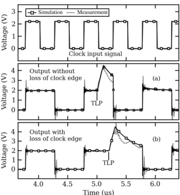
The measurement and simulation are performed with a 50nF external decoupling capacitor between VDD and ground, and a 75V TLP injection. The clock input frequency is 2MHz. Figure 8 shows the comparison of measurements and simulations in two cases (a) and (b). In configuration (a), the ESD disturbance occurs far from the clock synchronization point, which is the rising edge of the clock pulse. The output signal is still operating normally even if a strong disturbance is observed on the output signal.
In configuration (b), the ESD event takes place at the time when the clock synchronization occurs and is not taken into account by the D flip-flop. The output voltage remains at a high level and one period of the input signal is lost. More details about the failure mechanisms are given in section IV-B.
As shown on Figure 8, the simulation matches the measurements. Our modeling approach allows predicting what happens during an ESD event, specifically the analysis of the circuit behavior interaction with the system. A similar case that could introduce some failures is when the perturbation occurs close to the synchronization signal whereas the output is at low level.
As in the previous case, clock synchronization is lost. Measurement and simulation related to this case are reported in Figure 9. The simulation shows that the output keeps at a low level after the ESD stress. The simulation was not able to reproduce the observed noise close to the synchronization signal.
Figure 8: Transient measurements and simulations of the output voltage for configuration (a) and (b).
Figure 9: Transient simulations of the output voltage when the ESD stress occurs on a low level of the output.
IV. PROBABILITY A. Measurements of susceptibility failures
Measurement of failure probability has been performed regarding the external decoupling capacitor value (50nF and 6,8nF), the operational clock frequency (2, 5 and 10Mhz) and the ESD pulse amplitude (10 to 200V pre-charge voltage). Each TLP amplitude was repeated a hundred times. The TLP pulse is repeated every two seconds to avoid possible charge effects. All the results are computed and the percentage of failures is extracted and reported in Figure 10. For the low capacitor value and for
high operating frequency, the probability to generate failures is increased.
Figure 10: Evolution of the failure probability as a function of the external decoupling capacitance (Cdec), the clock frequency and the ESD pulse
amplitude B. Analysis
To simplify the situation as much as possible we start by considering the electrical schematic (fig 1). For this system we will only take into account the IC and its ESD protection between VDD and ground and the decoupling capacitor Cdec. Let us consider the case where the voltage
across the decoupling capacitor does not reach the triggering value of the protection.
A transition on the output occurs when a rising edge on the CLK signal is detected. The triggered input voltage, VIH, of the CLK signal is given by the datasheet as VIH = 0.7*VDD. When the TLP stress occurs, the internal power supply bus voltage increases as the external decoupling capacitor Cdec and the VIH of the clock do. Two cases have
to be considered: if the VIH level is lower than the clock input signal, the output switches to low-state (configuration a); if VIH is higher than the clock input signal it is not detected (configuration b). In the case displayed in figure 8, VIH reaches the value of 3.15V when VDD reaches 4.5V while the clock signal is between 0 and 2.2V. If the clock signal appears while VIH is higher than 2.2V it will not be taken into account. This occurs if VDD is higher than 3.15V, which will be defined as the critical power supply value Vcrit.
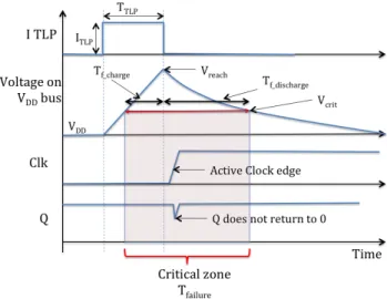
Let us assume that, as reported in Figure 11, a failure is generated if a clock event occurs while the power supply is over Vcrit during a fixed time (Tfailure). So the probability to
generate a failure is:
(1) Where Tclk_cycle is the synchronization clock cycle.
Figure 11: Chronograms showing the signal evolution during the ESD TLP stress.
To estimate (in a first approximation) this probability, we have to formulate Tfailure, which is the sum of Tf_charge and
Tf_discharge. Tf_charge, is the time during which the power
supply voltage exceeds Vcrit corresponding to the capacitor
charge and Tf_discharge is the time during which the power
supply voltage exceeds Vcrit corresponding to the capacitor
discharge.
1) 1. Estimation of Tf_charge:
Since the increase of VDD during the TLP pulse (TLP
amplitude = ITLP, and TLP duration = TTLP) is forced by the
external capacitance Cdec, we can use the basic equation (2).
(2) Vcrit is reached at the time :
(3) If Vreach is over Vcrit. Then Tf_charge is defined by
Tf_charge = TTLP – Tcrit (4)
2) Estimation of Tf_discharge:
The discharge is more complex because the only discharge path goes through the IC via its Pull-Up transistor. The equivalent resistance, RPull_up, given by the IBIS files is
around 8 Ohms and so, the evolution of the discharge voltage, Vdisch is :
(5) where τ is the RPull_up . Cdec product. It results that Tf_discharge
is :
(6)
(7) Finally, the probability to generate a failure in this case is given by :
€
P
failure=
T
failureT
clk _ cycle!
I = C
dV
dt
€
t
crit=
(V
crit− V
DD).C
decI
TLP€
V
disch(t) = V
DD+ (V
reach− V
DD)e
− tτ€
T
f _ disch arg e= −τ.ln
V
crit− V
DDV
reach− V
DD$
%
&
'
(
)
€
T
f _ disch arg e= −τ.ln
(
V
crit− V
DD)
.C
decI
TLP.T
TLP− V
DD.C
dec$
%
&
&
'
(
)
)
(8) According to this set of equations, an error could happen as soon as Vcrit is higher than 2.2V in our configuration (TTLP
= 100 ns and Cdec = 50nF), i.e. when VDD>3.15V. The
minimum TLP pulse that could generate this perturbation is extracted from (2) which is the correct measured value:
i.e. VTLP > 52V
In Figure 12, equation (8) is plotted and compared to measurement data for Cdec=50nF. The probability fits
correctly for higher frequencies but not well when the amplitude of the stress increases.
When the amplitude of the TLP is high enough to cause the power supply bus VDD to reach the triggering value of the power clamp (7V), a part of the current goes through the ESD protection slowing the charge of the capacitor and reducing the probability of upset. The triggering voltage of the power clamp (PC) is reached for a TLP injection of :
(9)
Where Vth is the triggering voltage of the power clamp.
For the 50nF decoupling capacitance, Vth corresponds to ITLP=2.5A, i.e. 125V injection, and for the 6.8nF, to 0.37A,
i.e. 18V. In comparison to Figure 10, the chances in the probabilities seem to be in this range of about 100V for 50nF injected voltage. This validates the impact of the power clamp to reduce the probability of failure. But what happens when the injected TLP voltage increases?
Figure 12: Evolution of failure probability depending on external decoupling capacitance (Cdec = 50nF), clock frequency and ESD
pulse amplitude
Figure 13 displays the simulation waveforms of the internal VDD voltage, and the current through the PC for a 400V TLP injection. The results from two simulations are shown, one taking into account the PC and the second one without
the PC. It can be seen that the PC absorbs a great part of the injected current, up to 4,5A, limiting the maximum amplitude of the internal power supply to 11.6V instead of the 16.5V without the PC. This difference of about 5V between the two situations is significant. When the threshold voltage of the PC has been reached, the charge of the capacitor is reduced in a non-linear way. When the PC triggers on, the current is split in two: the PC sinks one part, its value being defined by the potential across the capacitor, the other part still charging the capacitor. When the TLP signal ends, the discharge is first accelerated by the conduction of the power clamp and then when the PC turns off it follows equation (6). Finally, the internal power supply voltage comes back to Vcrit 600 ns sooner with the PC than without the PC.
As a conclusion, the estimation of the failure probability should be split in two parts.
Part 1: if the internal power supply voltage stays below the triggering voltage of the power clamp (Vth), equation (8)
applies.
Part 2: if the internal power supply voltage exceeds the triggering voltage of the power clamp, a more complex equation has to be established, taking into account the current circulating into the power clamp. The failure probability continues to increase but in a slower way.
Figure 13 : Transient simulations of the current through the power clamp (PC) and of the internal VDD voltage (without the PC : black, and with the
PC : grey). V. CONCLUSION
The susceptibility of an IC configured as a simple D flip-flop is investigated and the impact of ESD stresses is investigated during system operation. The failure probability is addressed and linked to the parameters of the external decoupling capacitor, the operational frequency and the stress amplitude. The full simulation of the system is carried out using a behavioral description. The protection strategy has been extracted from quasi-static measurement. The functional core chip is described in VHDL, and I/Os buffers are introduced from IBIS description file. As shown in this paper, the behavior of the IC undergoing ESD events
€
P
failure=
T
failureT
clk _ cycle=
T
f _ ch arg e+ T
f _ disch arg eT
clk _ cycle€
I
TLP>
3.15 * C
dect
TLP€
I
TLP=
C
dec(V
th− V
DD)
T
TLPis predicted with a very good accuracy. Concurrently, a basic analysis has been conducted to define a simple formulation of the failure probability. A preliminary model based on a simple theory have been proposed and compared with measurement. The influence of the ESD protection on the evolution of the failure probability has been demonstrated but modeling improvement is still needed to establish a generic formulation.
ACKNOWLEDGMENT
This research was supported by ANR E-SAFE project. The authors would like to thank Michael Hopkins for reviewing this paper.
REFERENCES
[1] IEC 61000-4-2. Electromagnetic compatibility (EMC) – Part 4-2: testing and measurement techniques – electrostatic discharge immunity test. Ed 2.0, 2008-12. ISBN: 2-8318-1019-7.
[2] M. P. J. Mergens, M. T. Mayerhofer, J. A. Willemen, M. Stecher, ESD Protection Considerations in Advanced High-Voltage Technologies for Automotive, EOS/ESD
Symposium, 2006, pp.54-63.
[3] T. Smedes, J. Van Zwol, G. De Raad, T. Brodbeck, H. Wolf, “Relations Between System Level ESD and (vf-) TLP”, EOS/ESD Symposium, 2006, pp.136-143.
[4] M.Camp and al., “Influence of the Technology on the Destruction Effects of Semiconductors By Impact of EMP and UWB Pulses”, IEEE Symposium on Electromagnetic Compatibility, 2002, Vol: 1, pp. 87-92.
[5] O. Semenov, H. Sarbishaei, and M. Sachdev, “ESD protection device and circuit design for advanced CMOS technologies”. Springer Verlag, 2008, ISBN 978-1-4020-8300-6.
[6] W. Stadler, S. Bargstadt-Franke, T. Brodbeck, R. Gaertner, M. Goroll, H. Gosner, and C. Jensen, “From the ESD robustness of products to the system ESD robustness,” in Electrical Overstress/Electrostatic Discharge Symposium, 2004. EOS/ESD, 2004, pp. 1–8.
[7] W. Stadler, T. Brodbeck, R. Gaertner, and H. Gossner, “Do ESD fails in systems correlate with IC ESD robustness ?” Microelectronics Reliability, vol. 49, no. 9-11, pp. 1079– 1085,
[8] P. Besse, K. Abouda, and C. Abouda, “Identifying electrical mechanisms responsible for functional failures during harsh external ESD and EMC aggression,” Microelectronics Reliability, vol. 51, no. 9-11, pp. 1597–1601, 2011.
[9] N. Lacrampe, A. Boyer, F. Caignet, “Investigation of effects of an ESD pulse injected by a near-field probe into an oscillator block of a 16-bit microcontroller”, IEEE EMC Workshop 2007
[10] N. Lacrampe, A. Alaeldine, F. Caignet, R. Perdriau, , "Investigation on ESD Transient Immunity of Integrated Circuits," Electromagnetic Compatibility, 2007. EMC 2007. IEEE International Symposium July 2007.
[11] IBIS (Input Output Buffer Information Specification) ANSI/EIA-656B, www.eigroup.org/IBIS
[12] IEC62132-4: “Integrated circuits, Measurement of electromagnetic immunity – 150 kHz to 1 GHz - Part 4: Direct RF power injection method”
[13] T.Maloney et N.Khurana, "Transmission line pulsing techniques for circuit modeling of ESD phenomena", 7th EOS/ESD Symposium, p. 49-54, Minneapolis, MN, 1985 [14] N. Monnereau, F. Caignet, D. Tremouilles, "Building-up of
system level ESD modeling: Impact of a decoupling capacitance on ESD propagation," Electrical Overstress/ Electrostatic Discharge Symposium (EOS/ESD), 2010 32nd, 3-8 Oct. 2010
[15] M. Honda, "Measurement of ESD-gun radiated fields," 29th Electrical Overstress Electrostatic Discharge Symposium, 2007. EOS/ESD
[16] D. Lin, D. Pommerenke, J. Barth, L. G. Henry, H. Hyatt, M. Hopkins, G.Senko, D. Smith, “Metrology & methodology of system level ESD testing,” EOS / ESD Symposium Proc., 1998, pp. 29-39.
[17] P. Besse, F. Lafon, N. Monnereau, F. Caignet, J.P. Laine, A. Salles, S. Rigour, M. Bafleur, N. Nolhier, D. Tremouilles, "ESD system level characterization and modeling methods applied to a LIN transceiver" Electrical Overstress/
Electrostatic Discharge Symposium (EOS/ESD), 2011 33nd , vol., no., pp….Oct. 2011
[18] N. Monnereau, F. Caignet, N. Nolhier, D. Trémouilles, M. Bafleur, " Behavioral-Modeling Methodology to Predict Electrostatic-Discharge Susceptibility Failures at System Level : an IBIS Improvement" EMC Europe Symposium sept. 2011.