HAL Id: cea-01520354
https://hal-cea.archives-ouvertes.fr/cea-01520354
Submitted on 10 May 2017HAL is a multi-disciplinary open access archive for the deposit and dissemination of sci-entific research documents, whether they are pub-lished or not. The documents may come from teaching and research institutions in France or abroad, or from public or private research centers.
L’archive ouverte pluridisciplinaire HAL, est destinée au dépôt et à la diffusion de documents scientifiques de niveau recherche, publiés ou non, émanant des établissements d’enseignement et de recherche français ou étrangers, des laboratoires publics ou privés.
Angle dependence of the local electronic properties of
the graphene/MoS_2 interface determined by ab initio
calculations
Daniela Di Felice, Enrique Abad, Cesar Gonzalez Pascual, Alexander
Smogunov, Yannick Dappe
To cite this version:
Daniela Di Felice, Enrique Abad, Cesar Gonzalez Pascual, Alexander Smogunov, Yannick Dappe. Angle dependence of the local electronic properties of the graphene/MoS_2 interface determined by ab initio calculations . Journal of Physics D: Applied Physics, IOP Publishing, 2017, 50, pp.17LT02. �10.1088/1361-6463/aa64fe�. �cea-01520354�
This content has been downloaded from IOPscience. Please scroll down to see the full text.
Download details:
IP Address: 132.166.160.12
This content was downloaded on 11/05/2017 at 13:08
Please note that terms and conditions apply.
Angle dependence of the local electronic properties of the graphene/MoS2 interface
determined by ab initio calculations
View the table of contents for this issue, or go to the journal homepage for more 2017 J. Phys. D: Appl. Phys. 50 17LT02
(http://iopscience.iop.org/0022-3727/50/17/17LT02)
Home Search Collections Journals About Contact us My IOPscience
You may also be interested in:
Electronic properties of MoS2 sandwiched between graphene monolayers Li Shao, Guangde Chen, Honggang Ye et al.
Theoretical characterisation of point defects on a MoS2 monolayer by scanning tunnelling microscopy C González, B Biel and Y J Dappe
Lattice match and lattice mismatch models of graphene on hexagonal boron nitride from first principles
Xiaoyang Zhao, Linyang Li and Mingwen Zhao
Band engineering of the MoS2/stanene heterostructure: strain and electrostatic gating Wenqi Xiong, Congxin Xia, Juan Du et al.
Modification of the electronic properties of hexagonal boron-nitride in BN/graphene vertical heterostructures
Minghu Pan, Liangbo Liang, Wenzhi Lin et al.
Controllable Schottky barrier in GaSe/graphene heterostructure: the role of interface dipole Chen Si, Zuzhang Lin, Jian Zhou et al.
Van der Waals stacked 2D layered materials for optoelectronics Wenjing Zhang, Qixing Wang, Yu Chen et al.
Bottom-up fabrication of graphene nanostructures on Ru(1010) Junjie Song, Han-jie Zhang, Yiliang Cai et al.
1 © 2017 IOP Publishing Ltd Printed in the UK Journal of Physics D: Applied Physics
D Di Felice et al
Angle dependence of the local electronic properties of the graphene/MoS2 interface determined by ab initio calculations
Printed in the UK
17LT02 JPAPBE
© 2017 IOP Publishing Ltd 50
J. Phys. D: Appl. Phys.
JPD
10.1088/1361-6463/aa64fe
17
Journal of Physics D: Applied Physics
Since the discovery of graphene [1, 2], which is a two- dimensional (2D) material made of a single layer of carbon atoms, a huge amount of research has been devoted to the exploration of new 2D materials. Their electronic properties range from semiconductors to metals, like hexagonal boron nitride [3], fluorographene or transition metal dichalcogenide (TMDC) [4, 5]. Among these, molybdenium disulfide (MoS2) has very interesting electronic properties, being a semiconduc-tor with an indirect gap in its multilayer phase, which turns into
a direct gap in the monolayer phase [6, 7]. As suggested by Geim et al [8], another interesting property of 2D materials is their combination through vertical van der Waals (vdW) heter-ostructures. In this way, it is suggested that the electronic prop-erties of each layer should be conserved, resulting in the Fermi level alignment of all the structures. Consequently, the poten-tial combination of different 2D materials which are bonded through vdW interactions can lead to benefits from the elec-tronic properties of each sheet, opening promising perspectives for future nanoelectronic devices. For example, the graphene/ MoS2 interface has been considered for transistor design, mak-ing use of the high conductivity of graphene, and the elec-tronic gap of MoS2 to achieve a potential barrier in the system [9–13]. However, the interaction between graphene and MoS2
Angle dependence of the local electronic
properties of the graphene/MoS
2
interface
determined by ab initio calculations
D Di Felice1, E Abad2, C González1,3, A Smogunov1 and Y J Dappe1,41 SPEC, CNRS, CEA, Université Paris-Saclay, 91191 Gif-Sur-Yvette, France 2 German Research School for Simulation Sciences GmbH 52425, Jülich, Germany
3 Departamento de Electrónica y Tecnología de Computadores, Universidad de Granada, Campus de
Fuente Nueva & CITIC, Campus de Aynadamar E-18071 Granada, Spain E-mail: yannick.dappe@cea.fr
Received 19 December 2016, revised 3 March 2017 Accepted for publication 7 March 2017
Published 28 March 2017
Invited by Board Member Patrick Soukiassian Abstract
We present a full theoretical study of the graphene/MoS2 interface, using density functional theory (DFT) calculations and scanning tunneling microscopy (STM) simulations. In particular, we show that contrary to previous theoretical predictions, the rotation angle between the layers has no influence on the global electronic properties of the interface, providing a careful choice of lattice vectors and supercells is made, in order to avoid artificial modifications in the electronic structure. However, small modifications of the local electronic properties do appear, as revealed by the calculated STM images. This result might be exploited in nanoelectronic devices by specific local contacting.
Keywords: graphene/MoS2, DFT, STM, vdW heterostructures, electronic structure S Supplementary material for this article is available online
(Some figures may appear in colour only in the online journal)
Letter
IOP
Original content from this work may be used under the terms of the Creative Commons Attribution 3.0 licence. Any further distribution of this work must maintain attribution to the author(s) and the title of the work, journal citation and DOI.
2017
1361-6463
4 Author to whom any correspondence should be addressed.
1361-6463/17/17LT02+6$33.00
https://doi.org/10.1088/1361-6463/aa64fe J. Phys. D: Appl. Phys. 50 (2017) 17LT02 (6pp)
2 does not seem to be clear yet [14]. As such, several theoretical and experimental papers have exhibited the specific modifica-tion of graphene and MoS2 electronic properties, according to the specific rotation angles between the layers [15–18]. From a theoretical point of view—except in the case of some specific rotation angles, for which the mismatch between the single layer lattices is compensated exactly—the optimization of the supercell using periodic boundary conditions results in an equilibrium structure characterized by an artificial strain on both the graphene and MoS2. The strain on MoS2 or gra-phene has an important effect on its electronic properties, in particular affecting the value and type of energy band gap [19]. For example, in their optimized structure, Yandon Ma
et al [20] found a small band gap opening in the Dirac cone of graphene of some meV that increases as the interlayer dis-tance is reduced. More recently Ebnonnasir et al [21] found a dependence of the MoS2 thickness with respect to the orienta-tion between the constituent layer, affecting the value and the type of the semiconductor energy band gap. In this work, we consider the different rotation angles between graphene and MoS2, in order to elucidate the mutual influence between the two monolayers. We first discuss the structural aspects of the graphene/MoS2 interfaces, namely the unit cells for the density functional theory (DFT) calculations considered for the differ-ent rotation angles and the corresponding interaction energies. Then we analyze the electronic band structures and density of states (DOS), and finally we present the simulated scan-ning tunneling microscopy (STM) image calculations, which exhibit different Moiré patterns for the different structures.
Our calculations have been performed using the localized orbital DFT-Fireball code [22, 23], which includes a specific treatment of vdW interactions [24]. In addition, a scissor operator has been used for electronic level alignment correc-tions [25, 26]. This operator is introduced in the Hamiltonian in order to correct for the misalignment between graphene and MoS2. This misalignment is a result of the small size of the basis set used in our calculations. By virtue of this operator, we can rigidly shift the band of one system with respect to the
other and obtain the correct energy level alignment of both systems using our very efficient basis set. In particular, if we want to shift the band εα( )k by the value ∆α( )k, we can write
the scissor operator as:
( )∣ ( )⟩⟨ ( )∣
∑
α α = ∆ α α OS k k k k , (1) where ∣ ( )⟩α k is the eigenorbital with energy εα( )k. A detailed mathematical derivation of the scissor operator matrix elements on a numerical atomic orbital basis set can be found in the supplementary information (see stacks.iop.org/JPhysD/50/17LT02/mmedia). The STM images are calculated within a Keldysh–Green function for-malism using the Hamiltonian obtained in the Fireball simulation [27–29]. Full details of the method are provided in the supple-mentary information. As is well known in the theoretical design of material interfaces, due to the periodic conditions imposed in DFT to reproduce an infinite interface, a common basis of lattice vectors for the new superstructure composed by the rotation of one material with respect to the other has to be found [30]. Therefore, considering an n×n unit cell of graphene and an m×m unit cell of MoS2, the indices n and m are related by the following equation:( )θ = na1 mb1cos (2) where a→ 1 and →
b1 are the lattice vectors of the isolated
gra-phene and the MoS2 unit cells respectively, and θ is the rota-tion angle of one layer with respect to the other. However, the perfect matching of both structures is almost impossible to obtain, making DFT calculations impractical. As a conse-quence, the relative matching of the two structures in the new superstructure can be obtained, inducing a necessarily small error in the optimization process. Indeed, depending on the lattice vector used, namely na1 or mb1cos( )θ, the structures
relax differently in most cases. This induces artificial strain and corrugation that lead to changes in the electronic proper-ties of the deformed material at the interface. As an attempt to overcome this difficulty, we have designed supercells with reasonable numbers of atoms for the DFT calculations, favor-ing optimization along one material lattice vector or the other.
d
C-S(Å)
MoS2lvs graph lvs 5d
C-S(Å)
d
C-S(Å)
d
C-S(Å)
I.E.(meV/
Å
2)
5I.E.(meV/Å
2)
0 -5 -10 -15 -20 -25 2.5 3.0 3.5 4.0 4.5 5I.E.(meV/Å
2)
0 -5 -10 -15 -20 -25 2.5 3.0 3.5 4.0 4.5 5I.E.(meV/Å
2)
0 -5 -10 -15 -20 -25 2.5 3.0 3.5 4.0 4.5a)
b)
c)
d)
0 -5 -10 -15 -20 -25 2.5 3.0 3.5 4.0 4.5Figure 1. A representation of the calculated interaction energies of the graphene/MoS2 interfaces for (a) 0, (b) 10, (c) 20 and (d) 30 degrees,
as a function of the average carbon-sulfur distance. The black (red) curves are related to the optimization along the MoS2 (graphene) lattice
vectors. The corresponding geometries for graphene or MoS2 lattice vectors are represented in the top and bottom insets, respectively. The
gray, yellow and blue spheres correspond to carbon, sulfur and molybdenum atoms, respectively. J. Phys. D: Appl. Phys. 50 (2017) 17LT02
3 Our criterium for designing the cell is that the lateral distance between the matching atoms of the different planes should not exceed 0.5 Å. In this way, we can observe the differences in the electronic properties induced by the calculation condi-tions, and remove them from the possible physical effects at the interface. According to their corresponding lattice vectors, these different structures have then been optimized and the equilibrium distance between the two layers is determined, making use of the LCAO-S2 + vdW formalism implemented in the Fireball code [24]. The corresponding interaction energy curves as a function of the average carbon-sulfur distance between the graphene and MoS2 are represented in figures 1 (a)–(d). The geometries of the unit cell designed for each angle and for the graphene or MoS2 lattice vectors are represented in the insets.
Except for the 0 degree structure, there is no noticeable difference between the interaction energies corresponding to the optimization, either with the graphene or the MoS2 lattice vectors. In all the structures, the interaction energy is around 22 meV A˚−2. This value is a bit lower than the one found for
the AB stacking of graphene, which is around 40 meV A˚−2, calculated using the same formalism. This smaller interaction energy can be explained by the honeycomb structure of MoS2, composed of alternating sulfur and molybdenium atoms, with the last kind in a lower plane. Consequently, the molybdenium atoms are located farther from the graphene plane, which reduces the overall interaction energy with the graphene sheet. Regarding the 0 degree graphene/MoS2 interface, which is composed of a 3×3 MoS2 and a 4×4 graphene unit cell, this superstructure presents the most important strain after optim ization, either for graphene with a 3.1 % extension in the MoS2 lattice vectors, or for MoS2, with a 2.8 % compres-sion in the graphene lattice vectors. As a consequence of this important strain, the graphene plane presents a larger corruga-tion which is responsible for the energy difference between the two lattice vector optimizations. Since there is no signifi-cative difference in the other rotation angles, we can deduce that the interaction energy mainly depends on the strain and the graphene corrugation. Regarding the equilibrium distance, defined as an average distance for the corrugated system, in
Table 1. Evolution of the C–C distance in graphene, the MoS2 lattice parameter, the strain and the corrugation for 0, 10, 20 and 30 degrees
according to the corresponding lattice vector optimization, either for graphene (Gr) or MoS2. A positive strain corresponds to a compression
whereas a negative strain corresponds to an extension of the layer.
Angles 0 10 20 30
Lattice vector MoS2 Gr MoS2 Gr MoS2 Gr MoS2 Gr
dC–C (Å) 1.39 1.43 1.41 1.43 1.40 1.43 1.42 1.43 aMoS2 (Å) 3.20 3.30 3.20 3.24 3.20 3.27 3.20 3.22 Strain (%) −2.8 on Gr +3.1 on MoS2 −1.4 +1.2 −2.1 +2.2 −0.7 +0.5 Corrugation (Å) 0.53 0.14 0.11 0.08 0.03 0.03 ⩽0.03 ⩽0.03
E-E
F(eV)
3
2
1
0
-1
-2
-3
E-E
F(eV)
DOS(a.u.)
DOS(a.u.)
20 0 40a)
b)
c)
d)
e)
f)
g)
h)
E-E
F(eV)
-3 -2 -1 0 1 2 3E-E
F(eV)
-3 -2 -1 0 1 2 3E-E
F(eV)
-3 -2 -1 0 1 2 3DOS(a.u.)
Γ
K M
Γ
K M
Γ
K M
Γ
K M
3
2
1
0
-1
-2
-3
3
2
1
0
-1
-2
-3
3
2
1
0
-1
-2
-3
E-E
F(eV)
E-E
F(eV)
E-E
F(eV)
30 20 10 0 -3 -2 -1 0 1 2 3 150 100 50 0DOS(a.u.)
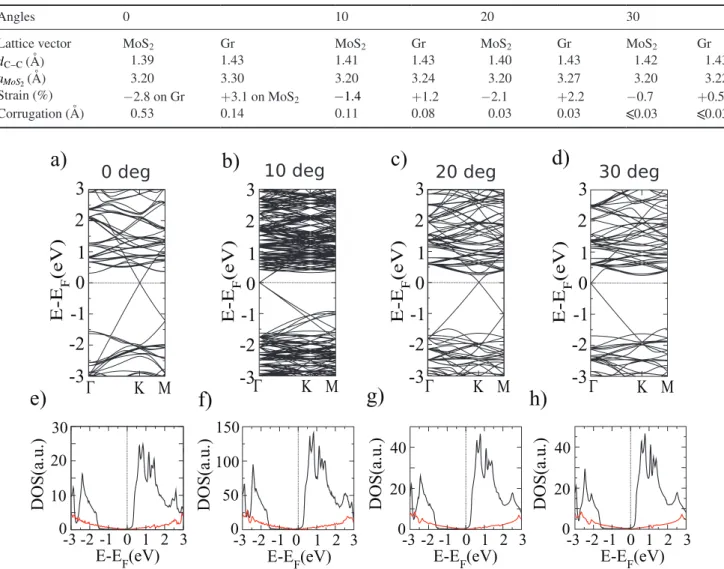
20 0 40Figure 2. Electronic band structures and DOS for MoS2 (black line) and graphene (red line), without the scissor operator for 0 degrees
(a) and (e), 10 degrees (b) and (f ), 20 degrees (c) and (g), 30 degrees (d) and (h) in the MoS2 lattice vector optimization.
4 all cases it remains almost constant at 3.1 Å, independently of strain or corrugation. The main structural characteristics for the different rotation angles are summarized in table 1.
The calculated electronic structure of the previous configu-rations shows that the optimization with respect to different lattice vectors leads to rather different electronic properties in the equivalent unit cells. At 0 degrees, in the lattice vector optimization of graphene, the MoS2 band gap is substantially reduced from 1.83 eV to 1.1 eV, and the bottom of the conduc-tion band is located right at the Fermi level (see figure S2 in the supplementary information). We can also observe a small amount of p-doping in graphene, as the Dirac point is shifted above the Fermi level. This is related to the very important artificial strain on the MoS2 layer, favoring an important charge transfer from graphene to MoS2. Since the same strain on graphene does not show any important effect on the elec-tronic structure, we will consider the MoS2 lattice optim-ization for the rest of the study, in order to avoid any artificial strain effects.
The band structure and the DOS for 0, 10, 20, 30 degrees are represented in figure 2. For each angle, the Dirac point is now located at the Fermi level, as expected for the isolated graphene layer. Notice that the Dirac cone is mapped at the Γ
point for the 10 and 30 degree structures, due to the particular symmetry of the corresponding supercells. Indeed, as is well-known [31, 32], when an n×n supercell is considered, the corresponding Brillouin zone (Bz) is reduced by a factor of
×
n n. As a consequence, the k-points are re-mapped into the shrinked Bz by projection. This is the so-called Bz folding effect. While Γ is always located at the center of the Bz, the
other symmetry points (K and M in the hexagonal structure) can be projected in different points depending on the periodic-ity and the crystal structure of the supercell. In the specific case of a hexagonal crystal structure, when n is a multiple of 3, the K symmetry point is projected on Γ, as happens in our case for the 10 and 30 degree configurations.
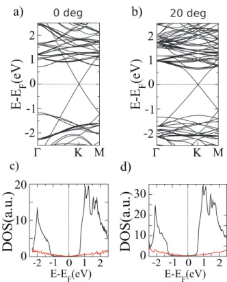
Also, the bottom of the MoS2 conduction band is now located at 0.3 eV above the Fermi level and the MoS2 band gap presents the same value for all the considered angles. Since the 20 and 30 degree configurations are made with the same number of MoS2 unit cells, a MoS2 band to band comparison does not reveal any band structure dependence on the orienta-tion. The similarity of the DOS for each configuration also demonstrates that the orientation does not affect the global electronic properties, which result in the simple superposition of the electronic properties of each single system, as suggested by Geim et al [8]. However, in these initial calculations, there is an electronic level misalignment that should be corrected. Using the 0 degree cell and comparing the level positions with respect to the isolated layers, we have defined a unique scissor potential that will be applied to all the angles considered here. For example, the scissor-corrected DOS and band structures for 0 and 20 degrees are represented in figure 3. It is impor-tant to notice that the MoS2 conduction band is now shifted to 0.7 eV, above the Fermi level.
We can thus conclude that the global electronic structure of the graphene/MoS2 interfaces is unaffected by the rotation angle. However, small modifications of the local electronic structures appear as the STM calculations reveal. The simu-lated images of graphene/MoS2 interfaces for 0 and 20 degrees within the scissor-correction approach are represented in figures 4(a) and (b) respectively. The applied voltage is +0.7
V in order to include the conduction band of MoS2.
As a first remark, even though the global electronic proper-ties remain the same, different Moiré patterns can be obtained for the STM images for each rotation angle. It is important to notice that the bright spots are placed on the hollow sites of the graphene sheet due to the large contribution of the non-directional d-orbitals in the tip (see the DOS of the W
2 1 0 2 1 2 1 0 1 2 E-EF(eV) E-EF(eV)
20
10
0
DOS(a.u.)
DOS(a.u.)
30
20
10
0
Γ
K M
2
1
0
1
2
2
1
0
1
2
Γ
K M
c)
a)
b)
d)
E-E
F(eV)
E-E
F(eV)
Figure 3. Electronic band structure and corresponding DOS for
MoS2 (black line) and graphene (red line), for (a) and (c) 0 degrees,
and (b) and (d) 20 degrees in MoS2 lattice vector optimization with
a scissor operator.
Figure 4. Calculated STM images of graphene/MoS2 for
(a) 0 degrees and (b) 20 degrees. In (c) and (d), the STM images calculated on isolated graphene, in the corresponding graphene/ MoS2 configuration.
5 tip in [27]) and the C–C distance reduction due to the gra-phene compression. These Moiré patterns have already been observed in ARPES experiments for example, as a mini-gap opening in the global band-structure of the interface [33]. As the electronic structure of the C atoms is almost unaltered, the difference in the brightness of the spots is directly linked to the corrugation in the graphene sheet. For example, the Moiré pattern for the 0 degree unit cell exhibits a large black area around the C-atoms in the lower position—i.e. the hollow site with a S atom below—while the brightest sites correspond to the coincident points where a C atom of the graphene sheet falls over a S atom of the MoS2 layer. In order to check the effect of the MoS2 layer in the current, in figures 4(c) and (d) we represent the STM image for an isolated graphene plane in the configuration of the graphene/MoS2 interface for 0 and 20 degrees, respectively. The main features of the gra-phene/MoS2 STM image are caught by the image of the iso-lated graphene layer, but less defined spots are obtained. This result means that there is a modulation effect in the image due to the inclusion of the MoS2 layer. The STM images of the other cells show a less pronounced contrast between the brightest and the darkest areas due to the lower corrugation. As illustrated in figure S3, the corrugation decreases as the rotation angle is increased (up to 30 degrees). Also notice that the corrugation is mainly due to the interaction between graphene and MoS2, since we have checked that the isolated graphene monolayer remains flat even in the most corrugated case (see supplementary information for more details on cor-rugation). On the other hand, the graphene-MoS2 interaction is reflected in the STM image change when the MoS2 under-layer is removed (compare images in figures 4(a), (c) and (b), (d)). Finally, the images calculated in the gap of MoS2, i.e. at −0.1 V, (see figure S4), present the bright spots over the C atoms of graphene, exhibiting a lower contrast. In that respect, graphene acts as a grid for the MoS2 electronic structure.
We have also calculated the charge transfer between the two layers, which is very small, in agreement with the unaf-fected electronic structure with the rotation angle. As a con-sequence of these results, the electronic device seems to be unaffected by the inclusion of graphene/MoS2 interfaces with different rotation angles. However, their local electronic property modifications can be exploited through specific con-nections to the area with high or low electronic density. To illustrate this feature, we have calculated the conductance variation when approaching an STM tip to a black or white area in the 0 degree graphene/MoS2 interface. As represented in figure S5 (supplementary information), we can observe significative differences in the corresponding conductance. These results, however, present small differences from some experimental results, where the stretch of one of the 2D mat-erials [34] or band bending [35] have been observed at such interfaces, modifying the global electronic properties of the system. Here, we propose a tentative explanation for this slight discrepancy; however, without any calculation data for the moment. This will be the goal of a full future work on lat-eral interfaces between 2D materials. Theoretically, the inter-face is composed of two infinite planes, which implies full
vdW interaction between the two structures. However, exper-imentally, a graphene/MoS2 interface is usually composed of MoS2 triangles deposited on graphene, which therefore pre-sent connections at the border, whose nature is slightly differ-ent from vdW interactions. Indeed, the triangle edges presdiffer-ent dangling bonds which are much more reactive than the π
orbit-als involved in the weak vertical interaction. Consequently, we think that the main difference between experiment and theory in the structural and electronic behavior of vdW het-erostructures might arise from those dangling bonds forming a lateral heterostructure between MoS2 and graphene, and not weak horizontal heterostructures. A future work will then be devoted to the study of such heterojunctions, in order to esti-mate their weight in the experimentally measured vdW het-erostructures between 2D materials.
To summarize, we have presented a full study of the influ-ence of the rotation angle on the electronic properties of the graphene/MoS2 interface. As a result, the global electronic structure remains unaffected by the rotation, even though calcul ations have to be conducted with a careful choice of lattice vectors and supercells to avoid artificial effects. For example, Yandong Ma et al [20] have theoretically demon-strated the small gap opening in the graphene band-structure for a specific rotation angle at the graphene/MoS2 interface, which might be due to the strain induced by the choice of the supercell and the corresponding lattice vectors. The rotation angle, however, has an influence on the local electronic prop-erties through the different Moiré patterns observed in the cal-culated STM images. These findings can be important in the design of future nanoelectronic devices employing the local contacting of vdW heterostructures.
Acknowledgment
D Di Felice thanks the CEA PHARE Program for funding her research. CG acknowledges funding by the Junta de Andalucía and the European Commission under the Co-funding of the 7th Framework Program in the People Program through the Andalucía Talent Hub program.
References
[1] Novoselov K S, Geim A K, Morozov S V, Jiang D, Zhang Y, Dubonos S V, Grigorieva I V and Firsov A A 2004 Science 306 666
[2] Novoselov K S et al 2012 Nature 490 192
[3] Jin C, Lin F, Suenaga K and Iijima S 2009 Phys. Rev. Lett. 102 195505
[4] Mas-Ballesté R, Gómez-Navarro C, Gómez-Herrero J and Zamora F 2011 Nanoscale 3 20
[5] Butler S Z et al 2013 ACS Nano 7 2898 [6] Conley H J et al 2013 Nano Lett. 13 3626
[7] Castellanos-Gomez A et al 2013 Nano Lett. 13 5361 [8] Geim A K and Grigorieva I V 2013 Nature 499 419
[9] Du Y, Yang L, Zhang J, Liu H, Majumdar K, Kirsch P D and Ye P D 2014 IEEE Electron Device Lett. 35 599
[10] Chanana A and Mahapatra S 2016 J. Appl. Phys. 119 014303 [11] Desai S B et al 2016 Science 354 99
6 [12] Qiu D and Kim E K 2015 Sci. Rep. 5 13743
[13] Myoung N, Seo K, Lee S J and Ihm G 2013 ACS Nano 7 7021–7
[14] Wan W et al 2016 RSC Adv. 6 323–30
[15] Liu X and Li Z 2015 J. Phys. Chem. Lett. 6 3269
[16] Jin C, Rasmussen F A and Thygesen K S 2015 J. Phys. Chem. C 119 19928
[17] Jin W et al 2015 Phys. Rev. B 92 201409
[18] Diaz H C, Avila J, Chen C, Addou R, Asensi M C and Batzil M 2015 Nano Lett. 15 1135–40
[19] Wang Z, Chen Q and Wang J 2015 J. Phys. Chem. C 119 4752 [20] Ma Y, Dai Y, Guo M, Niu C and Huang B 2011 Nanoscale
3 3883–7
[21] Ebnonnasir A, Narayanan B, Kodambaka S and Ciobanu C V 2014 Appl. Phys. Lett. 105 031603
[22] Lewis J P et al 2011 Phys. Status Solidi b 248 1989
[23] Jelínek P, Wang H, Lewis J P, Sankey O F and Ortega J 2005
Phys. Rev. B 71 235101
[24] Dappe Y J, Ortega J and Flores F 2009 Phys. Rev. B 79 165409
[25] Abad E, Martínez J I, Ortega J, Flores F 2010 J. Phys.:
Condens. Matter22304007
[26] Abad E 2013 Energy Level Alignment and Electron Transport
Through Metal/Organic Contacts (Heidelberg: Springer) (https://doi.org/10.1007/978-3-642-30907-6)
[27] González C, Abad E, Dappe Y J and Cuevas J C 2016
Nanotechnology27 105201
[28] González C, Biel B and Dappe Y J 2016 Nanotechnology 27 105702
[29] Sánchez-Sánchez C, González C, Jelinek P, Méndez J, de Andres P L, Martín-Gago J A and López M F 2010
Nanotechnology21 405702
[30] Lopes dos Santos J M B, Peres N M R and Castro Neto A H 2007 Phys. Rev. Lett. 99 256802
[31] Ku W, Berlijn T and Lee C-C 2010 Phys. Rev. Lett. 104 216401
[32] Gong L, Xiu S L, Zheng M M, Zhao P, Zhang Z, Liang Y Y, Chen G and Kawazoe Y 2014 J. Mater. Chem. C 2 8773 [33] Pierucci D et al 2016 Nano Lett. 16 4054
[34] Ben Aziza Z, Henck H, Di Felice D, Pierucci D, Chaste J, Naylor C H, Balan A, Dappe Y J, Charlie Johnson A T and Ouerghi A 2016 Carbon 110 396
[35] Zhang C, Johnson A, Hsu C-L, Li L-J and Shih C-K 2014
Nano Lett.14 2443 J. Phys. D: Appl. Phys. 50 (2017) 17LT02