HAL Id: tel-01714993
https://tel.archives-ouvertes.fr/tel-01714993
Submitted on 22 Feb 2018HAL is a multi-disciplinary open access archive for the deposit and dissemination of sci-entific research documents, whether they are pub-lished or not. The documents may come from
L’archive ouverte pluridisciplinaire HAL, est destinée au dépôt et à la diffusion de documents scientifiques de niveau recherche, publiés ou non, émanant des établissements d’enseignement et de
photonic structures
Dam Thuy Trang Nguyen
To cite this version:
Dam Thuy Trang Nguyen. Controlled coupling of nanoparticles to polymer-based photonic structures. Polymers. Université Paris Saclay (COmUE), 2018. English. �NNT : 2018SACLN014�. �tel-01714993�
Controlled coupling of
nanoparticles to polymer-based
photonic structures
Thèse de doctorat de l'Université Paris-Saclay préparée à l'Ecole normale supérieure Paris-Saclay
École doctorale n°575 EOBE Spécialité de doctorat: physique
Thèse présentée et soutenue à Cachan, le 26/01/2018, par
Dam Thuy Trang NGUYEN
Composition du Jury : Jean-Pierre Hermier
Professeur, Université de Versailles
Saint-Quentin-en-Yvelines (UMR 8635) Président
Manh-Huong Phan
Associate Professor, University of South Florida Rapporteur
Sophie Brasselet
Directrice de recherche, Université d'Aix-Marseille (UMR 7249) Rapporteur
Catherine Schwob
Professeur, Université Paris VI (UMR 7588) Examinateur
Isabelle LEDOUX-RAK
Professeur, ENS Paris-Saclay (UMR 8537) Examinateur
Ngoc Diep Lai
Maître de Conférences, ENS Paris-Saclay (UMR 8537) Directeur de thèse
NNT : 2 0 1 8 S A CLN 014
Dans ce travail, nous étudions théoriquement et expérimentalement le couplage en-tre nanoparticules uniques de différentes natures (fluorescentes, non-linéaires, plas-moniques, etc.) et une structure photonique en matériau polymère. Dans un premier temps, nous avons optimisé la méthode dite écriture directe par laser en régime de faible absorption à un photon (LOPA) pour réaliser des structures photoniques de bonne qualité à la demande. Ensuite, nous avons également exploité l’effet thermique induit par le laser d’excitation continue, pour simplifier la méthode de fabrication LOPA et améliorer les structures fabriquées. Puis nous avons introduit de façon précise une nanoparticule unique à un emplacement contrôlé dans la structure pho-tonique. Le couplage nanoparticule/structure photonique a été réalisé par le même système optique. Ce couplage a été démontré par une augmentation du nombre de photons émis par la nanoparticule fluorescente et par une forte amélioration du signal de génération de seconde harmonique. Parallèlement, nous avons effectué des calculs numériques par la méthode FDTD pour prédire les propriétés optiques intéressantes des structures photoniques et pour confirmer les résultats expérimentaux.
In this study, we investigate theoretically and experimentally the coupling between nanoparticle and photonic structures. The work focuses on the elaboration and ap-plications of structured polymer materials, as well as the manipulation of optical properties of various kinds of single nano-fillers such as gold nanoparticles, magnetic and nonlinear nanoparticles, etc. The study of each kind of nanoparticle addresses a specific goal. In order to conduct our research, we first built and tested an optical confocal setup, which allowed us to both image and fabricate nanostructures at a sub-lambda resolution. Besides, we propose a method exploiting the thermal effect caused by a continuous-wave laser source to optimize 2D and 3D structures realized by low one-photon absorption (LOPA)-based direct laser writing (DLW). Then by using this technique, we are capable of creating novel 2D and 3D polymeric photonic structures containing nanoparticles of different kind (gold nanoparticles, nonlinear nanoparticles, and magnetic nanoparticles). The characterization of the fabricated structures was carried out using the same confocal setup. We demonstrated a signifi-cant enhancement of the optical properties of the nanoparticles embedded inside the photonic structures. We also performed numerical calculations using a finite different time domain (FDTD) method to confirm the experimental results.
The past three years have been a period of intense learning for me, not only in the scientific arena, but also on a personal level. Writing this dissertation has had a big impact on me. I would like to reflect on the people who have supported and helped me so much throughout this period.
First and foremost, I would like to express my sincerest and deepest gratitude to my supervisor, Prof. Ngoc Diep Lai for accepting me into his group for my master internship and then PhD study. I am deeply grateful for his continuous support of my PhD study and research, for his patience and immense knowledge. His guidance helped me in all the time of research and writing of this thesis. I also really appreciate all the advices and help he has given to me and my husband during our life in France. One could not wish for a better supervisor.
I would also like to express my sincere thanks and immense gratitude my co-supervisor, Prof. Isabelle Ledoux-Rak. I am gratefully indebted to her for for her scientific guidance, consistent support, and encouragement throughout the duration of my PhD. As the directrice of the laboratory, she has always provided me with the best working conditions, which I appreciate a lot.
I would like to thank my labmates and friends who spent their time discussing the work with me and helping me with my problems, especially Tong Cong, Au Huong, Luong Hoang, Mai Thao. It has been a true pleasure working with them. I would also like to thank Dr. Rasta Ghasemi for her great help in the cleanroom facilities. I would like to thank the jury members, professor Sophie Brasselet, professor Manh-Huong Phan, professor Catherine Schwob, professor Jean-Pierre Hermier, for your insightful comments and encouragement. All your precious comments and evalua-tions will help me improve my thesis and widen my research in various perspectives. Finally, I must express my very profound gratitude to my parents, my sister, and especially my loving husband for providing me with unfailing support and contin-uous encouragement throughout my years of researching and through the process of writing this thesis. This accomplishment would not have been possible without
• Nguyen, D. T. T., Do, M. T., Li, Q., Tong, Q. C., Au, T. H., and Lai, N. D., “One-photon absorption-based direct laser writing of three-dimensional
photonic crystals”, Book chapter, “Photonic Crystals” Intech (2017).
• Nguyen, D. T. T., Del Guercio, O., Au, T. H., Trinh, D. T., Mai, N. P. T., and Lai, N. D., “Direct laser writing of three-dimensional magneto-photonic
microdevices”, to be published in Optical Engineering journal (2018).
• Mao, F., Tong, Q. C., Nguyen, D. T. T., Au, T. H., Odessey, R., Saudrais, F., and Lai, N. D., “LOPA-based direct laser writing of multi-dimensional and
multi-functional photonic submicrostructures”, Proc. SPIE 10115, Advanced
Fabrication Technologies for Micro/Nano Optics and Photonics X, 1011509 (2017).
• Vu, T. V. P., Nguyen, M. T., Nguyen, D. T. T, Vu, T. D., Nguyen, D. L., An, N. M., Nguyen, M. H., Sai, C. D., Bui, V. D., Hoang, C. H., Truong, T. T., Lai, N. D., Nguyen-Tran, T., “Three-Photon Absorption Induced
Photolu-minescence in Organo-Lead Mixed Halide Perovskites”, Journal of Electronic
Materials 46, 3622 (2017).
• Tong, Q. C., Luong, M. H., Remmel, J., Do, M. T., Nguyen, D. T. T., Lai, N. D., “Rapid direct laser writing of desired plasmonic nanostructures”, Optics Letters 42, 2382-2385 (2017).
• Tong, Q. C., Nguyen, D. T. T., Do, M. T., Luong, M. H., Journet, B., Ledoux-Rak, I., and Lai, N. D., “Direct laser writing of polymeric
nanos-tructures via optically induced local thermal effect,” Applied Physics Letters
108(18), 183104 (2016).
• Nguyen, D. T. T., Au, T. H., Tong, Q. C., Luong, M. H., Pelissier, A., Montes, K., Ngo, H. M., Do, M. T., Do, D. B., Trinh, D. T., Nguyen, T. H., Palpant, B., Hsu, C. C., Ledoux-Rak, I., and Lai, N. D., “Coupling of a single
active nanoparticle to a polymer-based photonic structure”, Journal of Science:
Advanced Materials and Devices 1, 18-30 (2016).
• Nguyen, D. T. T., Tong, Q. C., Ledoux-Rak, I., Lai, N. D., “One-step
• Nguyen, D. T. T., Pelissier, A., Montes, K., Tong, Q. C., Ngo, H. M., Ledoux-Rak, I., Lai, N. D., “Deterministic embedding of a single gold
nanopar-ticle into polymeric microstructures by direct laser writing technique,” Proc.
SPIE 9884, Nanophotonics VI, 98842C (April 2016).
• Do, M. T., Nguyen, D. T. T., Ngo, H. M., Ledoux-Rak, I., and Lai, N. D., “Controlled coupling of a single gold nanoparticle in polymeric microstructure
by LOPA-based direct laser writing technique”, Nanotechnology 26, 105301
(2015).
• Nguyen, T. T. N., Luong, M. H., Do, M. T., Kieu, D. M., Li, Q., Nguyen, D.
T. T., Tong, Q. C., Ledoux-Rak, I., Lai, N. D., “Micro and nanostructuration
of polymer materials and applications,” Proc. SPIE 9171, Nanobiosystems:
Processing, Characterization, and Applications VII, 91710O (August 2014).
Conference contributions
• Nguyen, D. T. T., Au, T. H., Tong, Q. C., Odessey, R., Ledoux-Rak, I., and Lai, N. D., “Fabrication and characterization of polymeric microstructures
containing single nanoparticle by direct laser writing”, 3rd International
Sym-posium on Frontiers in Materials Science, Hanoi, Vietnam (September 2016), Oral.
• Nguyen, D. T. T., Pelissier, A., Montes, K., Tong, Q. C., Ngo, H. M., Ledoux-Rak, I., and Lai, N. D., “Deterministic embedding of a single gold
nanoparticle into polymeric microstructures by direct laser writing technique,”
SPIE Photonic Europe, Brussels (April 2016), Poster.
• Nguyen, D. T. T., Tong, Q. C., Ngo, H. M., Ledoux-Rak, I., and Lai, N. D., “Couplage contrôlé des nanoparticules d’or dans des structures photoniques en
polymère”, Optique Bretagne, Rennes (July 2015), Poster.
• Nguyen, D. T. T., Do, M. T., Tong, Q. C., Ngo, H. M., Ledoux-Rak, I., and Lai, N. D., “Precisely embedding a single gold nanoparticle into polymeric
(June 2015), Poster.
• Nguyen, T. T. N., Luong, M. H., Do, M. T., Kieu, D. M., Li, Q., Nguyen, D.
T. T., Tong, Q. C., Ledoux-Rak, I., and Lai, N. D., “Micro and
nanostruc-turation of polymer materials and applications”, SPIE Optics and Photonics,
Résumé i Abstract iii Acknowledgment iv List of publications vi Contents ix 1 General Introduction 1
2 Low one-photon absorption direct laser writing with optically
in-duced local thermal effect 11
2.1 Introduction . . . 11
2.2 LOPA-based DLW technique . . . 15
2.2.1 Electromagnetic field distribution of a tightly focused beam in an absorbing medium . . . 15
2.2.2 Numerical calculation of point spread function . . . 17
2.3 Theoretical model of optically induced local thermal effect . . . 22
2.4 LOPA-based DLW by local PEB. . . 28
2.4.1 LOPA-based DLW system . . . 28 2.4.2 Sample preparation . . . 31 2.4.2.1 Substrate cleaning . . . 32 2.4.2.2 Deposition of SU8 . . . 32 2.4.3 Fabrication process . . . 33 2.4.3.1 Exposure process . . . 33
2.4.3.2 Post exposure bake . . . 34
2.4.3.3 Development process . . . 34
2.4.4 2D and 3D microstructures fabrication enabled by LOPA DLW with local PEB . . . 35
2.4.4.1 Small featured size structures . . . 35
2.4.4.3 Uniform shrinkage structures . . . 41
2.5 Potential applications. . . 44
2.5.1 Hybrid surface-enhanced Raman scattering substrate from gold nanoparticles and photonic crystal . . . 44
2.5.2 Optomechanics in polymer for sensor applications . . . 46
2.5.3 DFB laser with controllable emitting direction using perovskite material . . . 47
2.6 Conclusion . . . 48
3 Realization of magneto-photonic microstructures and microdevices 49 3.1 Introduction . . . 49
3.2 Synthesis of photopatternable magneto-polymer nanocomposite . . . 51
3.2.1 Preparation of superparamagnetic nanoparticles . . . 51
3.2.2 Magnetic-polymer nanocomposites . . . 52
3.2.2.1 Influence of SU8 viscosity and MNPs concentration . 52 3.2.2.2 Influence of time on MNPs dispersion and homogeneity 55 3.2.3 Typical hybrid properties of nanocomposites . . . 56
3.2.3.1 Absorption spectrum . . . 56
3.2.3.2 Optically induced thermal effect. . . 57
3.2.3.3 Submicroscale manipulation by an external magnetic field . . . 58
3.3 Realization of 2D and 3D magneto-photonic structures on demand . . 58
3.4 Fabrication on demand of free-floating submicrostructures by LOPA-based DLW . . . 62
3.5 Realization of 3D magneto-photonic devices . . . 64
3.6 Discussion . . . 67
3.7 Conclusion . . . 68
4 Coupling of a single gold nanoparticle into photonic structures 71 4.1 Introduction . . . 71
4.2 Localized plasmonic resonance and plasmonics/photonics coupling: theoretical calculations . . . 72
4.2.1 Localized surface plasmonic resonance . . . 73
4.2.2 Coupling of light into cavities . . . 75
4.2.3 Plasmonics/photonics coupling . . . 76
4.2.4 Enhanced light out-coupling . . . 79
4.3 Coupling of a single gold nanoparticle to a polymer-based photonic structure: experimental demonstration . . . 80
4.3.1 Characterization of gold nanoparticles . . . 81
4.3.2 Sample preparation . . . 82
4.3.5 Effect of PEB on the quality of structures . . . 87
4.3.6 Characterization: Fluorescence measurement . . . 89
4.3.7 Influence of gold particle sizes . . . 90
4.4 Conclusion . . . 92
5 Controlled coupling of KTP nanoparticles into photonic structures 93 5.1 Introduction . . . 93
5.2 Characterization of KTP NPs . . . 95
5.2.1 Experimental setup . . . 95
5.2.2 Sample preparation . . . 95
5.2.3 Emission signal of a single KTP NP . . . 97
5.3 Controlled coupling of a single KTP nanoparticle into a polymeric photonic structure . . . 102
5.3.1 Sample preparation and fabrication process. . . 102
5.3.2 Control of size and shape of structures . . . 104
5.3.3 Control of position of NP in structures . . . 108
5.4 SHG signal enhancement . . . 109
5.4.1 Experimental measurement . . . 109
5.4.2 Simulation model . . . 111
5.4.2.1 Influence of the cavity . . . 111
5.4.2.2 Influence of dipole orientation . . . 116
5.5 Conclusion . . . 117
Conclusions and Prospects 119
Appendices 123
A The PSF of high NA OLs 125
B The calculation of local thermal effect induced by a focused laser
beam 127
C Optical characteristics of KTP 131
General Introduction
The age of nanotechnology was born with the invention and development of tools that could see and manipulate nanostructures and nanoparticles, such as super-resolution optical microscope (OM), scanning electron microscope (SEM), atomic force microscope (AFM), scanning tunneling microscope (STM), and transmission electron microscopy (TEM), etc. Since then, nanotechnology has drawn a great deal of attention due to its capability and diversity, with many subject areas under its banner, for example, nanoelectronics, nanomaterials, nanomechanics,
nanomagnet-ics, nanophotonnanomagnet-ics, nanobiology, nanomedicine, etc. [1].
The key to nanotechnology is the imaging and making of various nanostructures. Among commercially available microscopies techniques, conventional OM is widely used in most optical experiments due to its simplicity and low-cost and its specific advantages compared with others. Nowadays, OM becomes a necessary tool of any multidisciplinary laboratory. Moreover, thanks to the use of high numerical aper-ture objectives, the optical resolution of OM down to sub-wavelength scale will allow one to exploit many interesting physical phenomena and to offer potential applica-tions. The use of an OM to optically address a small object can be distinguished in two ways: it images the nano-object (imaging) and/or it fabricates the nano-object (fabrication). For example, an optical nanofocusing spot increases the capacity of a memory disk from several gigabits to even a terabit by writing (fabrication) bits closer to each other and reading them (imaging) at nanoscale. Though it is still a
long way for this optical nanotechnology to reach its practical applications, it defi-nitely has its place in the nanoscience and nanotechnology research community. The development of a simple and robust OM which can address multiple tasks at the same time would be of great interest.
Together with the ongoing development of a more efficient optical nanotechnol-ogy, a great deal of interest has been devoted to working with suitable and inexpen-sive materials, which would form desired nanostructures. In fact, the major challenge for nanostructure study is the fabrication of these structures with sufficient precision
and processes that can be robustly mass-produced [2]. Organic or polymer materials
recently appeared as a material of choice for fabrication of photonic devices, such as
light emitting diodes, integrated lasers, photovoltaic cells or photodetectors, etc. [3].
Organic molecular systems offer unique opportunities in nanophotonics since both top-down and bottom-up strategies can be pursued towards the nanoscale. Indeed, the nanotechnology approach permits down-scaling the patterning of polymer ma-terials in order to build either single nano-objects (e.g., nanocavity, single quantum device, nanolaser, etc.) or nanostructured materials (e.g., photonic bandgap
mate-rials, distributed feedback lasers, resonant waveguides gratings, etc.) [4].
Meanwhile, nano-object or nanoparticle (NP) research is currently of great sci-entific interest, due to a wide range of potential applications in biomedical, optical, and electronic fields. NPs are effectively a bridge between bulk materials and atomic or molecular structures. They possess size-dependent properties such as quantum confinement in semiconductor particles, surface plasmon resonance in metal parti-cles and superparamagnetism in magnetic materials. These featured properties make NPs the key factor in many recent researches. Specifically, semiconductor quantum
dots [5] or color centers in diamond nanocrystals [6,7] can serve as single photon
emitters in quantum optics or quantum information applications [8], magnetic NPs
can be used for data storage [9,10] and biomarkers [11], metallic NPs allow one to
obtain thermal nanosources [12,13] and to strongly enhance local electromagnetic
field [14], and nonlinear NPs can be also used as biomarkers [15] or sensitive sensor
systems [16].
In many practical applications, functional materials with optical, electric, mag-netic or mechanical properties, which common polymers do not exhibit, are highly
Figure 1.1: (a) Illustration of the method used to introduce a single metallic nanoparticle into a photonic crystal cavity. (b) AFM image of a photonic crystal
cavity containing a gold nanoparticle on the top surface [26].
with special substances, such as metallic [17], semiconductor [18], or magnetic [19]
NPs, into the common polymers to exploit the hybrid properties. The ensemble can be optically structured in a desired way to obtain a polymer-based photonic nanostructure (the host) containing active materials (the guest). This host/guest coupling can have an effect on both sides, depending on specific application. The photonic structure (PS) can, for example, enhance the nonlinear optical property
of the guest thanks to field confinement and anormal dispersion effects [20,27] or
modify the fluorescent property through the Purcell effect [22,23]. In other cases,
the guest can also modify the optical property of photonic systems. For instance, the photoinduced effect of doped nonlinear polymer materials can help modify the refractive index contrast of the whole structure, thus tuning the so-called photonic bandgap of the PS [24,25].
Due to the above reasons, the concept of PS containing fluorescent molecules
or active nano-objects has drawn a great attention in the past decades. Figure 1.1
presents a hybrid cavity system coupling with gold nanorods realized by AFM
ma-nipulation technique [26]. To realize the hybrid cavity system they used a modified
dipping technique in combination with AFM manipulation. They dipped the end of a tapered fiber into a solution of chemically grown gold NPs and brought it into con-tact with the silicon nitride surface near the photonic crystal structure. By this way, individual gold NPs could be selected and moved into the cavity using the tip of an AFM. The coupling of metallic NPs to photonic crystal cavity can lead to strongly localized fields and enhanced optical feedback provided by surrounding structure.
Figure 1.2: Photonic crystal cavity enhanced nonlinear optical effects. (a) SEM image of a modified photonic crystal cavity (L3 type): the yellow marks indicate the enlarged holes around the cavity. (b) Far-field intensity profile calculated for the cavity shown in (a) by 3D FDTD simulation. (c) Illustration of the second-and third-harmonic generations emissions from the photonic crystal cavity [27].
Hybrid plasmonic-photonic cavities may find wide application in integrated opto-plasmonic devices for quantum information processing, as efficient single photon sources or nano lasers.
Optical nonlinear conversion such as second- and third-harmonic generation (SHG and THG) was extensively studied using nonlinear materials of different forms, bulk or nanocrystals. Large size nonlinear materials are mainly used to generate strong harmonic light or electro-optics effect. For other applications, such as sensors
or biomarkers, nonlinear NPs should be used [15,16]. Different kinds of nonlinear
NPs have been fabricated and studied, such as nano KTP [29,30], or QDs [31,32],
Figure 1.3: Magnetic structures enhanced magneto-optical response. (a) Illus-tration of a 2D magnetic structure and resulting optical response. (b) SEM image of an ordered rectangular array of cylindrical Ni submicro-dots. Scale bar, 200 nm. (c) Theoretical calculation of angle- and wavelength-resolved optical transmission
of a sample with px= py = 400 nm and with dots diameter 120 nm [28].
order to optimize the nonlinear conversion, one possible way is to couple these NPs
to PSs, as in the case of a single photon source. Actually, optical nonlinear [33]
and lasing effects [34] have been observed in simple cavities, such as nanopillars.
Recently, it has been demonstrated that nonlinear optical effects, such as SHG and THG, can be realized even in a continuous regime, i.e., by continuous-wave light
conversion, by using a photonic crystal nanocavity containing a nonlinear NP [27,
35]. The effective size of the nonlinear particle embedded in the photonic crystal
nanocavity is quite small, but the nonlinear effect is giant thanks to a strong local
field, fundamental and harmonic, corresponding to the defect mode of the cavity [36].
Figure 1.2 represents the coupling of a nonlinear material to a photonic crystal
(PhC) cavity. Both SHG and THG were simultaneously observed by using only a
continuous-wave fundamental laser beam1.
1This coupling has been realized by using the same semiconductor material for both nonlinear
NPs and PSs. The device was fabricated from a SOITEC silicon-on-insulator wafer using electron-beam lithography and reactive ion etching with a CHF3/SF6gas mixture. The lattice constant of
Magnetic NPs (MNPs) commonly consist of magnetic elements such as iron, nickel (Ni), cobalt (Co), or negative charged nitrogen-vacancy color centers in di-amond, with a typical size of about 1–100 nm. These NPs can be manipulated
by a magnetic field gradient and be optically detected [37–39]. Therefore MNPs
have attracted many applications, such as catalysis and biomedicine [11], high
sen-sitivity magnetic resonance imaging and sensors [40,41], and high capacity data
storage [9,10], etc. Besides, it is also interesting to organise these NPs in
micro-and nanostructures, which may possess novel properties, micro-and could be useful for other applications. Various methods have been proposed to fabricate desired mag-netic structures. In an effort to realize magneto-optical properties at the nanoscale,
Kataja et al. [28] have fabricated a periodic rectangular array of cylindrical Ni dots
to examine surface plasmon modes in which two directions of lattice are coupled by controllable spin-orbit coupling. It has been shown that the localized surface plas-mon resonance supported by the Ni dots hybridized with narrow line-width diffracted orders of the lattice via radiation fields. By breaking the symmetry of the lattice, the optical response shows a prominent Fano-type surface lattice resonance (SLR) that is associated with the periodicity orthogonal to the polarization of the inci-dent field. Consequently, the polar magneto-optical Kerr effect (MOKE) response is
strongly modified by the SLR. Figure 1.3 shows the Ni magnetic structure,
fabri-cated by e-beam lithography of a resist followed by e-beam evaporation of a nickel film and lift-off, and the corresponding theoretical and experimental results. The
induced dipole moments, dx and dy, affect the optical response of the system when
an external electric field Ey is applied. As a result, the polarization of reflected light
turns into elliptical.
Although various complex photonic structures containing different kinds of NPs have been proposed and realized, leading to a lot of interesting applications, it should be noted that the materials and fabrication methods used for those structures remain expensive and time consuming. Therefore, an investigation of a simple and low-cost
technique which can address various kinds of NP for both fabrication and charac-terization is a strong motivation. Figure1.4 illustrates a general idea of coupling of a single NP with a PS. Different kinds of single NPs (quantum emitter, metallic, magnetic, and nonlinear optics) could be envisoned to be coupled with desired PSs for specific applications.
Figure 1.4: Illustration of coupling of a single active nanoparticle into a two-dimensional photonic structure. Different kinds of single nanoparticles (quantum emitter, metallic, magnetic, and nonlinear optics) could be coupled for different
applications.
Direct laser writing (DLW) is currently one of the most interesting fabrication technologies enabling desired one-, two-, and three-dimensional (1D, 2D, and 3D)
structures at sub-micrometer scale [42,43]. In regular DLW, a femto second laser
beam is tightly focused into a photoresist by means of a high numerical aperture (NA) objective lens (OL). Only a tiny volume at the focusing spot is sufficiently poly-merized/depolymerized by two- or multi-photon absorption (TPA or MPA) mecha-nisms. By moving the focus of the laser beam, arbitrary structures can be written into the volume of photoresist. After the development step, desired structures could be obtained.
The TPA-based DLW requires the use of a femtosecond or picosecond laser and a complicated optical system, making it a rather expensive fabrication technique. Recently, we have demonstrated an original method called low one-photon
absorp-tion (LOPA) DLW [44,45], allowing one to combine the advantages of both OPA and
and low power laser, as in the case of conventional OPA, but it allows the optical ad-dressing of 3D objects, like the TPA method, by using a combination of an ultralow absorption effect and a tightly focusing spot. Our recent work has demonstrated the capability of the LOPA DLW technique to create desirable multi-dimensional
structures on both negative [45] and positive photoresists [46], as well as plasmonic
structures [47,48] using a cw laser at 532 nm-wavelength.
In this thesis, we aim to investigate the use of LOPA-based DLW for the incorpo-ration of various kinds of NP into polymer-based PS and the property enhancement of such structures as well as of the NPs. First, we optimize LOPA-based DLW to become a robust, ideal technique for structuration and characterization of multi-dimensional and multi-functional microstructures. Then, applying this technique,
we focus on three different kinds of NP, namely, magnetic NP (MNP) Fe3O4, gold
NP, and KTP NP. Each of them possesses different properties which can be exploited and enhanced by its coupling with polymer-based PS.
The thesis is organized as follows:
In Chapter 2, we introduce the LOPA DLW technique and investigate the ther-mal effect induced by a CW green laser, which plays a role as a heat assistance for completing the crosslinking process of the photopolymerization of SU8. We demon-strate the fabrication of submicrostructures using LOPA DLW with laser induced thermal effect, also called local post-exposure bake (PEB), and show how it alters the traditional PEB on a hot plate and helps overcome the accumulation effect ex-isting in standard LOPA DLW. By solving the heat equation, in which the laser is considered as a heat source, we explain the working principle of local PEB and the phenomenon observed. Finally, we demonstrate that LOPA DLW with local PEB is an excellent alternative method for TPA method because of the ability to fabricate any desired 1D, 2D and 3D structures of similar quality, but at low cost.
In Chapter 3, we implement LOPA DLW to fabricate desired magneto-photonic devices on a photocurable magnetic nanocomposite consisting in superparamagnetic
magnetite NPs (Fe3O4) dispersed in polymer matrix of negative tone photoresist
SU8. We analyse the impact of viscosities of host environments, concentration of MNP, and the preparation time on the quality of the nanocomposite to obtain the
most homogeneous solution. We then employ the LOPA-based DLW to fabricate free-floating magnetic structures and demonstrate their strong response to an applied magnetic field. Different models of magnetic microdevices and micromachines are proposed and realized.
In Chapter 4, we report our investigation on the coupling of a single gold NP with a polymer-based PS. Using LOPA DLW with a double step process, we demonstrate the precise incorporation of a single NP to a microstructure as desired. For this, we take advantage of the absorption of materials: strong absorption of NP and low absorption of photoresist. The fabrication of the desired structure is therefore carried out in two steps: first, to identify the position of the NP by LOPA DLW at a very low excitation power, and second, to fabricate the resin structure containing the NP at a higher power. The fabricated samples are charaterized using the same optical setup, and we show an enhancement in the fluorescence signal of the samples, which is explained by a simulation model using the FDTD method.
In Chapter 5, we investigate nonlinear KTP NPs and embed them into PSs using LOPA DLW. We use a pulsed laser with the wavelength of 1064 nm, which is integrated into the LOPA setup, to study the nonlinear property of the NPs. First, we prove that KTP NPs do not cause any thermal explosion in polymeric material as gold NPs do, therefore, it is easy to manipulate and incorporate them into structures of any shapes and sizes. The position of the NP in PS can also be controlled. Then, we demonstrate theoretically and experimentally the enhancement of the second harmonic generation (SHG) signal thanks to the coupling of the fundamental light and the PS.
In the last Chapter, we summerize the main results obtained within the frame
of the thesis and discuss some prospects for further applications of hybrid structures obtained with LOPA DLW technique.
Low one-photon absorption direct
laser writing with optically
induced local thermal effect
2.1 Introduction
In recent years, various fabrication techniques have been proposed and implemented to realize structures at micro and nano scales, opening numerous applications such
as micro-machining, optical data storage, nanophotonics, plasmonics, etc. [49–51].
Among those techniques, optical lithography, which includes mask lithography [52,
53], interference or holography photolithography [54–56], and direct laser writing
[57–60], is the most popular because of its simplicity, flexibility and capability of
producing different kinds of microstructures, addressing a variety of applications. The fundamental working principle of optical lithography involves the use of a photoresist, a light-sensitive material, which changes its chemical property when ex-posed to light. Based on the reactions of photoresists to light, they are classified into two types: positive photoresist and negative photoresist. With positive photoresists, the areas exposed to the light absorb one or more photons and become more soluble in the photoresist developer. These exposed areas are then washed away with the photoresist developer solvent, leaving the unexposed material. With negative resists,
exposure to light causes the polymerization of the photoresist chemical structure, which is just the opposite of positive photoresists. The unexposed portion of the negative photoresist is then dissolved by the photoresist developer. Light sources of different wavelengths are used based on the purposes of the fabrication, which involve the absorption mechanisms of the used photoresist. There are two types of absorption mechanisms, namely one-photon absorption (OPA) and two-photon ab-sorption (TPA). The OPA excitation method is an ideal way to fabricate one- and
two-dimensional (1D and 2D) thin structures [61]. In this technique, a simple and
low-cost continuous-wave (cw) laser operating at a wavelength located within the absorption band of the thin film material is used as the excitation source.
Wave-lengths in the UV range are commonly used to achieve high resolution [62]. This
method is usually applied in mask lithography and interference techniques, where an entire pattern over a wide area is created in seconds. All structures are often realized at the same time; therefore, these techniques are called parallel processes. However, due to the strong absorption effect, light is dramatically attenuated from the input surface. Thus, it is impossible for OPA to address thick film materials or 3D optical structuring. The TPA (or multi-photon absorption) technique presents a better axial resolution. In this case, two low energy photons are simultaneously absorbed inducing an optical transition from the ground state to the excited state of the material, equivalent to the case of linear absorption (OPA). Two-photon absorp-tion is a nonlinear process, which is several orders of magnitude weaker than linear absorption, thus very high light intensities are required to increase the number of such rare events. In practice, the process can be achieved using a pulsed (picosec-ond or femtosec(picosec-ond) laser. The TPA method is commonly applied for the technique called direct laser writing (DLW), in which a pulsed laser beam is focused into a sub-micrometer spot, resulting in a dramatic increase of the laser intensity at the
focusing spot. Hence, TPA-based 3D imaging or fabrication can be achievable [58,59]
with high spatial resolution.
Indeed, DLW has been proved to be an ideal way to fabricate sub-micrometric arbitrary structures, offering flexibility, ease of use, and cost effectiveness. As op-posed to mask lithography and interference techniques, DLW is a serial process in which a structure is realized by scanning the focusing spot following a desired pat-tern. Thus any arbitrary 1D, 2D, and 3D periodic or non-periodic pattern can be
Figure 2.1: (a) Illustration of the absorption spectrum of a photoresist. The color rings illustrate three ranges of wavelength corresponding to (b) three absorption mechanisms: standard one-photon absorption (OPA), low one-photon absorption
(LOPA), and two-photon absorption (TPA).
However, as mentioned above, TPA-based DLW requires the use of a femtosec-ond or picosecfemtosec-ond laser and a complicated optical system, making it a rather expen-sive fabrication technique. Recently, we have developped an alternative and
innova-tive method called LOPA (low one-photon absorption) DLW [44,45], which allows
us to combine the advantages of both OPA and TPA techniques. Indeed, the LOPA method employs a simple, cw and low power laser, as in the case of conventional OPA, but it allows the optical addressing of 3D objects, by combining an ultralow absorption effect and a tightly focusing spot. The illustration of an absorption
spec-trum of photoresist shown in Figure2.1(a) represents three absorption mechanisms,
which are shown in Figure2.1(b): conventional OPA (yellow ring), LOPA (red ring)
and TPA (purple ring), respectively. If a laser beam, whose wavelength is positioned at the edge of the absorption band where the absorption is ultra low, is applied, the light intensity distribution remains almost the same as in the absence of material. In short, by tightly focusing an optical beam inside a thick material with a very low absorption at the operating wavelength, it is possible to address 3D imaging and 3D fabrication, as what realized by TPA method. As compared to the latter one, this LOPA-based DLW is very simple and inexpensive and allows one to achieve very similar results.
It is worth to mention that for most negative photoresists used in optical lithog-raphy, the final structures can only be obtained after the post-exposure bake (PEB)
process, which is conventionally implemented by heating the exposed sample us-ing a hot plate at a temperature of about 100°C for several minutes. Excessive heating can lead to the diffusion of photoacids into non-exposed areas, resulting
in a loss of resolution [63]. Besides, in the LOPA-based DLW technique, we note
that the energy accumulation effect inherently exists due to the linear absorption mechanism, resulting in the apparent non-uniformity of the fabricated structures, especially when the structure period is smaller than 0.5 µm. A dose compensation technique has been proposed and proved to be able to compensate the size difference
in the structures [64]. Nonetheless, this technique requires numerous calculation and
test in order to find out appropriate dose compensation parameters. In the past decade, thermal effect induced by many kinds of laser has been numerically and
experimentally investigated [65–71]. Several reports explained how to use thermal
effect to induce the polymerization of polymers and to optimize microstructure
fab-rication [67–69]. Some others proposed to additionally expose the samples by a laser
beam as an alternate heat source for completing the PEB step [65,71]. Particularly,
Seet et al. [65] proposed to use the TPA-based DLW technique in which a
femtosec-ond laser with the wavelength of 800 nm was employed to fabricate microstructures in SU8 photoresist. They observed that structures could be formed without the PEB step. Their results were explained by considering thermal emission of hot electrons during the femtosecond pulse excitation. This is equivalent to a blackbody-type radi-ation with IR spectral component, which enhances the polymerizradi-ation of SU8 during the exposure by direct absorption.
In this chapter, we first recall the theory of LOPA-based DLW. We then in-vestigate the thermal effect induced by a cw green laser in the LOPA-based DLW technique, which plays a role as a heat assistance for completing the crosslinking process of the photopolymerization of SU8. By solving the heat equation, in which the laser was considered as a heat source, we explain the working principle of the optically induced thermal effect, also called local PEB. We demonstrate the fabrica-tion of submicrostructures using LOPA DLW local PEB, and show how it alters the traditional PEB on a hot plate, which is in agreement with the theoretical calcula-tion. We prove that it helps overcome the accumulation effect existing in standard LOPA DLW.
2.2 LOPA-based DLW technique
In this section, the vectorial Debye approximation is presented, based on which a new mathematics representation is further established, where the absorption effect of the material is taken into account when a light beam propagates through an absorbing medium. Based on the new evaluation form of vectorial Debye theory, the influence of absorption coefficient of the studied material, the numerical aperture (NA) of the objective lens (OL), and the penetration depth of light beam on the formation of a tight focusing spot are investigated. From that, the crucial conditions for the realization of LOPA microscope and LOPA DLW are established.
2.2.1 Electromagnetic field distribution of a tightly focused
beam in an absorbing medium
The mathematical representation of the electromagnetic field distribution in the
focal region of an OL was proposed by Wolf in the 1950s [72]. This theory based
on the vectorial Debye approximation allows the calculation and prediction of the intensity and polarization distributions of a light beam focused inside a material by a high NA OL. Nonetheless, the influence of material absorption on the intensity distribution and the focused beam shape of a propagating optical wave have not been systematically investigated yet. In this section, the mathematical representation
proposed by Wolf [72] will be employed, taking into account the absorption effect of
the material through which a focused light beam propagates, in order to investigate the intensity distribution, especially in the focal region.
The schematic representation of light focusing in an absorption medium is shown
in Figure 2.2. D is the interface between the transparent material, such as a glass
substrate or air, and the absorbing material. To simplify the problem, it is assumed that the refractive index mismatch problem arising at any interface is negligible. d represents the distance between the D interface and the focal plane. The electro-magnetic field near the focal plane in Cartesian coordinates (x,y,z) is represented by:
E = −ikC2π Z Z
ΩT(s)A(s)e
[ik(sxx+syy+szz)]ds
Figure 2.2: Schematic representation of a tightly focused light beam inside an absorbing medium. σ is the absorption coefficient of the medium, O is the focal point, D is the interface between the transparent and the absorbing media, r is the distance from a random point on the D plane to an observation point located in the focusing region, d is the distance between the D plane and the focal plane
of the objective lens.
where C is a constant, k is the wave number (k = 2πn/λ), n is the refractive index of the absorbing medium, λ is the excitation wavelength, Ω is a solid angle
correspond-ing to the objective aperture, S = (sx, sy, sz) is the vector of an arbitrary optical
ray, and T(s) = P(s)B(s) is a transmission function where P(s) is the polarization distribution and B(s) is the amplitude distribution at the exit pupil. A(s) represents the absorption effect of the material, which is expressed as A(s) = exp(−σr), where
σis the absorption coefficient and r indicates the optical path of each diffracted light
ray in the absorbing medium, which is defined as the distance from an arbitrary point located in the D interface to the corresponding observation point, as shown in Figure
2.2. For numerical calculations, r is determined in Cartesian coordinates by:
r=q(x0− x)2+ (y0 − y)2+ (d − z)2, (2.2)
where (x’,y’,d) gives the position of an arbitrary diffracted light ray located on the
D interface. Essentially, Equation2.1 gives the light distribution resulting from the
interference of all light rays diffracted by the exit pupil of the OL. However, in practice, the light intensity and the focus shape at the focus region depend strongly on the absorption term A(s) since light is absorbed by the material in which it propagates and its amplitude decreases along the propagation direction.
The relevant intensity distribution of light, also called point spread function (PSF), in the focal region is defined as:
IP SF = EE∗. (2.3)
This theory is applicable for any cases, OPA, LOPA, or TPA. It can be seen that the EM field distribution in the focal region depends on various parameters, such as the polarization of incident light, the NA of OL, the absorption coefficient of the material, etc. It is impossible to have an analytical solution of the light field at the focusing spot of a high NA OL. However, it can be numerically calculated, which will be shown in the next part.
2.2.2 Numerical calculation of point spread function
In order to numerically calculate the light intensity distribution, the IP SF equation
was programmed by a personal code script based on Matlab software, with the influence of different input parameters including the absorption coefficient of the studied material, the NA of the OL, and the penetration depth of the light beam.
First, the influence of the absorption effect of the SU8 material, which will be used later for experimental demonstration in the next sections, was investigated.
Based on the absorption spectrum of SU8 (see Figure2.10), three typical wavelengths
to calculate the intensity distribution in the focal region were chosen, representing three cases of interest: conventional OPA (308 nm), LOPA (532 nm) and TPA (800
nm), respectively. The corresponding absorption coefficients in each case are: σ1 =
240720 m−1 (λ
1 = 308 nm), σ2 = 723 m−1 (λ2 = 532 nm), and σ3 = 0 m−1 (λ3 = 800
nm). The absorption interface (D) was arbitrarily assumed to be separated from the focal point O by a distance of 25 µm, the NA of the OL was chosen to be 0.6,
the refractive index n of SU8 is 1.58. As seen in Figure 3(a1), the incoming light is
totally attenuated at the interface D because of the strong absorption of SU8 at 308 nm, which explains why it is not possible to optically address 3D object with the conventional OPA method. However, when using an excitation light source emitting at 800 nm, the absorption coefficient is zero, thus light can penetrate deeply inside the material, resulting in a highly resolved 3D intensity distribution. Note that
the TPA mechanism (∝ I2
P SF) is not applied for λ = 800 nm for this moment.
The numerical calculation result derived from the quadratic dependence of the EM
field is shown in Figure 2.3(a3). The size of the focusing spot (full width at half
maximum, FWHM) is quite large due to the use of a long wavelength. However, in practice, two photons can be simultaneously absorbed only at an intensity above the polymerization threshold. Therefore, a small effective focusing spot below the diffraction limit can be achieved with the TPA method by controlling the excitation intensity.
The case where the linear absorption is very low (LOPA) was particularly
con-sidered. At the wavelength λ = 532 nm, the absorption coefficient is only 723 m−1,
which is much smaller than that at 308 nm. Simulation results show that light can penetrate deeply inside the absorbing material without significant attenuation
thanks to this very low linear absorption. As shown in Figure2.3(a2), the light beam
can be tightly confined at the focusing spot, which can then be moved freely inside the thick material, exactly as in the case of λ = 800 nm (transparent). Furthermore, LOPA requires a shorter wavelength as compared with TPA, the focusing spot size
(FWHM) is therefore smaller. The diagram depicted in Figure2.3(a4) shows clearly
the difference of the intensity distribution along the optical axis of the three excita-tion mechanisms. It is important to note that there is no intensity threshold in the case of LOPA, because it is a linear absorption process. Therefore, LOPA requires a precise control of light dose in order to achieve high resolution optical addressing. The NA of OL is also an important parameter to be taken into account for LOPA case. It was demonstrated that the use of a high NA OL is a crucial condi-tion. The intensity distributions at the focusing spot obtained with OLs of different
NA values (with the same low absorption coefficient σ2 = 723 m−1) are shown in
Figure 2.3(b). It is clearly seen that with an OL of low NA (NA = 0.3), the light
beam is not well focused, resulting in low contrast intensity distribution between the focal region and its surrounding. Therefore, the LOPA based microscopy using a low NA OL cannot be applied for 3D optical addressing. However, in the case of tight focusing (for example, NA = 1.3), the light intensity at the focusing spot is a million time larger than that at out of focus, resulting in a highly resolved focusing
Figure 2.3: (a) Numerical calculations of light propagation inside SU8, by using different wavelengths, (a1) 308 nm, (a2) 532 nm, and (a3) 800 nm, respectively. (a4) Intensity distributions along z-axis of the light beams shown in (a1−3). In this calculation, NA = 0.6, refractive index n = 1.58, and d = 25 µm. (b) Propagation of light (λ = 532 nm) inside SU8, with (b1) NA = 0.3, (b2) NA = 0.6, and (b3) NA = 1.3, respectively, d = 30 µm. (b4) Intensity distributions along z-axis of the
Figure 2.4: Red curve: normalization of intensity (If/I0) at the focusing spot as a
function of the propagation length. If and I0are the intensities obtained with and
without absorption medium, respectively. Dot curves: zoom on intensity profiles of the focusing spot along the optical axis, calculated at different propagation length. The results are simulated with: σ = 723 m−1; λ = 532 nm; NA = 1.3 (n
= 1.58).
LOPA based microscopy is promising for the realization of 3D imaging and 3D fabri-cation, similarly to what could be realized by TPA microscopy. By using the LOPA technique, 3D fluorescence imaging or fabrication of 3D structures can be realized by moving the focusing spot inside the material since fluorescence (for imaging) or photopolymerization (for fabrication) effects can be achieved efficiently within the focal spot volume only. It is worth noting that in LOPA technique, the absorption exists, even if the probability is very small, the penetration depth is therefore limited to a certain level. This effect exists also in the case of TPA, but it is more
impor-tant for LOPA. Figure 2.4 represents the maximum intensity at the focusing spot
as a function of the penetration length. For this calculation, the ultralow absorption
coefficient of SU8 at λ = 532 nm, σ = 723 m−1 was considered. At the distance of
390 µm, the intensity was found to decrease by half with respect to that obtained at the input of absorbing material (D interface). This penetration depth of several hundred micrometers is fully compatible with the scanning range of piezoelectric stage (typically, 100 µm for a high resolution), or with the working distance of mi-croscope OL (about 200 µm for a conventional high NA OL). In summary, in order to realize the LOPA based microscopy, two important conditions are required: i)
and ii) a high NA OL for tight focusing of the excitation light beam.
3D PCs were successfully fabricated by means of LOPA DLW [45]. Figure 2.5
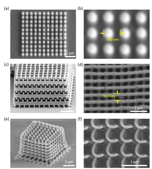
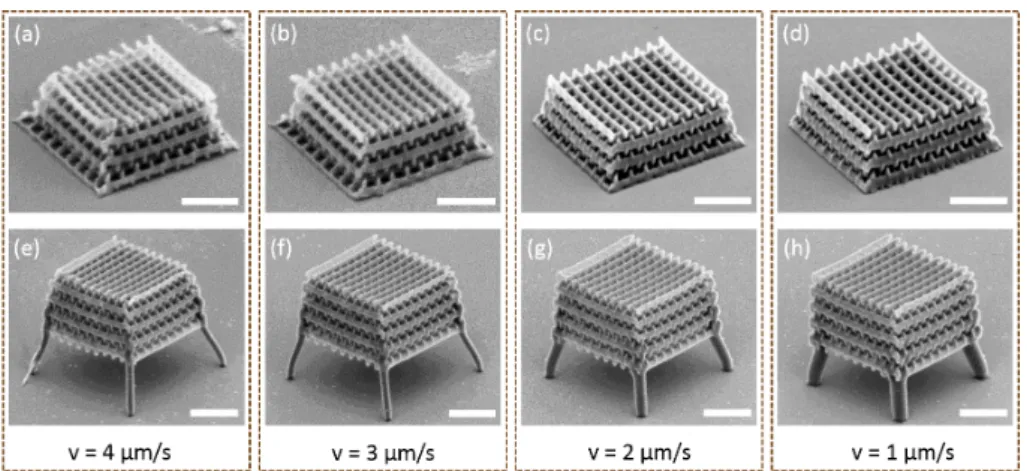
shows a 3D woodpile and a chiral structure created using LOPA DLW. The woodpile structure consists of 20 stacked layers, each layers consists of parallel rods with period a = 1.5 µm. The spiral structure was well created and is as good as those obtained by TPA DLW. The structures features are well separated, layer by layer, in horizontal and in vertical directions. The feature sizes are about 300 nm (horizontal) and 650 nm (vertical). The smallest feature size can reach 150 nm corresponding to the smallest lateral cross-section of rod. The best quality of the fabricated structure obtained when the line width of rods is about of the voxel standard size (lateral and axial cross-section size is about 220 nm and 680 nm, respectively. The corresponding aspect ratio (axial/lateral) is about 3.
Figure 2.5: (a-b) SEM images of a woodpile structure fabricated with the fol-lowing parameters: distance between rods = 1.5 µm; distance between layers = 0.7 µm; number of layers = 20; laser power P = 4 mW and scanning speed v = 1.5 µm/s. (c-d) SEM images of a chiral structure. Fabrication parameters: lattice constant a = 2 µm; distance between layers = 0.75 µm; number of layers = 28;
laser power P = 2.8 mW and scanning speed v = 1.34 µm/s.
However, there are still some existing drawbacks in structures fabricated by LOPA DLW, such as the energy accumulation effect, shrinkage effect, or high aspect
ratio [45]. In the next section, the thermal effect induced by a cw green laser in the LOPA-based DLW technique, which plays a role as a heat assistance for completing the crosslinking process of the photopolymerization of SU8, is investigated. This thermal effect will help overcome those drawbacks and significantly improve the quality of structures fabricated by LOPA DLW.
2.3 Theoretical model of optically induced local
thermal effect
In this section, by solving the heat equation, in which the laser was considered as a heat source, we explain the working principle of the optically induced thermal effect, also called local PEB.
First, the heat distribution in the laser-heated SU8 is calculated. When a laser beam propagates through an absorbing material, the temperature distribution in
the material can be derived from the equation of heat [73]:
ρCp
∂T
∂t = k∇
2T + S, (2.4)
where ρ is the mass density (kg.m−3), C
p is the heat capacity (J.kg−1.K−1), k is
the thermal conductivity (W.m−1.K−1), and the S(W.m−3) term is calculated as a
variation of light intensity along the propagation direction:
S = − ∂I(r, z)
∂z
! r
= µabs(1 − Rc)I(r, z) exp(−µabsz), (2.5)
where I(r,z) is the laser intensity, µabs is the absorption coefficient of the material,
and Rc is reflection coefficient. In our case, the light beam is focused into photoresist
by a high NA OL. The intensity distribution of the focused laser beam is calculated by:
I(r, z) = I(0, 0)IOPA, (2.6)
where r is the radial distance from the beam axis, z is the axial distance from the center of the focusing spot, I (0,0) is the peak intensity at the center of focusing
light in the focal region, which is rigorously calculated by using the vector Debye
method presented in Section2.2. By using finite element method with Matlab PDE
solver, Equation 2.4 was numerically solved to characterize the optically induced
heat profile. The optical intensity distribution at the focal region of a high NA OL for the xz−plane and corresponding induced temperature profile, obtained after 50
µs of exposure, are shown in Figure 2.6. Due to the absorption of the photoresist
and thanks to the optical intensity distribution (Figure 2.6(a)), a temperature
dis-tribution is produced at the focusing region (Figure 2.6(b)). It can be seen that
the normalized heat distribution is broader than the optical intensity distribution. However, looking closer at the peak of the temperature profile, we can see that there is only a tiny area where local temperature can surpass the effective temperature for PEB, i.e., 95°C where the complete crosslinking reaction takes place (see inset
of Figure 2.6(c)). The size of this area is even smaller than the full-width at half
maximum of the optical focusing spot, suggesting that a solidified structure made by optically induced thermal effect could be smaller than the diffraction limit, which usually limits the resolution of DLW technique.
The resolution of the DLW technique along the propagating direction of the laser beam (z-direction), i.e., the voxel aspect ratio, plays an important role in 3D
fabrication. As seen in Figure 2.6(a) which shows theoretical calculations of light
intensity distribution at the focal region, the longitudinal (z−axis ) size of the fo-cusing spot is about 3 times larger than the transverse size (x−axis). Meanwhile, the temperature distribution along the longitudinal direction (z−axis) is quite similar
to that of transverse direction (x−axis, or y−axis) as observed in Figure 2.6(b). It
means that the fabrication based on optically induced thermal effect could have an isotropic resolution for 3D structures.
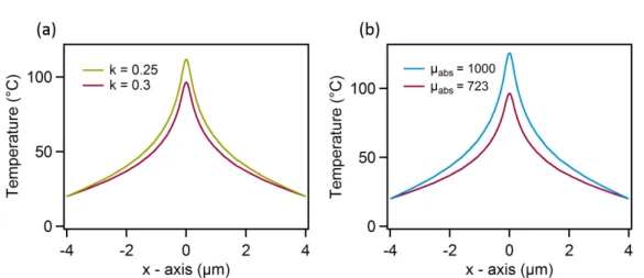
We note that the induced temperature is very sensitive to the exposure dose. Indeed, when a small area of material is strongly excited, the temporal thermal bal-ance is immediately broken due to the change of thermal constants. We also analysed thermal profiles for different values of thermal constants, assuming that we excite a small area of 200 nm-diameter to reach a temperature above 95°C. The thermal conductivity of the exposed part will be reduced from 0.3 to 0.25. The simulation results show that the thermal profile increases slightly and become sharper as shown
Figure 2.6: (a) Theoretical calculation of light intensity distribution at the fo-cal region of a high NA OL for xz–plane. (b) Corresponding heat distribution inside excited material for xz–plane. (c) Cross section of heat profile and light intensity distribution at the focal region for x–axis. The simulations were realized with following parameters: ρ = 1200 kg.m−3, Cp = 1200 J.kg−1.K−1, k = 0.3
W.m−1.K−1, R
c = 0, µabs = 723 m−1, S ≈ 1014 W.m−3 corresponding to a laser
power of 4 mW, and the initial temperature of material is 20°C.
(µabs) is also an essential parameter to define the transfer rate of the energy from the
focusing spot to the absorbing medium. Therefore, a minor modification of (µabs)
can lead to a significant change in the thermal response, i. e. induced temperature,
as shown in Figure 2.7(b). However, the absorption coefficient of SU8 at the
writ-ing wavelength (λ = 532 nm) does not significantly change for temperature range of 50°C–95°C. Therefore, by limiting the laser power or exposure time to keep the induced temperature in this range, the absorption coefficient is constant. Only, if we extend the exposure process, the temperature at the focusing spot will progressively increase and the cross-linked area will be expanded accordingly.
Solving the heat equation 2.1 with the depth taken into account, we calculated
Figure 2.7: (a) Comparison of temperature distributions obtained in two pos-sible cases: i) thermal conductivity is 0.3 for whole film (red), and ii) thermal conductivity is 0.25 at focusing center with a diameter of 200 nm and 0.3 on the remaining part (green). The simulations were realized for only x-axis with follow-ing parameters: (ρ = 1200 kg.m−3, Cp = 1200 J.kg−1.K−1, µabs = 723 m−1, the
laser power of 4 mW. (b) Comparison of temperature distributions in two cases: i) absorption coefficient is constant (µabs = 723 m−1) for whole region (red), and ii) absorption coefficient at focusing center with a diameter of 100 nm is µabs = 1000
m−1 and that of the remaining part is µabs = 723 m−1 (blue).
Figure 2.8: (a) Simulation result of local peak temperature at different values of focusing depth with different laser powers. (b) The evolution of optically induced
temperature as a function of exposure time at the laser power of 5 mW.
532 nm (µabs = 723 m−1), light can be tightly focused inside the material while the
intensity does not decrease much, resulting in a photo induced thermal effect with high temperature even at large penetration depth. This is evident in the calculation
result shown in Figure2.8(a), which presents the local peak temperature as a
goes inside the material, the lower the temperature is due to the decrease of the light intensity. However, the induced temperature changes only slightly, for example, with
a laser power of 5 mW (intensity of 0.11 W µm−2), the temperature decreases by
only 5°C (from 99°C to 94°C) when the focusing spot goes from the interface to a depth of 75 µm. The higher the used intensity is, the deeper the focusing spot can go inside the material with the peak temperature remaining above the required temperature for PEB. Thus, it is possible to fabricate 3D structures using LOPA DLW with local PEB.
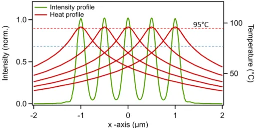
Figure 2.9: Intensity distribution (green curve, corresponds to the left axis) and temperature distributions (red curves, correspond to the right axis) of multiple exposures. The red dotted line (corresponds to the right axis) represents the global temperature by the hot plate; The blue dotted line represents the iso-intensity.
More importantly, LOPA DLW with local PEB can help overcome some
draw-backs existing in traditional LOPA DLW. Figure2.9illustrates the working principle
of traditional PEB on a hot plate (green curves) and optically induced local PEB (red curves). In the first case, heat is broadly provided, thus the fabricated structure (voxel size and shape) depends critically on the exposure dose. When the exposures are made too close, the energy will be accumulated, leading to the effect that the central voxel possesses a largest size (due to the most accumulated energy) and the voxels sizes gradually reduce from the center to the edge. Solidification of structure resulting from photothermal process differs from that of photochemical process in term of accumulation. In the second case, although the energy is still accumulated, the voxel size is determined by the local PEB, which resulting from the optically
induced heat distribution. The red curves in Figure 2.9 show the temperature pro-file generated by a focused laser spot (laser power of 4 mW, or intensity of 0.088
W µm−2) inside the exposed area. With moderate excitation power, the induced
temperature is just enough to complete the PEB step and does not damage the fab-ricated structure. Furthermore, the induced temperature is not only localized but also temporal, i.e., during the exposure time only. In our DLW method employing a cw laser, we found theoretically that the induced temperature at the focusing spot rises up quickly as a function of exposure time and reaches a stable temperature
(beyond 100◦C) after several 10 µs, depending on the exposure power (see Figure
2.8(b)) and remains at that temperature during the exposure time, which is in
be-tween 10 ms and 1000 ms. This time scale is consistent with previous heat models on
other polymer materials [74]. Figure 2.9 shows the integrated light intensity profile
resulting from multiple exposures at a 500 nm period (green curve) and heat profiles generated temporally during each exposure time. Thus, even when the light energy is accumulated in case of LOPA-based DLW, the localized and temporal temperature profile is the same for every exposure without accumulation, resulting in the uniform solid voxels array. We note that, using a femtosecond laser, the induced temperature increases quickly to one million degrees but also decreases quickly to room
temper-ature [75] (the heating time is the same as the femtosecond pulse duration), which
is not suitable to solidify the photoresist. Therefore, DLW using a femtosecond laser
does not induce such thermal effect, except the result reported in reference [65],
where the femtosecond pulse excitation induced high temperature that plays a role as a blackbody source emitting IR light, which enhances the polymerization of SU8 during the exposure by direct absorption. We also note that the voxel size increases as the exposure time rises since the voxel size depends on both the exposure dose (ex-posure time) and the PEB time. It is also worth noting that, when using traditional PEB, the exposure step and PEB step are separated, which means the photoacids have sufficient time to diffuse into exposed region, whose overlap is then fixed by PEB, leading to non-uniform structures. On the contrary, optically induced PEB occurs simultaneously with optical exposure, providing a highly localized immediate fixing in a small region inside the focusing spot which is not affected by the dif-fusion. In summary, we have demonstrated theoretically the working mechanism of the optically induced thermal effect by solving a heat equation. The results prove that it is possible to apply this effect to LOPA-based DLW technique to create 1D,
2D and 3D microstructures, and to optimize the quality of fabricated structures. In the next section, we will implement the experiments to confirm the theoretical calculation results.
2.4 LOPA-based DLW by local PEB
2.4.1 LOPA-based DLW system
The LOPA technique can be used for all 3D applications, including 3D imaging
and 3D fabrication. As mentioned in section 2.1, two conditions are required: a
photoresist that presents an ultralow absorption at the wavelength of the excitation laser, and a highly focusing confocal laser scanning (CLSM) system. For the first condition, SU8, a commercial photoresist, is an ideal candidate, thanks to its ultralow
absorption in the visible range, in particular at 532 nm (Figure 2.10), which is the
wavelength of a very popular and low cost solid state frequency-doubled neodymium laser. By using a high NA oil-immersion OL of NA = 1.3 to focus a laser beam into the photoresist, the second condition is then satisfied.
Figure 2.10: Absorption spectrum of SU8 photoresist. The color bars indicate three cases: OPA (purple bar), LOPA (green bar), and TPA (red bar). To
demon-strate LOPA DLW, a laser operating at 532 nm is used.
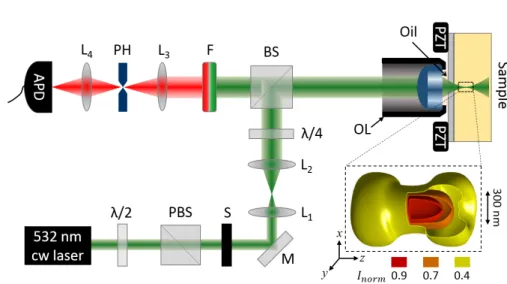
is used. In order to adjust the power of the laser beam to the sample, we used a half-wave plate (λ/2) and a polarizer (PBS). By rotating the half-wave plate, the power of the laser beam can be precisely modified. A powermeter (not shown in the figure) is used to measure the power of the laser beam. The laser beam is directed and collimated by a set of lenses and mirrors. In order to realize mapping or fabrication, samples are mounted on a 3D piezoelectric actuator stage (PZT), which is controlled by a LabVIEW program. A quarter-wave plate (λ/4) placed in front of the OL allows one to transform the beam of linear polarization to circular polarization before it enters the OL. The laser beam is strongly focused to the sample via an OL with high NA (1.3). The time of exposure of the sample to the laser beam is determined using an electronic shutter, which is also controlled by a LabVIEW program. The fluorescence signal emitted by the samples is collected by the same OL, filtered by a 580 nm long-pass filter (to cut off the excitation wavelength of 532 nm), and detected by an avalanche photodiode (APD). The inset of Figure
2.11 shows the simulation result of the light intensity distribution at the focusing
region of the OL. The maximal intensity was normalized and three iso-intensities are shown. This suggests the evolution of the structure size and shape, which is linearly dependent on the exposure doses (excitation power and exposure time) and can be
controlled by applying an appropriate dose [45]. By scanning the focusing spot, we
can obtain desired multi-dimensional structures, which are similar to those realized by the commercial TPA-based DLW.
Below we describe in detail some optical components of the setup, which are used in all experiments of the thesis.
Laser source: In this work we used a cw laser operating at 532 nm for fabrication
of PSs in SU8 photoresist. A pulsed laser operating at 1064 nm was used for sec-ond harmonic generation (SHG) measurement of KTP NPs (details in Chapter 5). Besides, cw 532 nm laser source was used for all system characterizations (confocal system, data acquisition calibration, etc.) using a single gold nanoparticle (Au NP). • Pulsed laser (JDSU): 1064 nm wavelength; maximum averaged power: 300
Figure 2.11: Experimental setup of the LOPA-based DLW technique. PZT: piezoelectric translator, OL: oil immersion microscope objective, λ/4: quarter-wave plate, λ/2: half-quarter-wave plate, BS: beam splitter, PBS: polarizing beam splitter, M: mirror, S: electronic shutter, L1−4: lenses, PH: pinhole, F: 580 nm long-pass filter, APD: avalanche photodiode. Inset: Simulation result of intensity distribu-tion at the focus region of a high NA OL. Three surfaces correspond to three isointensities, 0.4; 0.7; and 0.9, respectively. The optical axis of the OL is z-axis.
• Continuous wave laser (Oxxius): frequency-doubled Nd-YAG laser, 532 nm wavelength, maximum power: 300 mW, coherence length: 300 m; pointing sta-bility: 0.005 mrad/C.
Translation system: In order to precisely translate the sample relatively to the
focusing spot during fabrication, DLW requires a high-resolution piezo-based trans-lation PZT system. In our experimental setup, a high-precision nanopositioning system for up to six degrees of freedom is used (P365 PIMars Nanopositioning Stage -Physik Instrumente). This piezo-based translation system offers a large travel ranges
of 300 × 300 × 300 (µm3) and very high precision. According to the company
spec-ification, this device shows a resolution of 1 nm when operating in open-loop and 2 nm in close-loop. The stability for an accuracy of about 10 nm can maintain within a long period of up to 5 hours. However, the precision and the stability is very sensitive to the mechanical vibration and ambiant temperature. We keep the PZT system remote from mechanical noise source and the room temperature was maintained within 20-25°C.