Prepared for submission to JINST
FATALIC: A novel CMOS front-end readout ASIC for the
ATLAS Tile Calorimeter
S. Angelidakis1W.M. Barbe R. Bonnefoy H. Chanal C. Fayard R. Madar1S. Manen
M.-L. Mercier E. Nibigira D. Pallin N. Pillet L. Royer A. Soulier R. Vandaële F. Vazeille
Laboratoire de Physique de Clermont-Ferrand, CNRS/IN2P3, Université Clermont Auvergne, 4 avenue Blaise Pascal, Aubière, France
E-mail: Stylianos.Angelidakis@cern.ch,romain.madar@clermont.in2p3.fr
Abstract: The present article introduces a novel ASIC architecture, designed in the context
of the ATLAS Tile Calorimeter upgrade program for the High-Luminosity phase of the Large Hadron Collider at CERN. The architecture is based on radiation-tolerant 130 nm Complementary Metal-Oxide-Semiconductor technology, embedding both analog and digital processing of detector signals. A detailed description of the ASIC is given in terms of motivation, design characteristics, simulated and measured performance. Experimental studies, based on 24 prototype chips under real particle beam conditions are also presented in order to demonstrate the potential of the architecture as a reliable front-end readout electronic solution.
Keywords: Front-end electronics for detector readout, Calorimeter methods
1Corresponding author.
Contents
1 Introduction 2
2 The ATLAS Tile Calorimeter 2
3 Upgrade of the Tile readout 4
4 The FATALIC Architecture 5
4.1 Fast channels 6
4.2 Slow channel 7
4.3 Outputs 7
5 Development of the integrated circuit 8
5.1 Current conveyor system 8
5.2 Signal shaping 9 5.3 Signal digitisation 9 5.4 Digital block 12 5.5 Floorplan 12 5.6 Design verification 13 6 Associated cards 14 6.1 All-in-one card 14 6.2 Mainboard 15
7 Simulation and performance 15
7.1 Noise measurements 17
7.2 Linearity measurements 18
7.3 Performance of the analog and digital block 18
7.4 Radiation tolerance 21
8 Energy reconstruction 24
8.1 Selection of digitised samples 24
8.2 Simulation of experimental effects 24
8.3 Two-gain scenario 26
9 Performance with particle beams 27
9.1 Inter-calibration of readout channels 27
9.2 Measurement of particle deposits 27
1 Introduction
The Large Hadron Collider (LHC) [1] at CERN is scheduled to undergo a decisive upgrade [2], which will extend its physics potential well beyond the initial design goal [3,4]. The first phase (Phase-I) of the upgrade will take place during the long technical shutdown of the LHC, in 2019-2020, to improve the injector and the collider collimation system. In the second phase (Phase-II), scheduled for 2024-2026, the LHC will be further enhanced with new technologies, including 11-12 T triplet magnets and compact crab cavities with ultra-precise phase control. The final High Luminosity LHC (HL-LHC) is expected to begin operation in 2026, delivering proton-proton (pp) collisions with a maximum instantaneous luminosity of 7.5 × 1034cm−2s−1(7.5 times higher than the initial design). In terms of total integrated luminosity, a goal of 3000-4000 fb−1is defined.
In order to perform in the high intensity radiation environment of the HL-LHC, where up to 200 inelastic pp collisions (pile-up events) per 25 ns bunch crossing are expected, the ATLAS detector [5] is scheduled for upgrade of its sub-detector systems as well as the Trigger and Data AcQuisition (TDAQ) strategies [6]. In this context, the Phase-II upgrade program foresees the replacement of the readout electronics of the Tile Calorimeter (TileCal) [7,8], the central hadronic calorimeter of ATLAS, with new architectures that will be able to deliver reliable measurements during the HL-LHC operation. Among the different designs proposed and evaluated for the Front-End (FE) readout electronics, the Laboratoire de Physique de Clermont-Ferrand (LPC) presented the solution of an ASIC that embeds both the analog processing and digitisation of the detector signal, the Front-end ATlAs tiLe Integrated Circuit (FATALIC). The following sections intend to provide a detailed description of the FATALIC motivation and design, and present simulation and experimental measurements to demonstrate its potential as a FE readout system.
2 The ATLAS Tile Calorimeter
TileCal is a sampling calorimeter, constructed of steel plates as absorber and scintillating tiles as active medium, and it is important for the measurement of jet- and missing-energy, jet substructure, electron isolation and triggering (including muon information). The position of TileCal in the
ATLAS calorimeter complex can be seen in figure1a. It is divided into four cylinders, two of
which form the central Long-Barrel (LB) while the other two constitute Extended-Barrel (EB) partitions, covering the pseudorapidity1range |η| < 1.7. Each Tile cylinder is made of 64 wedge
modules (figure1b) in the azimuthal coordinate. The Photo-Multiplier Tubes (PMTs) with the
associated FE readout electronics and high voltage distribution cards are inserted at the outer radius of each module, hosted by a train of two 1.4 m long “drawers” which form a “super-drawer” (one super-drawer can host up to 48 PMTs).
The scintillation light is collected from the two opposite sides of the tiles by wavelength-shifting (WLS) fibres, which are bundled, to define readout cells, and coupled to a pair of PMTs. The current pulse induced at the PMT anodes, with a typical width of 10 ns, is therefore proportional to the
1ATLAS uses a right-handed coordinate system, centered at the nominal interaction point. The x-axis points towards the center of the LHC ring, the y-axis points upwards and the z-axis points along the beampipe. Cylindrical coordinates (r,φ) are used in the transverse plane, φ being the azimuthal angle around the z-axis. The pseudorapidity is defined in
(a)
Photomultiplier
Wave-length shifting fiber Scintillator Steel Source tubes (b) 500 1000 1500 mm 0 A3 A4 A5 A6 A7 A8 A9 A10 A1 A2 BC1 BC2 BC3 BC4 BC5 BC6 BC7 BC8 D0 D1 D2 D3
A13 A14 A15 A16
B9 B12 B14 B15 D5 D6 D4 C10 0,7 1,0 1,1 1,3 1,4 1,5 1,6 B11 B13 A12 E4 E3 E2 E1 beam axis 0,1 0,2 0,3 0,4 0,5 0,6 0,8 0,9 1,2 2280 mm 3865 mm η=0,0
~
~
LB EB (c)Figure 1: (a) The calorimeter system of ATLAS. (b) Schematic of a wedge module. (c) Tile cell mapping.
energy deposited in the respective cell and is fed to the FE electronics to be amplified, shaped and digitised at the 40 MHz LHC clock rate. This arrangement of the readout employs a total of 9852 PMTs and segments TileCal into three radial layers (figure1c), classified as "A", "BC" and "D", with depth 1.5, 4.1, and 1.8 interaction lengths, respectively, at η= 0. Each A-BC-D cell grouping in the same η-direction forms a projective tower currently used for the fast trigger. Additional scintillators (E cells) are installed in the region between the LB and the EB, mainly to measure energy escaping the electromagnetic calorimeter, while at higher |η|, Minimum Bias Trigger Scintillators (MBTS) are used to monitor minimum-bias event rates. The E and MBTS scintillators have been used to monitor the luminosity during van der Meer scans2 [9] and are also useful in electron identification.
To ensure stable measurements, TileCal incorporates three calibration systems. A Charge Injection System (CIS) [10] is used to monitor the response of the FE electronics to known injected charge, but also to derive the conversion factors between the electronic responses and the input charge. Next, the Cesium (Cs) system [11, 12] uses a radioactive 137Cs γ-source, hydraulically circulated through a system of tubes that traverses every row of scintillating tiles. The illumination of the tiles with 0.662 MeV γ produces a uniform, low current signal at the PMT anodes that allows inter-calibration of the detection chains (scintillators, WLS fibres, PMTs, FE electronics). After initial adjustment of the PMT gains, the Cs system is used to measure the small variations among the read-out responses, which are used to derive the necessary calibration coefficients with respect to a unique reference value. Lastly, the laser system [13] injects light pulses to the PMTs for frequent monitoring of the gains between Cs scans.
3 Upgrade of the Tile readout
In the current Tile readout scheme, the 256 super-drawers are interfaced to back-end Read-Out Drivers (RODs) through 256 optical links (plus another 256 links for redundancy) with a bandwidth of 800 Mbps per link. Each super-drawer stores the digitised samples from the read-out Tile cells in pipeline memories, while analog trigger signals, corresponding to each Tile tower, are transmitted to the off-detector trigger pre-processor. These trigger signals are formed by summation of the PMT outputs, in dedicated analog boards, with rough adjustment in time but without calibration to account for gain variations. Upon trigger acceptance, the data of each super-drawer are forwarded to the RODs.
For the HL-LHC, the TDAQ strategy [8] foresees a fully digital calorimeter trigger with higher granularity and precision. Each super-drawer is replaced by four independent mini-drawers, with half the length of the current drawers to allow easier access to the electronics and improve the reliability of the cooling circuits. At the 40 MHz rate, each mini-drawer transmits the entire set of digitised data to an off-detector PreProcessor (PPr) [14] over two 9.6 Gbps optical links (the full readout scheme employs 2048 optical links plus another 2048 links for redundancy). The PPr stores the data in pipeline memories and, in parallel, transmits calibrated trigger primitives (energy measured in grouped or individual Tile cells) to the trigger system. Upon receipt of a trigger acceptance signal, the reconstructed energy, the time and a quality factor for each Tile cell are forwarded to the data network for event aggregation and storage.
In the new Tile readout system, the present reliable but outdated Tile FE electronics will be replaced by a new architecture that will be able to endure the harsh radiation conditions anticipated
at the HL-LHC (up to 50 krad Total Ionising Dose, as presented in Section7.4) and handle the
expected dynamic range of the input signal. The lowest expected signal from physics events is defined by the minimum ionisation Landau peak of muons traversing an A cell (smallest Tile cell) at normal incidence, with a most probable value of 350 MeV [15]. Considering the typical electromagnetic (EM) scale constant of 1.05 pC/GeV and the e/µ response ratio of 0.91, the respective charge delivered by a single PMT is approximately 200 fC. On the other hand, the largest expected signal is that of energetic jets, depositing up to 1.3 TeV in EM scale (1.5 TeV in hadronic
beams transversely across each other. Being responsible for luminosity measurements in ATLAS, TileCal must be able to measure very low Minimum Bias event rates.
scale) in a single Tile cell. To cover this range, the maximum charge requirement for one readout channel is set to 800 pC. There is however interest in extending the range up to 1.2 nC to be able to measure higher energy jets, expected in rare and possibly new physics events. In addition to the processing of physics signals, each FE electronic card must include a separate channel for large time-constant integration of low amplitude currents. This channel is needed for calibration scans using the Cs system (50 nA − 100 nA) but also for the monitoring of minimum-bias event rates and the instantaneous luminosity (20 pA − 10 µA).
4 The FATALIC Architecture
FATALIC is an ASIC, based on 130 nm GlobalFoundries (GF) Complementary Metal-Oxide-Semiconductor (CMOS) technology, designed to replace the current, discrete FE readout elec-tronics of the TileCal. The proposal of an ASIC, embedding both analog signal processing and digitisation, is motivated by its significant advantages in terms of simplicity, radiation tolerance, power consumption and production cost for a large number of chips. On the other hand, since the operating low voltage (1.6 V) is dictated by the technology, FATALIC must rely on a current-driven, rather than a voltage-driven architecture to handle the large input dynamic range. Hence, an input stage employing current conveyors is implemented to adjust the impedance and distribute the signal
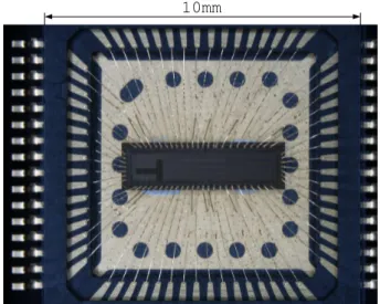
to the different channels. Figure2 shows a FATALIC chip, wire-bonded inside a 64-pin LQFP
package.
The specifications of FATALIC are listed in table1, while a block diagram summarising the architecture is given in figure3. In order to handle the large input range (up to 1.2 nC), FATALIC provides three fast channels to process the PMT signal at the 40 MHz LHC clock rate, with relative amplification ×1 (low gain), ×8 (medium gain) and ×64 (high gain). This three-gain scheme is chosen, instead of using two gains, in order to improve the energy resolution (at the Tile cell level) across the input range, as shown by the related study in Section8.3. In parallel, the signal is routed to an additional, slow channel for integration over a large (100 µs) time constant.
10mm
ADC 12b 40 MS/s ADC 12b 40 MS/s ADC 12b 40 MS/s 24 High-Gain fast channel
Gain flag IPMT FATALIC ANALOG CORE Current Conveyor shaper Current Conveyor shaper Current Conveyor shaper Medium-Gain fast channel
Low-Gain fast channel
ADC 12b 1 MS/s Current Conveyor Slow Integrator Slow-channel DIGITAL BLOCK 24 24 24 DIGITAL CONVERTERS ADC bits processing + Gain Selection + Data Output multiplexing Fast channels Data output (12b@80Mbps) Slow channel data output (1b@10Mbps) Low-Gain selection
Figure 3: Block diagram of FATALIC.
Technology 130 nm CMOS GF
Number of channels per ASIC 1
Polarity negative
Fast channel dynamic range in charge 25 fC - 1.2 nC
Fast channel dynamic range in current peak 1.25 µA - 60 mA
Rise time of the current peak 4 ns
Fall time of the current peak 36 ns
Fast channel noise (rms) <12.5 fC
Slow channel dynamic range in average current 0.5 nA - 1 µA
Slow channel Noise (rms) 0.25 nA
Power consumption ∼200 mW
Power supply 1.6 V
Output 12-bit words
Table 1: Specifications of FATALIC.
4.1 Fast channels
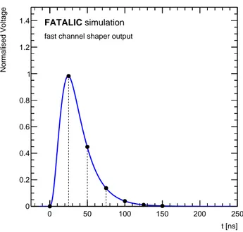
In the fast channels the signal is read by three current conveyors with different input impedances, which define the respective gain ratios. Current integration and current-to-voltage conversion follow at the transimpedance-shaping stage by three identical shapers, composed by a differential amplifier with RC feedback loop. A 25 ns time constant is used to produce an asymmetric output pulse with 25 ns peaking time, as shown in figure4. The digitisation is carried out in the ASIC, by 12-bit 40 MS/s Analog-to-Digital Converters (ADCs), to avoid degradation of the signal during transmission to an external converter. This establishes an effective 18-bit dynamic range and defines the range of each channel: 25 fC-20 pC (high gain), 200 fC-164 pC (medium gain) and 1.6 pC-1.3 nC (low gain).
0 50 100 150 200 250 t [ns] 0 0.2 0.4 0.6 0.8 1 1.2 1.4 Normalised Voltage simulation FATALIC
fast channel shaper output
Figure 4: Typical analog output pulse (simulation) from the fast channel shapers. At the 40 MHz clock rate, the 2ndsample coincides with the pulse peak.
4.2 Slow channel
The slow channel is designed to integrate low amplitude currents in the range from 0.5 nA to 1 µA with minimum contamination from1/f noise, induced by the input stage. A current conveyor with
low input impedance is therefore used to drive approximately 87% of the PMT signal to the slow channel, while current integration and current-to-voltage conversion are carried out by a differential amplifier with large time-constant (100 µs) RC feedback. The integrated signal is then sampled by a 12-bit 833 kS/s ADC. Finally, to minimise the contamination from white noise in the measurement of such low amplitude currents, the data are obtained after averaging over a time interval of 10 ms, as described in Section6.
4.3 Outputs
The 12-bit fast channel samples are read-out from 12 respective output pins. In order to comply with the bandwidth of the uplink to the back-end electronics (see Section6), FATALIC is restricted to provide the data of only two of the three channels; the 12-bit data of the medium-gain channel are always delivered upon the rising edge of the 40 MHz clock, while the data of either the low-or the high-gain channel (alternative gain) are delivered upon the falling edge. The selection of the alternative gain is made by the embedded digital block, depending on the saturation of the most sensitive channel (dynamic gain switch), and is declared by an output flag. The dynamic gain switch can however be forced to provide only low gain readout by a dedicated input bit. On the other hand, slow channel data are delivered serially, at 10 Mbps (833 kHz for the 12 bits), through a single readout pin.
5 Development of the integrated circuit
5.1 Current conveyor system
The current conveyor system, schematically depicted in figure5, consists of one input stage and four output stages, which provide differential signal to each of the FATALIC channels. At the input stage, a current mirror sets the biasing current to the nominal value of 0.5 mA. The PMT signal
is read at the source of four common-gate NMOS3 with the same length (L) but with different
widths: Wfast/1 (high gain), Wfast/8 (medium gain), Wfast/64 (low gain) and Wslow= 8 Wfast(slow
channel). A PMOS4 current mirror is then used to replicate the current from the drain of each
NMOS onto the respective output stage, while a replica of the input stage (dummy) is implemented to return just the biasing current to be subtracted from the final output.
In terms of noise, the performance of such current-conveyor is modest compared to a charge preamplifier, but well adequate, given the large dynamic range of input stage. The input impedance is kept below 70 Ω for the entire input range, as presented in figure6. Finally, to account for the open-loop configuration of the input stage, which induces large dispersion among the pedestal values, a tuning system with a Digital-to-Analog Converter (DAC) is also added to the above design.
Wfa
st
/64
IPMT
Wslow Wfast Wfast/8 Wfast/64
Ibia s_ s Ibia s_ s IDAC DUMMY INPUT STAGE Ibia s_ f Ibia s_ f Ibia s_ f /8 Ibia s_ f /8 Ibia s_ f /64 Ibia s_ f /64 Islow+ Wfa st /8 Wfa st Wsl o w Islow
-INPUT STAGE OUTPUT STAGE
Islow Ifast
/8
Ifast
/64
Ifast
Figure 5: The current conveyor system, consisting of the input stage, the four output stages and a replica (dummy) of the input stage in order to subtract the biasing current from the differential output.
3Negative channel Metal Oxide Semiconductor 4Positive channel Metal Oxide Semiconductor
4 − 10 10−3 10−2 10−1 1 Injected Charge [nC] 0 20 40 60 80 100 120 140 160 180 200 [Ohm]in Z simulation FATALIC Ibias = 0.5 mA = 0.2 mA bias I
Figure 6: Input impedance as a function of the input charge for the nominal biasing current, Ibias = 0.5 mA, and for a test value of Ibias= 0.2 mA.
5.2 Signal shaping
The shaper (figure7a) is a differential amplifier with RC feedback loop, with a time constant of 25 ns (R= 5 kΩ, C = 5 pF) in the fast channels and 100 µs (R = 500 kΩ, C = 200 pF) in the slow channel. The amplifier is based on a folded-cascode boosted architecture, depicted in figure7b, with two differential input pairs, one NMOS and one PMOS, and Common Mode FeedBack (CMFB) to control the output common mode. Its open-loop characteristics are listed in table2.
Open-loop gain 84 dB -3db bandwidth 38 kHz Unity-gain bandwidth 650 MHz Slew rate 220 V/µs Phase margin 85◦ Supply voltage 1.6 V Consumption 2.3 mA
Table 2: Open-loop characteristics of the shaper with the ADC input capacitive load of 1.6 pF.
5.3 Signal digitisation
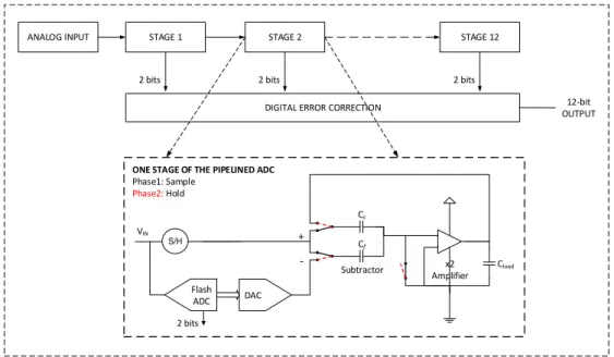
The shaper output is sampled by three 12-bit 40 MS/s ADCs in the fast channels and one 12-bit 833 kS/s ADC in the slow channel. The ADC design by LPC is based on the pipeline architecture
+ + -IIN+ V OUT -VOUT+ IIN -(a) IN+ OUT CMFB IN-IN+ (b)
Figure 7: (a) Schematic of the shaper, consisting of a differential amplifier with RC feedback loop. (b) Architecture of the differential amplifier.
with 1.5-bit-per-stage resolution. Among the various efficient ADC architectures developed and improved over the last ten years, the pipelined ADC has been adapted for high resolution, speed and dynamic range with relatively low power consumption and low component count. In CMOS technologies, resolutions in the range of 10-14 bits with a sampling frequency up to 100 MS/s are typically achieved with power consumption lower than 100 mW.
Figure8 presents the block diagram of the pipelined ADC, with two output bits per stage,
displaying the architecture of one of the stages. Each stage receives a differential input voltage, in the range ±500 mV, which is read by a sample-and-hold (S/H) and a 2-bit flash ADC. The flash ADC compares the input to two threshold voltages (±125 mV) and outputs a 2-bit word, while a DAC and a residue amplifier provide the input to the next stage, as presented in table3. Although a
2-bit word is delivered, the effective resolution is 1.5-bit since the combination 11 is avoided. This bit redundancy limits the degradation of the Integral Non-Linearity5(INL) due to variations of the residue amplifier gain or the comparator offsets (the INL is unaffected by variations of the offset voltage for up to ±12.5% of the full-scale input voltage). The complete architecture includes 12 cascading stages and is followed by the digital correction block (see Section5.4), which delivers the final digital code. The estimated power consumption of the ADC is 48 mW.
Vini [b2b1] DAC Vini+1
Vref/4 - Vref [10] Vref/2 2Vini − Vref
−Vref/4 - Vref/4 [01] 0 2Vini
−Vref - −Vref/4 [00] −Vref/2 2Vini + Vref
Table 3: Each stage i of the pipeline converts the input voltage Vini, in the dynamic range ±Vref, into
a 2-bit word [b2b1] and feeds the amplified residual Vini+1= 2(Vini − DAC) to the next stage.
The comparator. The architecture of the comparator is presented in figure9. The
transcon-ductance input stage is fully differential, comparing the differential input signal to the differential threshold voltage, while isolating the input from kick-back noise, induced by the switching of the subsequent latched stage. The latched stage performs the comparison when the switch-transistors are OFF and a reset when they are ON. The state of the comparator, when it is latched, is memorised
STAGE 1 STAGE 2 STAGE 12
DIGITAL ERROR CORRECTION ANALOG INPUT
12-bit OUTPUT
2 bits 2 bits 2 bits
x2 Amplifier Cs Cf Cload VIN Flash ADC DAC
ONE STAGE OF THE PIPELINED ADC
Phase1: Sample Phase2: Hold S/H 2 bits Subtractor -+
Figure 8: Block diagram of the 12-bit pipelined ADC with two output bits per stage.
5The INL is defined as the deviation, in Least-Significant-Bits (LSBs), of the output code from the ideal transfer-function.
thanks to the bistable third stage. Lastly, two NOT gates perform the final digital shaping of the output signal. The main characteristics of the comparator are given in table4.
The DAC. The DAC employs a set of switches, controlled by the comparators, to select the
differential reference voltage to be applied on the feedback capacitor of the residue amplifier. Given the ±500 mV input dynamic range, the reference voltages are set to ±250 mV.
Clocking frequency 40 MHz
Sensitivity 50 µV
Power supply 1.6 V
Power consumption 2.1 mW
Table 4: Characteristics of the comparator.
The gain-2 residue amplifier. The residue amplifier, displayed in figure8, is a differential
ampli-fier with capacitive feedback. Capacitive, rather than resistive feedback is used for better component matching, which is crucial for the accuracy of the amplification and, therefore, the linearity of the ADC. A capacitance of 800 fF is sufficient to minimise both the thermal noise (kT /C) and the
component mismatch (∼1/√C). On the other hand, the design requires a small die surface and
low supply current for dynamic performance. To match both the sampling (CS) and feedback (CF)
capacitance to 800 fF, with an accuracy better than 0.1%, an array of four 1600 fF MIM capacitor unit cells is drawn in common-centroid layout, while dummy switches are added to counterbalance parasitic capacitors introduced by the reset switches. Lastly, the timing sequence, controlling the sample, hold/amplification and reset phases of each stage, has been carefully defined to prevent charge disruption.
5.4 Digital block
Each ADC delivers twelve 2-bit words at the 40 MHz clock rate. The result of the complete conver-sion is therefore a 24-bit word with 12 redundant bits. The digital block (figure10) synchronises the outputs using shift registers to compensate for the delay due to the position of each stage in the pipeline. The total latency of this process is equal to eight clock cycles (200 ns) and it is fixed for every power cycle. Digital summation (with carry-save) of the most-significant bit of each stage with the least-significant bit of the previous stage is then performed to the final 12-bit code every 25 ns for the fast channels and 1.2 µs) for the slow channel. The second function of the digital block is to select the alternative gain output between the high-gain and the low-gain channel data (see Section4.3). This selection is made according to the output of the low-gain channel; if it is equal or higher (lower) than 600 ADC counts, then the low-gain (high-gain) channel data are delivered.
5.5 Floorplan
The floorplan of FATALIC (figure11) is optimised for minimum surface, while preserving signal integrity. Two main regions are distinguished; the region hosting the input stage and the shapers (analog block), and the region hosting the ADCs and the digital block. The two regions are isolated
VREF VIN
VOUT
STAGE 1 STAGE 2 STAGE 3
Figure 9: Architecture of the comparator (single-ended representation for simplicity).
Digital delay & Summation if 1 if 0 if 1 if 0 Digital delay & Summation ADC (g8) ADC (g1) Digital delay & Summation ADC (g64)
<
64 +/- offset Digital delay & Summation ADC (slow) Gain flagADC OUT (fast)
1 if true
Low-gain selection ( 0 for low gain)
NAND 1 if true Clk_40MHz 12 12 12 Divider (833kHz)
Serializer ADC OUT (slow)
12 12 24 24 24 24 1 12
Figure 10: Architecture of the digital block.
by a high impedance (BFMOAT) layer to reduce the coupling. The analog power and reference voltage rails are also decoupled by embedded large capacitors. The total surface of the chip measures 7.5 mm2, while the core area is limited to 2.3 mm2.
5.6 Design verification
All standard verification checks have been performed for the design of FATALIC. The analog part was tested with Monte Carlo simulations, using the Virtuoso Analog Design Environment by
Figure 11: The floorplan of FATALIC. Two main regions are distinguished; the region hosting the analog blocks (left) and the region hosting the ADCs and the digital block.
Cadence. The yield with process and mismatch is evaluated to 90%, while the offset of the input stage, which is an open loop configuration, is tunable to maintain a high yield and was assessed with mismatch simulations. Corners simulations did not highlight sensitivity of the ASIC to the temperature or the power supply. For the digital part of the ASIC, simulations were performed with SOC Encounter, while for the full ASIC, mixed-mode simulations were performed with the Virtuoso Analog Mixed-Signal (AMS) Designer. Finally, the good performance of the ASIC is confirmed with all of the 24 prototype chips that were produced.
6 Associated cards
Figure12displays a fully equipped mini-drawer, hosting 12 PMTs, 12 “All-in-One” cards, each of which contains one FATALIC chip and the dedicated CIS, and the Mainboard, which controls the All-in-One cards and transmits the data to the Daughterboard. Both the All-in-One cards and the Mainboard have been designed by LPC for the purposes of FATALIC. The Daughterboard, also shown in figure12, is the on-detector interface to the back-end electronics. It is divided into two independent sides, each of which establishes a 9.6 Gb/s uplink to deliver the data of six readout channels to the off-detector PPr, while a 4.8 Gb/s downlink is used to transmit the LHC clock as well as control and configuration commands.
6.1 All-in-one card
The All-in-One card contains FATALIC and the CIS. It is based on a 6-layer Printed Circuit Board (PCB) with dimensions 7.0 cm × 4.7 cm. On one side, a 7-pin connector attaches the card to the high-voltage divider, at the basis of the PMT, while on the opposite side a 40-conductor ribbon cable establishes communication with the Mainboard. Finally, nine on-board potentiometers adjust the low voltage supply and the pedestal for each channel.
A schematic diagram of the CIS is given in figure13. The charge injection is driven by
a 12-bit DAC with maximum output 4.095 Volts. The DAC charges one of the three available capacitors, 5.6 pF, 39 pF or 330 pF, for the scanning of the high-, medium- or low-gain dynamic range, respectively. The connected capacitance is defined through analog switches, controlled by two timing signals from the Mainboard. The same timing signals control the charge/discharge
FATALIC on
All-In-One cards Mainboard Daughterboard
PMTi Off-detector electronics
x 12
Figure 12: Schematic view of the readout chain. Left: the All-In-One card supporting FATALIC. Right: a fully equipped mini-drawer housing 12 PMTs along with the associated readout electronic cards.
(through appropriately adjusted resistances) cycles reproducing the PMT pulse shape. Finally, the DAC is also connected to a Howland DC current source to allow calibration of the slow channel.
6.2 Mainboard
The twelve All-in-One cards of one mini-drawer are controlled by the 28 cm × 10 cm Mainboard, which serialises the data for transmission to the Daughterboard and distributes clocks and commands from the Daughterboard to the FE electronics. It also distributes the 10 V low-voltage supply, by means of point-of-load regulators, to power both the All-in-One cards and the Daughterboard. The connection to the Daughterboard is established with a 400-pin FPGA Mezzanine Connector (FMC). The Mainboard is divided into two sections, each of which receives a separate 10 V supply and carries two Altera Cyclone4 FPGAs. Each FPGA controls three All-in-One cards and communicates with the Daughterboard through a Serial Peripheral Interface (SPI) port. The data of each of the two output fast channels are transmitted to the Daughterboard in Low-Voltage Differential Signaling (LVDS) with a “2-Lane Output, 16-bit Serialisation” at 320 Mbps. The necessary synchronisation clocks (160 MHz and 40 MHz) are also generated by the FPGA, in common for the three cards. On the other hand, slow channel data are digitally summed in the FPGA over a time interval of 10 ms and delivered to the Daughterboard through a standard Inter-Integrated Circuit (I2C) bus.
7 Simulation and performance
The following paragraphs describe the performance of FATALIC in terms of noise, linearity and radiation tolerance, based on simulation and experimental measurements with 24 prototype chips. For the simulation of the ASIC, the Cadence Virtuoso Analog Mixed-Signal Design Environment is used. Regarding the experimental measurements, it must be noted that the All-in-One cards, used to accomodate FATALIC for the purposes of these studies, are not adequate to support the slow channel of FATALIC. Specifically, due to the particularly large gain of the slow channel, the resistance range of the respective on-board potentiometer is not sufficient for the adjustment of the pedestal within the input dynamic range. As a workaround, it was decided to reduce the biasing
NEGATIVE CHARGE INJECTORS
85 TO 1100UA CURRENT ADJ
RIBBON CABLE AND SUPPLY
VMC 800MV
CONVERSION
LVDS --> SLVS
PMG 156PC 38FC PHG 22.4PC 5.5FC DC 1.02UA 0.25NA 25NS 25.5FC 0.0062FC QMAX PITCH PLG 1320PC 320FCCLK40M_P/N IN LVDS CLOCK 40 MHZ FOR FATALIC SIGNAL IN/OUT NIVEAUX(V) COMMENTAIRE
SOUSTRACTEUR
REFERENCE VOLTAGE OF ADC'S
SLVS CLK
250MV 0.550V 6 X 3224J-1-153E 250MVTHRESHOLD VOLTAGE
SELECTION MIDDLE OR HIGH GAIN 0=HGTPL_P/N IN LVDS DECLENCHE L'INJECTION FORTE CHARGE 0 TO 4V 224 OHM 232 TO FOR LOW GAIN OR HIGH GAIN 426MV 631MV I=350UA RC => 8.6 NS FILTRE DECOUPLAGE FOR MIDDLE
INJ_MP IN 0-3.3 INJECTION MIDDLE PLUSE INJ_DC IN 0-3.3 INJECTION DC CURRENT SLOW_OUT OUT 0-1.6 DATA SLOW WAY
864MV VMC 801MV 125MV DIF RIN => 5 OHM
PMT
DVDD 2X : 500MV DIFTPH_P/N IN LVDS DECLENCHE L'INJECTION PETITE OU MOYENE CHARGE SYNC_OUT OUT 0-1.6 CLOCK RETURN ADC 40 MHZ
PROCHE CONNECTEUR
OUT_GL OUT 0-1.6 LOW GAIN SELECTED
DAC_LD IN 0-3.3 CHIP SELECT COMPLEMENTE BUS SPI DAC_DI IN 0-3.3 DONNES BUS SPI VERS DAC
I=364UA 400MV 1.050V
TO FATALIC
IN_LVDS_EXT
525MV 268 MV 150UADAC_CK IN 0-3.3 CLOCK BUS SPI VERS DAC FORCING_LG IN 0-1.6 FORCING LOW GAIN OUT0..11 OUT 0-1.6 DATA ADC 80 MBPS
ADITIONEUR
SLOW_SYNC OUT 0-1.6 SYNC SLOW WAY
COMMON MODE VOLTAGE
AVCC 4X : DECOUPLAGE FATLAIC4B -2X ASIC 749 TO 872 MV 274 OHM -ADDI -SOUT 800MV P5V 8X : DVDDD 3X :
DECOUPLING
DECOUPLAGE 739MV 110 TO 144 MV 42 OHM 336MV I=336UA 739MV 275UA -DC CURRENT DECOUPLAGE VMC 800MV 5X : 1=MGINPUT
BARETTE COUDEE FEMELLE
IMAX=1.02UA 600MV P5V R2 1.00K 1.00K R1 P5V 3.90M 5 1.00K INJ_DC 3 R17 1.6 SLOW_SYNC SLOW_OUT CLK_40M_P CLK_40M_N SOT23_8 ADC_OUT6 17 P1V6 18 PIO 1 16 P5V SEUILN REFN REFP 59 60 61 62 63 64 VCM SEUILP 2.2U R51 ADC_OUT9 ADC_OUT10 ADC_OUT11 46 47 1.00K U3 55 54 3 2 U9 13 TPLG TPMG 2 330P R6 0 39P 2 PO8 PO9 PO5 1.00K 2 100K 2 B6B 2.00K VCM 1.00K ADC_OUT7 ADC_OUT8 2 C3 R93 10.0K C2 INJ_MP 6 7 5 R94 10.0K 42 ADC_OUT8 38 22.1 33.2 33.2 15K CLK40M_N DAC_DI 5 TSOT P5V 0 68N TPLG TPHG 5.6P 1.6 2.2U 332 DAC_LD SEUILP 100 100N ADC_OUT3 INJ_MP TPLG_P 500 825 ADC_OUT7 TPHG_N ADC_OUT3 10U 1.00K CLK40M_N CLK40M_P REFN 1U 10U 100N 2.2U 1.00K ADC_OUT5 ADC_OUT4 ADC_OUT2 ADC_OUT1 100N SOT23_8 1.00K ADC_OUT0 VREF 5 1.00K 200K 0 VREF DVDDD 5 SYNC_OUT SLOW_OUT P5V 2.2U SIZE=3 1.6 REFN REFP SIZE=3 FORCING_LG 2.2U SIZE=3 DVDDD DAC_CK 10U AD8030 ADC_OUT5 ADC_OUT0 2.49K 100N ADC_OUT1 VCM 100N SEUILP SEUILN ADC_OUT2 FORCING_LG OUT_LG DVDDD PQFP_05 SIZE=3 SIZE=2 2.2U 5 PMT_ANODE 1.00K ADC_OUT11 ADC_OUT4 1.00K 1.00K ADC_OUT6 DAC_DI DAC_LD SYNC_OUT CLK40M_P 2.2U 100N SEUILN 2.20K DVDDD 5 P5V 2.2U P5V 100N X 100 1.00K 100N AD8030 100N AD8030 1U 2.2U REFP 100N 10U 1.6 SLOW_SYNC 10U 10U 100N 5 VCM 1.00K P5V VREF 100N AD8030 AD8030 VCM
SIZE=2 SIZE=8 SIZE=8
5 SOT23_8 100N 100N 500 10U INJ_DC 100N 2.2U 2.20K 100N 2.2U OUT_LG ADC_OUT9 ADC_OUT10 TPHG_P TPLG_N VREF 1.00K DAC_CK TPLG_P P5V P5V 5 TPHG_N TPHG_P 215 2.2U SOT23_8 P5V TPLG_N SOT23_8 P5V 100N 715 5 5 VDAC 1.54K 100 10U VCM 39.0K R71 C35 C36 C33 C34 C31 C1 R8 R73 PO3 1 2 3 R34 U6 8 1 4 6 2 3 5 7 C11 C12 C14 C15 C16 C61 P1 1 P2 1 P3 1 R44 R48 R41 R46 C22 C23 R32 R31 PO1 1 2 3 FE1 1 2 FE2 1 2 FE3 2 U2 1 2 3 4 5 6 7 8 C20 PO2 1 2 3 R43 R72 R33 R22 R23 R24 R47 R45 U4 2 4 1 3 8 R42 B4 1 2 C71 C72 C42 C41 C32 B3B 1 2 B3A 1 2 B2A 1 2 B2B 1 2 B5 1 2 C21 P5 1 C81 U4 6 4 7 5 8 U3 2 4 1 3 8 6 4 7 5 8 C82 C83 C84 C85 C43 C44 C73 C74 B1 1 2 3 4 5 6 7 R7 R5 L4 R3 R9 4 12 14 10 6 2 15 9 7 1 11 5 3 U7 10 6 3 1 5 9 7 4 8 U8 10 6 3 1 5 9 7 2 4 8 U10 4 12 14 10 15 9 1 13 11 R91 R92 U1 33 34 35 36 37 39 41 43 44 45 53 52 30 8 14 1 15 23 25 57 29 51 31 12 19 20 17 18 3 9 13 22 24 56 58 27 32 40 48 16 21 50 4 5 6 7 11 10 28 26 49 R54 R52 B6A 1 2 R53 P4 1 C18 C17 R14 R15 R16 R18 R19 PO4 1 2 3 1 2 3 P06 1 2 3 PO7 1 2 3 1 1 2 3 J1 1 3 4 5 6 7 8 9 10 11 12 13 14 15 19 20 21 22 23 24 25 26 27 28 29 30 31 32 33 34 35 36 37 38 39 40 FE4 1 2 R26 R25 R21 R55 1 U5 2 4 1 3 8 R4 LTC2640 VCC GND CS-VOUT CLR-SCK DAC 12B SDI SPI REF * GND SWTICH VCC GND ANALOG TS5A23160 * * GND ADC_OUT8 ADC_OUT9 FATALIC5 GNDDD RIN=100 OHMS CLKN VDD GNDA VCCA ADC_LENT_OUT CLK_ADC_LENT VCC GND GNDD ADC_OUT7 ADC_OUT10 ADC_OUT11 CLK_40M_OUT VDDD VDDD ADC_OUT6 ADC_OUT5 ADC_OUT4 ADC_OUT3 ADC_OUT2 ADC_OUT1 ADC_OUT0 VDDD GNDDD GAIN_ADC2 GNDD LOW_GAIN_SEL VDD SUB(GND) GNDA VCCA GNDA VCCA VSSA REFP REFN SEUILP SEUILN VEEA GNDA GND VCC IN_PM ILENTM ILENTP VCC GND IOUT64M IOUT8M IOUT1M IBAS_CONV GNDA
SEUILP REFN REFP VSSA VCCA GNDA CLKP
SEUILN VEEA AVCC GND * 32 40 38 36 34 30 39 37 35 27 25 23 21 19 13 17 15 11 9 7 5 3 1 29 31 2 4 6 8 10 12 14 16 18 20 24 22 33 26 28 GND GND * GND * * DVDD GND AVCC GND GND OUT0 OUT1 OUT2 OUT3 E* E -+ + + + 0 1 2 3 IN IN IN IN 0 1 2 3 IN IN IN IN DS90C032 SWTICH VCC GND ANALOG TS5A23160 GND * * GND P1V2 * GND GND AVCC GND AVCC DVDD * GND * * OUT0 OUT1 OUT2 OUT3 E* E -+ + + + 0 1 2 3 IN IN IN IN 0 1 2 3 IN IN IN IN DS90C032 GND * * * GND GND GND GND GND GND * GND * * * GND AVCC DVDD AVCC AVCC GND DVDD * * * GND MCP1726 Vout Vout Cdelay Pwrgd Gnd /SHDN Vin Vin GND * * * * * * AVCC GND P1V2 P1V2 P1V2 GND * GND GND * GND GND * * * GND GND * GND * GND * * GND GND AVCC GND * * GND GND * GND GND * AVCC * * * * * * GND * * GND * * GND
Figure 13: Schematic diagram of the CIS.
current in the input stage, from the nominal value of 0.5 mA to 0.2 mA. This however affected the performance of the fast channels, causing dynamic amplification of the signal depending on the amplitude, with significant impact on the linearity. This effect would normally be eliminated by equipping the All-in-One cards with potentiometers of larger resistance range or by implementing slow control functionalities in FATALIC.
7.1 Noise measurements
The dominant noise introduced in the fast channels is white noise from the input stage, expected from simulation to be approximately 8 fC in the high-gain channel. On the other hand, the dominant noise in the slow channel is1/fnoise from the input stage, estimated at the level of 7 nA. This substantially
exceeds the specification of 0.25 nA (see table1) initially defined for FATALIC because the lowest region of the noise frequency spectrum was not properly included in the simulations used to define the design. The spectral density of the noise for the fast and slow channels is given in figure14.
Experimental measurements of the noise were taken with the All-in-One cards connected to PMTs under high voltage, without signal. Figure15a,15bpresent the mean and standard deviation of the pedestal distribution in the fast channels, obtained by gaussian fit. The noise, estimated from the standard deviation, averages to (2.49 ± 0.36) ADC counts in the high-gain (dominated by white noise from the input stage), (1.30 ± 0.15) ADC counts in the medium-gain and (1.23 ± 0.10) ADC counts in the low-gain channel (dominated by noise from the ADC). Using the fC/ADC conversion factors of Section7.2, the above numbers can also be translated into units of input charge, namely (6.1 ± 0.9) fC, (26.5 ± 3.1) fC and (260.0 ± 21.1) fC, respectively. The small difference between the measured noise in the high gain channel and the simulation could be explained by the reduction of the biasing current, described above. Finally, the results for the case of the slow channel are
1 − 10 1 10 102 3 10 104 5 10 6 10 Frequency [Hz] 2 − 10 1 − 10 1 10 2 10 3 10 ] Hz Volt Noise [ simulation FATALIC high-gain channel (a) 1 − 10 1 10 102 3 10 104 5 10 6 10 Frequency [Hz] 2 − 10 1 − 10 1 10 2 10 ] Hz Volt Noise [ simulation FATALIC slow channel (b)
Figure 14: Simulation of the noise spectral density in the (a) fast channels (high gain) and (b) slow channel.
presented in figure15c,15d. In this case the average noise is found (26.2 ± 0.7) counts which, considering the design ratio of 0.25 nA/count, corresponds to (6.6 ± 0.8) nA, in good agreement to the simulation.
7.2 Linearity measurements
Figure16a, 16b and16c present the linearity, obtained by simulation, of the analog pulse peak amplitude (in millivolt) with the input charge. The non-linearity, defined as the deviation from a linear fit over the maximum channel response (1 V), is estimated to be below 0.3% in the input range up to 850 pC, while at higher charge values it increases, reaching approximately 0.6% at 1.2 nC. In the case of the slow channel, the deviation from linearity is expected to be less than 0.2% over the entire input dynamic range, as shown in figure16d.
Experimental studies of the linearity are carried out using the on-board CIS. Since the linearity of the CIS has not been verified, the response in this case is obtained from the sum of the selected digitised samples, which is less sensitive to the shape of the injected pulse. Figure17a,17band17c
present an example of the measured response as a function of the injected charge, for one chip. In the high-gain channel, the maximum deviation from linearity (average from all the tested prototype chips, relative to the maximum response) is measured to be (0.3 ± 0.1)% above 2 pC, increasing to (1.3 ± 0.2)% for lower charge values. In the medium-gain channel, the deviation is (1.4 ± 0.6)%, while in the low-gain channel it is (0.4 ± 0.1)% below 800 pC, reaching (3.5 ± 0.7)% at 1.2 nC. Finally, the fC/ADC conversion factors, summarised in figure17d, are extracted from the slope of the linear interpolation and average to (2.46 ± 0.03) fC/ADC for the high-gain, (20.4 ± 0.7) fC/ADC for the medium-gain and (211.3 ± 6.4) fC/ADC for the low-gain channel.
Two effects have been confirmed to contribute significantly to the observed difference between the measured linearity and the expectation, both regarding the present All-in-One card. The first one is the workaround, described above, of reducing the biasing current in the input stage from its nominal value in order to enable the operation of the slow channel. The second contribution comes from imperfections in the CIS, which have significant impact on the injected pulse shape (while in simulation FATALIC is always injected with the same PMT pulse shape). Both of these imperfections would be corrected in a subsequent version of the All-in-One card.
7.3 Performance of the analog and digital block
Dedicated studies have been carried out in order to assess the performance of the analog and digital block of FATALIC separately. For these studies, one chip of a previous version of FATALIC was used, which provided a dedicated output of the analog block and also contained an additional ADC, independent of the analog block. In order to measure the INL error, a differential slow ramping signal is delivered at the input of the ADC, which is clocked at the nominal frequency of 40 MHz, and the observed output is compared to the ideal transfer function across the entire dynamic range. Similarly, the Differential Non-Linearity (DNL) error is estimated from the difference between the actual step width and the ideal step of 1 LSB. The results are shown in figure18. The INL error is found to be within ±3 LSB, while the DNL error is less than ±1 LSB.
Furthermore, the intrinsic noise of the ADC was obtained from the standard deviation of the output, for an input signal corresponding to the middle of the dynamic range, i.e. 2047 ADC counts,
0 2 4 6 8 10 12 14 16 18 20 22 Readout Channel 0 50 100 150 200 250 Pedestal [ADC] FATALIC pedestal measurements high gain 12.00 [ADC] ± = 86.08 ped medium gain 7.26 [ADC] ± = 88.41 ped low gain 9.69 [ADC] ± = 83.86 ped (a) 0 2 4 6 8 10 12 14 16 18 20 22 Readout Channel 0 1 2 3 4 5 6 7 Pedestal RMS [ADC] FATALIC pedestal measurements high gain 0.36 [ADC] ± = 2.49 rms medium gain 0.15 [ADC] ± = 1.30 rms low gain 0.10 [ADC] ± = 1.23 rms (b) 0 2 4 6 8 10 12 14 16 18 20 22 Readout Channel 0 500 1000 1500 2000 2500 3000 Pedestal [counts] FATALIC pedestal measurements slow channel 352.4 [counts] ± = 636.6 ped (c) 0 2 4 6 8 10 12 14 16 18 20 22 Readout Channel 0 10 20 30 40 50 60 70 80 Pedestal RMS [counts] FATALIC pedestal measurements slow channel 3.0 [counts] ± = 26.2 rms (d)
Figure 15: Pedestal measurements with 24 prototype FATALIC chips. (a) Mean and (b) standard deviation of the pedestal in the high-, medium- and low-gain channels. (c) Mean and (d) standard deviation of the pedestal in the slow channels.
and was found to be 0.85 LSB. This measurement can also be used to estimate the noise of the analog block, by quadratically subtracting it from the noise level of the full ASIC, realistically assuming that they are not correlated. Using the noise measurements, derived with the 24 prototype chips (see Section7.1), the estimated noise of the analog block is 2.34 LSB (significantly dominant) for the high-gain, 1.23 LSB for the medium-gain and 0.89 LSB channel for the low-gain channel.
Figure19 compares the observed analog pulse shape, obtained by illumination of the
0.4 − 0.2 − 0 0.2 0.4 0.6 0.8 1 Amplitude [Volt] simulation FATALIC high-gain channel 0 2 4 6 8 10 12 14 16 18 20 Injected Charge [pC] 1 − 0.5 − 0 0.5 1 ] max [%V ∆ (a) 0.4 − 0.2 − 0 0.2 0.4 0.6 0.8 1 Amplitude [Volt] simulation FATALIC medium-gain channel 20 40 60 80 100 120 140 160 Injected Charge [pC] 1 − 0.5 − 0 0.5 1 ] max [%V ∆ (b) 0.4 − 0.2 − 0 0.2 0.4 0.6 0.8 Amplitude [Volt] simulation FATALIC low-gain channel 200 400 600 800 1000 1200 Injected Charge [pC] 1 − 0.5 − 0 0.5 1 ] max [%V ∆ (c) 0.4 − 0.2 − 0 0.2 0.4 0.6 0.8 1 Amplitude [Volt] simulation FATALIC slow channel 0 200 400 600 800 1000
Input Current [nA] 0.2 − 0 0.2 ] max [%V ∆ (d)
Figure 16: Simulation results, showing the deviation from linearity in the (a) high-gain, (b) medium-gain, (c) low-gain and (d) slow channel.
agreement. The integral of the analog pulse as a function of the injected charge (using the CIS) is also presented in figure19for the three gain channels. The maximum deviation from linearity is found to be 0.4% in the high-gain, 1.9% in the medium-gain and 1.3% in the high-gain channel, up to approximately 700 pC. In this case as well, the observed linearity is significantly affected by imperfections of the CIS. The linearity for higher input charges is not comparable to that of the present version of FATALIC due to intermediate revisions in the input stage. Finally, although the dedicated output could be used to directly measure the noise of the analog block, this measure-ment would be significantly corellated to the noise of the scope. Therefore, the indirect estimation
2000 4000 6000 8000 10000 12000 Response [ADC] FATALIC CH 2 - FF high gain Offset: 193.3 Slope: 410.3 0 2 4 6 8 10 12 14 16 18 20 Injected Charge [pC] 2 −−1 0 1 2 ] max [%ADC ∆ (a) 2000 4000 6000 8000 10000 12000 Response [ADC] FATALIC CH 2 - FF medium gain Offset: 22.1 Slope: 48.3 20 40 60 80 100 120 140 160 Injected Charge [pC] 2 −−1 0 1 2 ] max [%ADC ∆ (b) 1000 2000 3000 4000 5000 6000 7000 8000 Response [ADC] FATALIC CH 2 - FF low gain Offset: 229.5 Slope: 4.6 200 400 600 800 1000 1200 Injected Charge [pC] 5 − 0 5 ] max [%ADC ∆ (c) 0 2 4 6 8 10 12 14 16 18 20 22 Readout Channel 1 − 10 1 10 2 10 3 10 4 10 5 10 6 10
fC/ADC FATALIC high gain
0.03 [fC/ADC] ± 2.46 medium gain 0.69 [fC/ADC] ± 20.37 low gain 6.42 [fC/ADC] ± 211.35 (d)
Figure 17: Linearity measurements using the CIS. Example showing the response as a function of the injected charge for one FATALIC chip in the (a) high, (b) medium and (c) low gain channel. (d) Summary of the measured fC/ADC conversion factors from all tested chips.
presented above is preferred.
7.4 Radiation tolerance
The 130 nm GF CMOS technology is recommended by ATLAS due to its high radiation tolerance in terms of Total Ionising Dose (TID). It is suitable for the development of radiation-hard chips up to at least 100 Mrad with a peak of leakage current at ∼1 Mrad. Therefore, since the expected radiation level at the HL-LHC, based on both Monte Carlo and in-situ measurements, is 50 krad
0 500 1000 1500 2000 2500 3000 3500 4000 input code 2 − 1 − 0 1 2 3 4 5 INL [LSB] FATALIC
Integral Non Linearity
(a) 0 500 1000 1500 2000 2500 3000 3500 4000 input code 1 − 0.5 − 0 0.5 1 1.5 DNL [LSB] FATALIC
Differential Non Linearity
(b)
Figure 18: (a) INL and (b) DNL error of the pipelined ADCs.
(including conservative safety factors), well below the 1 Mrad peak, no further assessment for TID or Non Ionising Energy Loss (NIEL) is deemed necessary for FATALIC. Single Event Effects (SEE) would need to be tested though for hadron fluxes up to 8.06 × 10¹¹particles/cm2 (typically with 200 MeV protons), including safety factors. Finally, the associated All-in-One card and Mainboard contain Commercial Off-The-Shelf (COTS) components, which have been tested with a different FE electronic option to be tolerant for the radiation level expected at the HL-LHC. Since FATALIC was not the selected option for the TileCal upgrade, no further tests are currently planned. Table5
lists the anticipated radiation levels for the ASIC and COTS.
Radiation Simulation
& Experiment
Safety Factors Total
ASIC (COTS) Simulation Batch variation
ASIC (COTS)
Low Dose Rate Effect NIEL
[1 MeV eq. neutron/cm2] 2.69 × 10
12 2 1(4) 1 5.38 × 10¹²(2.15 × 10¹³) TID [Gray] 67.3 1.5 1(4) 5 505 (2019) SEE [>20 MeV hadron/cm2] 4.03 × 10 11 2 1(4) 1 8.06 × 10¹¹(3.22 × 10¹²)
Table 5: Radiation levels in the worst location of the FE electronics for an integrated luminosity of 4000 fb−1.
0 50 100 150 200 250 t [ns] 0 0.2 0.4 0.6 0.8 1 1.2 1.4 Normalised Voltage FATALIC
fast channel shaper output
simulation data (a) 0 10 20 30 40 50 60 70 pulse integral [V ns] FATALIC Shaper Linearity High Gain 0.07 ± offset: 0.98 0.01 ± slope: 2.47 0 2 4 6 8 10 12 14 16 18 20 input charge [pC] 1 − 0.5 − 0 0.5 1 [%max] ∆ (b) 0 10 20 30 40 50 60 70 pulse integral [V ns] FATALIC Shaper Linearity Medium Gain 0.52 ± offset: 0.78 0.01 ± slope: 0.29 0 20 40 60 80 100 120 140 160 180 input charge [pC] 5 − 0 5 [%max] ∆ (c) 0 10 20 30 40 50 60 70 pulse integral [V ns] FATALIC Shaper Linearity Low Gain 0.25 ± offset: 0.28 0.001 ± slope: 0.033 0 200 400 600 800 1000 1200 input charge [pC] 2 −−1 0 1 2 [%max] ∆ (d)
Figure 19: Comparison of the observed analog shaper pulse to simulation (a) and linearity of the analog block in the high-gain (a), medium-gain (b) and low-gain (c) channels.
8 Energy reconstruction
As described in Section4, the fast channel shapers deliver an asymmetric pulse, the amplitude A of which has to be reconstructed from the set of digitised samples (typically using seven samples), collected after trigger decision. At the 40 MHz sampling rate, the second sample is expected to coincide with the pulse peak. Small time-shifts τ, of the order of a few nanoseconds, are however possible. Both A and τ are reconstructed by Optimal Filtering [16], a weighted sum of the digitised samples with minimum sensitivity to both correlated (e.g. pile-up) and uncorrelated noise.
8.1 Selection of digitised samples
The dynamic gain switch of FATALIC is exploited in order to ensure the best possible resolution for the acquisition of each digitised sample Si. If the high-gain channel does not saturate, the ADC
measurement is acquired from the alternative gain output. Otherwise, the switch turns to low gain, in which case the medium gain output is preferred. If, however, the medium-gain channel also saturates, then the alternative, low-gain measurement is used. It is noted that, once the high-gain channel saturates, the switch remains to low gain for the next seven samples (low-gain block). This is imposed through the Mainboard FPGAs to allow the high-gain channel to recover from the saturation state. Once the ADC value has been acquired, the pedestal pi of the selected channel is subtracted
and the sample is normalised to the high-gain scale. Figure20demonstrates a characteristic case in which digitised samples from different channels are selected.
8.2 Simulation of experimental effects
Simulation studies have been carried out in order to test the impact of experimental effects on the energy resolution. The latter is defined as the standard deviation of the (Ereco− Etrue)/Etrue
0 2 4 6 8 10 12 14 16 i sample index 100 200 300 400 500 600 700 800 900 i ADC medium gain alternative gain FATALIC raw ADC CH18 - (a) 0 2 4 6 8 10 12 14 16 i sample index 0 1000 2000 3000 4000 5000 6000 [effective ADC]i S high gain medium gain low gain FATALIC scaled samples CH18 - (b)
Figure 20: (a) ADC measurements from a 100 GeV electron beam event. (b) Selected samples, normalised to the high-gain scale, are used to reconstruct the analog pulse by Optimal Filtering.
distribution, where E refers to the deposited energy read by one of the two PMTs in a single Tile cell and the label “true” (“reco”) refers to the input (reconstructed) energy. In these studies, the Optimal Filter is calibrated with respect to the measured output pulse shape of one prototype chip. To simulate the charge-injection, this reference pulse is given random amplitudes and is subsequently sampled and digitised according to the procedure described in Section8.1. Random noise is then added to each digitised sample, based on measurements with the same chip; 1.5 ADC counts for the low- and medium-gain channels (corresponding to 8.4 fC and 32 fC, respectively), and 3.5 ADC counts for the high-gain channel (256 fC). As shown in figure21, the expected resolution is lower than 2% in the input range above 2 pC, while for lower values it increases up to ∼7%.
Electronic noise and gain saturation. The reference scenario described above is first compared
to the ideal case where no electronic noise and/or no low-gain block is applied. The results are presented in figure21a. The impact of noise on the intrinsic 18-bit resolution is about one order of magnitude, whereas the cost of the low gain block is less than 1% over the entire input range.
Phase variations. The arrival time of the pulse, with respect to the digitising clock, may vary
by a few nanoseconds. To simulate this effect, the generated pulses are shifted by a random phase τ ∈ [−8, 8] ns. The results (figure21a) show that such time-shifts are accounted for by Optimal Filtering, affecting the resolution by ∼1%.
Gain variations. The impact of gain variations is tested by shifting the gain of each channel by
5% or 10%. Such variations do not affect the resolution (figure21b) but rather introduce a shift to the reconstructed energy, which can be recovered by calibration using the CIS.
Pulse shape variations. Imperfections of the electronics have been found to distort the output
pulse shape depending on the input charge. Figure21ccompares pulses, obtained from the simula-tion of the ASIC for different injected charges. These variasimula-tions of the pulse shape have less than 0.5% impact on the resolution (figure21d). However, they introduce a shift to the reconstructed energy (of less than 1%), which can be accounted for by applying a scale factor to the gain as a function of the input charge.
Pile-up. Inelastic pp interactions, taking place in the same (in-time pile-up) and adjacent
(out-of-time pile-up) bunch crossings, introduce parasitic pulses, which contaminate the signal from the actual hard scattering. In the years 2015-2017 the average number of inelastic interactions per
bunch-crossing was measured to be hµi = 32, while in the HL-LHC, the nominal expected rate is
hµi = 140 and it is foreseen to increase as much as hµi ≈ 200.
To test the performance of FATALIC in the presence of pile-up background, the description of the FATALIC readout is implemented into the official simulation software of ATLAS. Random in-time and out-of-time pile-up pulses are added to each generated signal pulse, according to the energy distribution of minimum-bias events in a given Tile cell. These distributions are available from physics simulation with different values of hµi. The estimated impact on the resolution is presented in figure22a as a function of the true deposited energy for Tile cell A13 (the most exposed to radiation from pp collisions) and cell D1 (the least exposed). It is note though that the impact can be reduced by calibrating the Optimal Filter against the correlation matrix of the pile-up background [16].
1 10 2 10 3 10 [GeV] true E 2 − 10 1 − 10 1 10 2 10 3 10 resolution (%) Reference No noise/gain block No gain block Phase variations FATALIC simulated effects (a) 1 10 2 10 3 10 [GeV] true E 2 − 10 1 − 10 1 10 2 10 3 10 resolution (%) Reference 10% (high) 10% (low) 5% (high) 5% (low) 10% (high) 5% (low) 5% (high) 10% (low) FATALIC simulated effects gain variations (b) 20 40 60 80 100 120 t [ns] 0 0.005 0.01 0.015 0.02 0.025 0.03 0.035 Normalised Voltage FATALIC simulated effects pulse shape variations
=21 [fC], high gain Q =18 [pC], high gain Q =18 [pC], med. gain Q =155 [pC], med. gain Q =155 [pC], low gain Q =1.2 [nC], low gain Q (c) 1 10 2 10 3 10 [GeV] true E 2 − 10 1 − 10 1 10 2 10 3 10 resolution (%) 21 fC (high gain) 18 fC (high gain) 18 fC (medium gain) 155 pC (medium gain) 155 pC (low gain) 1.2 nC (low gain) FATALIC simulated effects pulse shape variations
(d)
Figure 21: (a,b) Energy resolution as a function of the true energy in different scenarios probing the impact of various experimental effects. (c) Variation of the fast channel shaper output with the input charge and (d) its impact on the energy resolution.
8.3 Two-gain scenario
In order to quantify the benefit of having three gains, the scenario of using two gains with a gain ratio of 32 is explored, based on the simulation described above. Considering digitisation with 12-bit ADCs, the effective output range in this case is 17-bits. The noise is assumed to be 1.8 ADC counts
for both channels. As seen in figure22bthe resolution drops by ∼8% in the intermediate range
3 10 4 10 5 10 6 10 [MeV] true E 0 0.5 1 1.5 2 2.5 3 3.5 4 resolution (%) =30 〉 µ 〈 cell A13, =140 〉 µ 〈 cell A13, =200 〉 µ 〈 cell A13, =30 〉 µ 〈 cell D1, =140 〉 µ 〈 cell D1, =200 〉 µ 〈 cell D1, FATALIC simulated effects pile-up studies (a) 1 10 2 10 3 10 [GeV] true E 2 − 10 1 − 10 1 10 2 10 3 10 resolution (%) Reference 2 gains FATALIC simulated effects (b)
Figure 22: (a) Energy resolution as a function of the true energy for hµi= 30,140 and 200, in Tile
cells D1 and A13. (b) Energy resolution achieved with FATALIC, as a function of the true energy, compared to the scenario of using only two fast channels with a gain ratio of 32.
9 Performance with particle beams
The 24 prototype FATALIC were tested in the reconstruction of real energy deposits of hadrons, electrons and muons, provided by the H8 secondary particle beam of CERN. Two mini-drawers, equipped with 12 FATALIC FE electronics each, were inserted into a demonstrator Tile module, providing full readout of Tile cells A1-5, BC1-5, D1 and partial readout of Tile cells A6 and D0. First, the detection chains were calibrated by running Cs scans, using the slow channel. The fast channels performance was then probed with particle beams of different energies and compositions.
9.1 Inter-calibration of readout channels
As the Cs source traverses a Tile cell, the response of the respective PMTs exhibits a characteristic plateau (figure23a), which reflects the sequential excitation of the tiles, with local maxima (minima), generated when the source traverses scintillator tiles (steel plates). Since the energy deposited by the source is uniform, variations of the measured responses can be used to inter-calibrate the detection chains. This is performed by equalising each plateau pi to the overall mean hpi. Since
the dependence of the PMT gain on the applied high voltage is ∼Vβ, where β ' 7 for the particular PMTs, the high voltage is corrected to Vi0 = Vi· (hpi/pi)−7. Figure23bdemonstrates the plateaus
before and after equalisation. As shown, residual variations are successfully reduced to the noise level and can be used to derive correction factors for each channel’s response.
9.2 Measurement of particle deposits
The following paragraphs present the results of data analysis, using electron, muon and hadron beams, targeting the center of each A-cell at 20◦incidence. The deposited energy is reconstructed
7350 7400 7450 7500 7550 7600 event number 1400 1500 1600 1700 1800 count FATALIC CH 22 (Cell A4) Plateau 1: 204 [count] Plateau 2: 218 [count] Plateau 3: 153 [count] (a) 0 2 4 6 8 10 12 14 16 18 20 22 Channel 200 − 100 − 0 100 200 300 400
Plateau Residual [count]
FATALIC Cs scan - equalisation Before equalisation After equalisation Noise RMS (b)
Figure 23: (a) Characteristic plateau, showing the response of one PMT to the Cs source signal. (b) Plateau variations before and after adjustment of the high voltage of each PMT.
using Optimal Filtering, as described in Section8, and is expressed in units of input charge by applying the fC/ADC conversion factors, derived using the CIS. Unless specified otherwise, the deposited energy is estimated from the sum of the measurements in the targeted A and BC cell. Adjacent cells are also taken into account for containment. The average energy, deposited by a specific beam constituent, is obtained from the mean of a gaussian line-shape interpolated around the respective characteristic peak.
Electrons. The reconstruction of 20 GeV, 50 GeV and 100 GeV electron signal is tested with the
beam targeting Tile cells A2-A5. Since the electromagnetic shower is contained within a short distance in the Tile module, the electron energy is obtained from the respective distribution in each targeted A-cell. The results are summarised in table6and displayed graphically in figure24as a function of the beam energy. Using these measurements (from 11 Tile cells), the EM scale constant is estimated 1.04 ± 0.1pC/GeV, which is consistent with the nominal value of 1.05 ± 0.1pC/GeV, derived in precise test-beam studies [15], based on more than 200 Tile cells, using electrons of different energies with 20◦incidence. Finally, an example showing the total reconstructed energy distribution (A and BC cells combined) is presented in figure25a, while figure25bdisplays the two-dimensional distribution in the A/BC cell plane, where the characteristic deposits of the different beam constituents (electrons, muons and pions) can be distinguished.
Muons. The reconstruction of muon signal is tested with 165 GeV muon beams targeting cells
A2-A5. The reconstructed energy distribution for a characteristic case is shown in figure25c. The most probable values (mpv), estimated for each targeted Tile tower (A- and BC-cells), are listed in table7. The results are also expressed in terms of energy loss per unit distance (dE/dx), using the track length in each Tile cell (31.925 cm for A-cells and 89.391 cm for BC-cells, for 20◦incidence).
10 20 30 40 50 60 70 80 90 100 110 [GeV] beam E 0.9 1 1.1 1.2 1.3 1.4 1.5 [pC] beam /E reco Q FATALIC Cell A2 Cell A3 Cell A4 Cell A5 fit: 1.042 [pC/GeV] (a) 10 20 30 40 50 60 70 80 90 100 110 [GeV] beam E 0.04 0.06 0.08 0.1 0.12 0.14 0.16 0.18 [pC/GeV] beam /E σ FATALIC Cell A2 Cell A3 Cell A4 Cell A5 E 0.52/ ⊕ fit: 9.6e-16 (b)
Figure 24: Relative mean (a) and standard deviation (b) of the reconstructed electron energy in A-cells as a function of the beam energy. Error bars represent statistical uncertainties from the gaussian fit to the energy distribution in each cell.
Beam Cell A2 Cell A3 Cell A4 Cell A5
GeV Qreco[pC] σ [pC] Qreco[pC] σ [pC] Qreco[pC] σ [pC] Qreco[pC] σ [pC]
20 23.2 2.3 20.1 2.4 21.6 2.5 19.7 2.2
50 54.3 3.5 50.1 3.5 52.5 3.7 -
-100 98.2 5.6 98.7 5.5 103.1 4.8 95.1 5.1
Table 6: Reconstructed electron energy in the targeted A-cells.
The overal energy loss is 14.2 ± 1.9 fC/cm, which corresponds to 15.0 ± 2.0 MeV/cm considering the EM calibration constant of 1.04 MeV/pC estimated above and the e/µ response ratio of 0.91. The result is consistent with the estimate of 15.2 MeV/cm, reported in previous test-beam studies using 180 GeV muons at projective angles.
Hadrons. Hadron signal is studied with beams of 30 GeV and 180 GeV pions targeting Tile cell
A3. To account for energy leakage towards adjacent Tile cells of the same module, deposits measured in Tile cells A2, BC2, A4, BC4 are also added to the measurement. The results are summarised in table8, while the reconstructed energy distribution for the case of 30 GeV pions is shown in figure25d. As expected, the measured energy is lower than the beam energy, since a single Tile module cannot provide full coverage, in solid angle, of the hadronic shower. The energy leakage towards neighbouring Tile cells of the same module is found approximately 11% and 18% in the cases of 30 GeV and 180 GeV, respectively.
0 20 40 60 80 100 120 Q [pC] 1 10 2 10 3 10 4 10 dN/dQ FATALIC 100 GeV electrons (T4) (a) 0 20 40 60 80 100 120 Q(A-cell) [pC] 0 20 40 60 80 100 120 Q(BC-cell) [pC] 1 10 2 10 3 10 FATALIC 100 GeV electrons (T4) electrons pions muons (b) 0 1 2 3 4 5 6 7 8 Q [pC] 0 200 400 600 800 1000 1200 1400 1600 dN/dQ FATALIC 165 GeV muons (T4) (c) 0 10 20 30 40 50 Q [pC] 0 50 100 150 200 250 300 dN/dQ FATALIC 30 GeV hadrons (T3) (d)
Figure 25: (a) Reconstructed energy distribution with 100 GeV electron beam targeting cell A4. (b) Two-dimensional distribution in the A/BC-cell plane, demonstrating the characteristic deposits of the different beam constituents. (c) 165 GeV muon beam targeting cell A4. (d) 30 GeV hadron beam targeting cell A3 (adjacent towers are also included for containment).
10 Conclusion
The above sections conclude the presentation of FATALIC and demonstrate the full potential of the 130 nm CMOS technology, realised as a FE readout electronic architecture for the strenuous conditions of the HL-LHC. The fast channels offer excellent performance for the processing of detector signals in the input charge range up to 1.2 nC, with a noise of 6.1 fC (8 fC) and linearity
Cell Type Tower 2(+3) Tower 3(+4) Tower 4(+5) Tower 5
Qreco[pC] Qreco[pC] Qreco[pC] Qreco[pC]
A 0.49 0.41 0.47 0.41 BC 1.66 1.17 1.11 1.22 A+BC 2.21 1.60 1.60 1.67 dQ/dx[fC/cm] dQ/dx[fC/cm] dQ/dx[fC/cm] dQ/dx[fC/cm] A 15.3 12.8 14.7 12.8 BC 18.6 13.1 12.4 13.6 A+BC 18.2 13.2 13.2 13.8
Table 7: Reconstructed energy and energy loss per unit distance of 165 GeV muons targeting cells A2-A5.
Beam Tower 2+3+4 Tower 3 Tower 2+4
GeV Qreco[pC] Qreco[pC] Qreco[pC]
30 24.4 20.1 2.8
180 150.9 121.4 27.9
Table 8: Reconstructed energy of 30 GeV and 180 GeV pions in the targeted tower 3 and adjacent towers 2,4.
better than 1.5% (0.3%), up to approximately 850 pC, according to measurements (simulation). The disagreement between measurement and simulation is not attributed to FATALIC itself but rather to imperfections of the present All-in-One cards to support the slow-channel of FATALIC, as discussed in Section7. The performance of the fast channels was also probed with particle beams, in which FATALIC was used to measure the energy of electrons, muons and pions, reproducing the nominal estimation of the Tile EM scale constant as well as the average energy loss per unit distance of muons traversing the TileCal.
The slow channel also exhibits the expected performance and was successfully used to process low amplitude currents in calibration scans using the Cs system, in order to correct the PMT gains in the respective readout channels. At the same time, however, it exposes the limitations imposed by the CMOS technology, along with possible directions for improvement. The main limitation is the large, approximately 7 nA1/f noise, introduced by the input stage, which does not comply
with the specification (<1 nA) defined for new the Tile FE electronics. The adopted, current-driven architecture is not offered for further reduction of the noise, which would therefore require migration to a different (bi-CMOS) technology or relocation of the slow channel outside FATALIC.
References
[1] L. Evans and P. Bryant, LHC Machine,JINST 3 (2008) S08001.
[2] G. Apollinari et al., High-Luminosity Large Hadron Collider (HL-LHC): Preliminary Design Report,
CERN-2015-005.
[3] ATLAS and CMS collaborations, Physics at the LHC and sLHC,Nucl. Instrum. Meth. A636 (2011)
S1.
[4] B. Schmidt, The High-Luminosity upgrade of the LHC: Physics and Technology Challenges for the
Accelerator and the Experiments,J. Phys. Conf. Ser. 706 (2016) 022002.
[5] ATLAS collaboration, The ATLAS Experiment at the CERN Large Hadron Collider,JINST 3 (2008)
S08003.
[6] ATLAS collaboration, ATLAS Phase-II Upgrade Scoping Document,CERN-LHCC-2015-020,
LHCC-G-166.
[7] ATLAS collaboration, Readiness of the ATLAS Tile Calorimeter for LHC collisions,Eur. Phys. J. C
70 (2010) 1193, [1007.5423].
[8] ATLAS collaboration, Technical Design Report for the Phase-II Upgrade of the ATLAS Tile
Calorimeter, ATLAS-TDR-028,CERN-LHCC-2017-019.
[9] V. Balagura, Notes on van der Meer Scan for Absolute Luminosity Measurement,Nucl. Instrum. Meth.
A654 (2011) 634–638, [1103.1129].
[10] F. Tang et al., Design of the front-end readout electronics for ATLAS Tile Calorimeter at the sLHC,
IEEE Trans. Nucl. Sci. 60 (2013) 1255–1259.
[11] E. Starchenko et al., Cesium monitoring system for ATLAS Tile Hadron Calorimeter,Nucl. Instrum.
Meth. A494 (2002) 381–384.
[12] ATLAS Tile Calorimeter System collaboration, Radioactive source control and electronics for the
ATLAS tile calorimeter cesium calibration system,Nucl. Instrum. Meth. A508 (2003) 276–286. [13] ATLAS Tile Calorimeter System collaboration, The Laser calibration of the ATLAS Tile
Calorimeter during the LHC run 1,JINST 11 (2016) T10005, [1608.02791].
[14] F. Carrió et al., The sROD module for the ATLAS Tile Calorimeter Phase-II Upgrade Demonstrator,
JINST 9 (2014) C02019.
[15] P. Adragna et al., Testbeam studies of production modules of the ATLAS tile calorimeter,Nucl.
Instrum. Meth. A606 (2009) 362–394.
[16] E. Fullana et al., Optimal Filtering in the ATLAS Hadronic Tile Calorimeter,