C. Me´traux and B. Grobe´ty
University of Fribourg, Dep. of Geosciences, Mineralogy Group, 1700 Fribourg, Switzerland (Received 25 February 2004; accepted 12 April 2004)
Tellurium nanotubes and nanorods were synthesized by physical vapor deposition (PVD) in an induction furnace for reaction times between 25 and 35 min. The growth morphologies depended on the reaction times and the atmosphere in the induction furnace. Nanotubes grew only under argon atmosphere (1 mbar). Under vacuum, tellurium blades and nanorods were observed. Of particular interest are the dense carpets of nanorods observed on polycrystalline aluminum. PVD experiences in a conventional high vacuum coating system did not lead to the formation of nanotubes nor nanorods. The interesting electrical properties of tellurium and tellurium
compounds combined with the observed growth morphologies are promising for the fabrication of nanoscale functional devices.
I. INTRODUCTION
The discovery of carbon nanotubes in 19911has ini-tiated an intensive search for other materials that may form hollow one dimensional nanostructures. These ma-terials have promising application as nanoelectronic, op-toelectronic, electrochemical, and electromechanical de-vices among others.2 The search was concentrated on compounds with layered structures and successful syn-thesis of nanotubes were reported for materials such as boron nitride3–6 and tungsten disulfide (WS2).
7,8
Other likely candidates that might crystallize in tubelike mor-phology are phases with one-dimensional structure ele-ments. Since 2002, different groups were able to synthe-size tellurium nanotubes through wet chemical routes.9–12 Tellurium is an element with a structure consisting of helical chains parallel to the c axis. Mayers and Xia used a precipitation technique known as the “polyol proc-ess.”13Elemental tellurium nanotubes formed when eth-ylene glycol was added as reducing agent to an orthotel-luric acid solution. A large number of euhedral seed crys-tals were formed by homogeneous nucleation. Preferential growth at the seed edges led to the develop-ment of tubes growing along the [001] and [00-1] direc-tions. The tubes had very well defined hollow interiors with the seed crystal as plug in the center. The crystal dimensions have been controlled by adjusting the con-centrations of the reactants. Other compounds with rod-like or tuberod-like morphology synthesized by the same wet chemical route are (Se, Te)13—solid solutions and Ag2Se.
14
In 2003, Wei et al. used a solvothermal process
with N, N-dimethyformamide as solvent, KOH as reduc-ing agent and porous silicon (MCM-41) as growth assis-tant to synthesize tellurium nanotubes.11In this case, the crystallization of tellurium in the form of nanotubes is related to the nano-porous structure of MCM-41 used as template.
In 2003, Se nanorods were produced on glass by laser ablation under controlled temperature by Jiang et al.15 In this study, we report the formation of tellurium nano-tubes and nanorods through physical vapor deposition (PVD) in an induction furnace under controllable experi-mental conditions and in high yield.
II. EXPERIMENTAL
A. PVD in an induction furnace
Physical vapor deposition (PVD) was performed in a quartz tube (30 cm length, 4 cm in diameter) vertically inserted into an induction coil. The elemental tellurium powder (0.05 g) was placed at the bottom of the quartz tube, on a graphite rod. Heating of the tellurium source took place through magnetic induction of the graphite rod. The deposition targets, e.g., silicon wafers and alu-minum rods, were placed at a distance of 2 cm above the tellurium source. The silicon wafers were monocrystal-line slabs cut parallel to (111). The aluminum rods were polycrystalline. The tellurium powder (Fluka, Buchs, Switzerland) was of analytical grade and used without further purification.
The first series of experiments made in the induction furnace were conducted under argon atmosphere (1 mbar). Before the argon was injected, the quartz tube was evacu-ated to 1.0 × 10⁻⁷
mbar by a turbo-molecular pump. The DOI: 10.1557/JMR.2004.0277
tube was sealed during the length of the deposition proc-ess. Three different reaction times were tested, i.e., 25, 30, and 35 min. These reaction times correspond to dif-ferent final temperature of the tellurium source, i.e., 150, 175, and 200 °C. The heating rate was of 5 °C/min.
For the second series of experiments in the induction furnace, the tube was flushed with argon and evacuated to 1.0 × 10⁻⁷
mbar by a turbo-molecular pump. The vacuum was maintained during the entire deposition process by continuous pumping and no argon was in-jected. The temperature of the tellurium source was raised to 150 °C (25 min of reaction time) at a heating rate of 5 °C/min.
B. PVD in a high vacuum coating system
Another set of PVD experiments was performed in a high vacuum coating system equipped with a gas dosing valve to compare the products obtained for same reaction times through conventional evaporation and the products obtained through evaporation in presence of a changing magnetic field as in the induction furnace. In this case, the tellurium powder (0.05 g) was placed in a Ta capsule (7 × 7 × 3 mm) and evaporated on (111) silicon wafers and polycrystalline aluminum rods fixed 2 cm from the tellurium source. A first series of experiments was per-formed under an Ar pressure of 1 mbar and a second series of experiments was performed under evacuated atmosphere (1.0 × 10⁻⁷mbar).
C. Electron microscopy
The composition, morphology, and size of the PVD products were analyzed with a scanning electron micro-scope (SEM; FEI XL30 Sirion FEG, Eindhoven, Neth-erlands) equipped with an energy dispersive spectrom-eter (EDS, EDAX) operated between 2 and 30 kV and with a transmission electron microscope (TEM, Philips CM200, Eindhoven, Netherlands) operated at 200 kV. Selected area diffraction (SAED) patterns were indexed using the software package EMS.16
III. RESULTS AND DISCUSSION A. Induction furnace
Under argon atmosphere (1 mbar), after 25 min of reaction time (150 °C of the tellurium source) and on silicon wafers, tellurium is deposited as rounded particles 50–100 nm in diameter, and as hexagonal, hollow crys-tals [Fig. 1(a)]. For higher final temperature (175 °C) and for corresponding longer reaction time (30 min) the number of tellurium tubes increases [Fig. 1(b)]. During the 35 min reaction time experiment millimetric tellu-rium rods were produced [Fig. 1(c)]. These millimetric needles occur together with nanoscopic crystals with a helicoidal geometry along the longitudinal axis [detail of Fig. 1(c)].
FIG. 1. Tellurium nanotubes and particles grown under Ar atmos-phere (1 mbar) on a (111) silicon wafer in the induction furnace: (a) 25 min of reaction time, (b) 30 min of reaction time, and (c) 35 min of reaction time.
The inner diameter of the Te tubes produced within the induction furnace varies from 50 nm to 2m (Fig. 2). The tellurium nanotubes have different inclinations rela-tive to the silicon surface. Some crystal have their {110} surface parallel to the silicon (111), others have their
c axis perpendicular to the substrate. The angle between
the tube axes of adjacent crystals is often close to a multiple of 30°. The areas of the wafers not taken by nanometer-sized and micrometer-sized crystals are ho-mogeneously covered by hollow seeds 50–100 nm in diameter (Fig. 3). For the experiments made on alumi-num rods as target and under the same experimental set-tings, exactly the same reaction products are obtained. Tellurium nanotubes also formed as hollow hexagonal crystals. No noticeable changes in the product yield have been observed between the products crystallized on both substrates.
Under vacuum (1.0 × 10⁻⁷ mbar) and for 25 min
of reaction time, the quantity of deposited tellurium on the target in the same laps of time is much larger than under argon atmosphere. Tellurium crystallizes in form of elongated platelets sitting perpendicular to the sub-strate [Fig. 4(a)]. Adjacent platelets have often common edges and are at angle of 60° forming partially closed tubes. On the aluminum substrate a high density of tel-lurium rods with diameters between 50 and 100 nm have been formed. No tubes have been found. The rod axis is parallel to the c axis of tellurium [Fig. 4(b)].
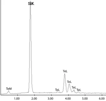
The EDS of the run products on silicon wafers re-vealed only tellurium peaks (Fig. 5). SAED patterns (Fig. 6) obtained from the different product morpholo-gies could all be indexed for the hexagonal structure of tellurium (a⳱ 4.45 Å, c ⳱ 5.92 Å, P312). SAED
pat-terns were taken with the entire tube in the aperture. No multiple diffraction patterns were visible. The tube is most likely a hollow single crystal, although merohedral twinning cannot be excluded. Possible twin operations are a twofold axis parallel to c or a mirror plane parallel
to (110) as known from␣-quartz that has the same space group as tellurium.17,18It is, however, almost impossible to do the necessary dark field imaging to test the presence of twinning because most electrons contributing to the diffraction pattern traverse more than one face of the hexagonal tube. If the hollow crystal would be the result of twinning, they would be diffracted by more than one twin member and possible structure factor differences of equivalent reflections are not usable anymore. The fact that the tubes nucleate on seeds that are not hollow is more in favor of a single crystal than of a twinned crystal. The above twin symmetry operation would be reflected by a stacking fault along the twin boundary. No contrast compatible with such a stacking fault has been observed. The defect concentration, mainly dislocations, is very low. Bright-field images reveal that there are also occa-sional plugs along the tube (Fig. 7). Tellurium micro- and nanotubes remained stable also after storage in air over periods of several months.
The formation of the tubes and rods can best be de-scribed by a nucleation and growth process. Two nuclea-tion events can be distinguished on the silicon substrate. Initially, the evenly distributed hollow seeds (15 seeds/ m2
) form through homogeneous nucleation. Their crys-tallographic orientation seems to be controlled. There is an obvious relationship between the unrelaxed (111) sur-face unit cell of silicon and the basal plane dimensions of the tellurium structure, e.g., 2 asurf
si(111)
⳱ 3 abluk Te
with a mismatch of only 0.9%, leading to preferential nuclea-tion of tellurium with (001) Te parallel to (111) Si (Fig. 8). The growth of the homogeneous nuclei seems to be blocked by the faster growth of nonepitaxial nuclei, which depletes the tellurium concentration close to the substrate. These nuclei are probably tellurium seeds that crystallized already before hitting the substrate. The model proposed for the appearance of well-shaped, hollow, hex-agonal crystals in the wet chemical synthesis route might FIG. 2. Hexagonal tellurium nanotube [detail from Fig. 1 (b)].
FIG. 3. Homogeneously distributed tube-like nuclei on (111) silicon wafer grown in the induction furnace [detail from Fig. 1(b)].
also serve as explanation for the PVD grown tellurium nanocrystals. Preferential attachment of solute atoms at the edges depletes the central portion of the {001} faces. Additional tellurium atoms will continue to attach at these energetically favorable edge sites leading to the observed hollow crystals. In the wet chemical synthesis, hollow crystals were only obtained by keeping the tellu-rium precursor (TeO2) concentration low.
9
This was achieved by adding orthotelluric acid instead of tellurium
dioxide. The slow decomposition kinetics of the acid controlled the oxide concentration and consequently the elemental tellurium concentration. The dilution of the tellurium gas by the argon gas added to the PVD furnace atmosphere might have the same concentration control-ling effect.
The oriented growth of the rods on the aluminum foil, however, seems not to be controlled by crystallography. Similar oriented growth of tubes was observed in the PVD synthesis of carbon nanotubes.19
These tubes were FIG. 4. Tellurium products grown under vacuum (1 × 10⁻⁷mbar) after
25 min of reaction time in the induction furnace: (a) platelets grown on a (111) silicon wafer and (b) nanorods grown on a aluminum foil.
FIG. 5. EDS spectra of a tellurium nanotube.
FIG. 6. Microdiffraction on a tellurium tube deposited on a (111) silicon wafer.
also grown on aluminum substrates, but with additional iron carbide nanocrystals as nucleation seeds. The ori-ented growth was explained by steric hydrance. The only direction of unimpeded growth is perpendicular to the substrate. In the case of tellurium, the rod shape crystal morphology may be explained by the fast growth parallel to the c axis, which is only possible without influence by neighboring crystals for seeds with the c axis perpendicu-lar to the substrate. Reasons for the high density of nu-cleation seeds with the c axis perpendicular to the sub-strate are not clear yet.
B. High vacuum coating system
When PVD was performed in the high vacuum coating system and therefore without the assisting magnetic field used for induction heating, we did not observe the for-mation of tellurium tubes nor rods. This observation is valuable for both type of substrate, for experiments made under vacuum (1.0 × 10⁻⁷
mbar) as well as for experi-ments made after the evacuation of the reaction chamber to 1.0 × 10⁻⁷
mbar and subsequent injection of 1 mbar of Ar and for same reaction times. The products are strictly the same on both substrates. Under vacuum, the products were elemental tellurium platelets, comparable to the ones obtained in the induction furnace under vacuum and on (111) silicon wafer [Fig. 4(a)]. Under 1 mbar Arg,
the products were dendritic tellurium filaments. These results show the importance of the magnetic field as main controlling agent for the growth of tellurium nanotubes.
IV. CONCLUSIONS
Nanostructured tellurium products with different shapes were produced through a simple physical vapor deposition process. By PVD, as described in this paper, the synthesis of tellurium nanotubes is achieved without any template or catalyst. This technique considerably simplifies the subsequent purification process needed with wet chemical synthesis. Moreover, by wet chemical synthesis relative long reaction times are needed.11
The tubular morphology of the run products is depen-dent on the presence of an assisting high frequency mag-netic field and on the atmosphere of the reactor. By con-trolling the reaction time, the aspect ratio of the products can be controlled. PVD-synthesized tellurium crystals exhibit the same rod and tube shaped morphology as observed during wet chemical synthesis. However, PVD allows oriented growth.
Tellurium, selenium and alloys of the two elements are
p-type semiconductors and show piezoelectricity. Their
electric properties have unusual temperature dependen-cies. Selenium has a very high photoconductivity. Tellu-rium and selenium are, moreover, constituents of semi-conductor materials such as CdSe, CdTe, and ZnTe. These interesting electrical properties of tellurium and FIG. 7. Bright-field image of tellurium tubes.
FIG. 8. Unrelaxed (111) silicon surface layer (two atom layer thick) projected along [111]. The silicon atoms describing the indicated hex-agonal array (stippled line) are not at the same level along [111].
tellurium compounds combined with the observed growth morphologies are promising for the fabrication of nanoscale functional devices. The oriented growth of rods, for example, makes tellurium a candidate for elec-tron emitter applications. Emission current measure-ments are currently being undertaken.
ACKNOWLEDGMENTS
We thank Dr. A. Zuettel at the University of Fribourg for useful discussions, C. Neururer at the University of Fribourg for assistance with SEM investigations and technical support, and Dr. M. Dadras at the Service for Microscopy and Nanoscopy at the University of Neuchâ-tel for useful discussions.
REFERENCES
1. S. Iijima: Helical Microtubules of Graphite Carbon Nature 354, 56 (1991).
2. P.J.F. Harris: Carbon Nanotubes and Related Structures, New Materials for the Twenty-first Century (Cambridge University Press, Cambridge, U.K., 1999).
3. P. Gleize, M.C. Schouler, P. Gadelle, and A. Calliet: Growth of tubular BN filaments. J. Mater. Sci. 29, 1575 (1994).
4. N.G. Chopra, H. Luyken, V.H. Crespi, K. Cherrey, A. Zettl, and M.L. Cohen: Synthesis of BN nanotubes. Science 269, 966 (1995).
5. I. Narita and T. Oku: Synthesis of boron nitride nanotubes by using NbB2, YB6and YB6/Ni powders. Diamond Relat. Mater. 12,
1912 (2003).
6. D. Goldberg, A. Rode, Y. Bando, A. Mitome, E. Gamaly, and B. Luther-Davies: Boron nitride nanostructures formed by ultra-high-repetition rate laser ablation. Diamond Relat. Mater. 12, 1226 (2003).
7. R. Tenne, L. Margulis, A. Genut, and G. Hodes: Polyhedral and Cylindrical Structures of WS2. Nature 360, 444 (1992).
8. M. Nath, A. Govindaraj, and C.N.R. Rao: Simple synthesis of MoS2and WS2nanotubes. Adv. Mater. 13, 283 (2001).
9. B. Mayers and Y. Xia: One-Dimensional Nanostructures of Tri-gonal Tellurium with Various Morphologies Can Be Synthesized Using a Solution-Phase Approach. ET J. 12, 1875 (2002). 10. B. Mayers and Y. Xia: Formation of Tellurium Nanotubes
Through Concentration Depletion at the Surfaces of Seeds. Adv. Mater. 14, 279 (2002).
11. G. Wei, Y. Deng, Y-H. Lin, and C-W. Nan: Solvothermal synthe-sis of porous tellurium nanotubes. Chem. Phys. Lett. 372, 590 (2003).
12. X-Y. Liu, M-S. Mo, X-Y. Chen, and Y-T. Qian: A rational redox route for the synthesis of tellurium nanotubes. Inorg. Chem. Comm. (In press).
13. B. Mayers, B. Gates, Y. Yin, and Y. Xia: Large scale Synthesis of Monodisperse Nanorods of Se/Te Alloys Through a Homoge-neous Nucleation and Solution Growth Process. Adv. Mater. 13, 1380 (2001).
14. B. Gates, B. Mayers, Y. Wu, Y. Sun, B. Cattle, P. Yang, and Y. Xia: Synthesis and Characterization of Crystalline Ag2Se
Nanowires through a Template-Engaged Reaction at Room Tem-perature. Adv. Funct. Mater. 12, 679 (2002).
15. Z-Y. Jiang, Z-X. Xie, S-Y. Xie, X-H. Zhang, R-B. Huang, and L-S. Zheng: High purity trigonal selenium nanorods growth via laser ablation under controlled temperature. Chem. Phys. Lett.
368,425 (2002).
16. P. Stadelmann: A Software Package for Electron Diffraction Analysis and HREM Image Simulation in Materials Science Ul-tramicroscopy 21, 131 (1987).
17. A.C. McLaren and P.P. Phakey: Electron microscope study of Brazil twin boundaries in amethyst quartz. Phys. Stat. Sol. 13, 413 (1966).
18. A.C. McLaren and P.P. Phakey: Di.raction contrast from Dau-phine´ twin boundaries in quartz Phys. Stat. Sol. 31, 723 (1969). 19. P. Mauron, C. Emmeneger, and A. Zuettel: Synthesis of oriented
nanotube films by chemical vapor deposition. Carbon 40, 1339 (2002).

![FIG. 2. Hexagonal tellurium nanotube [detail from Fig. 1 (b)].](https://thumb-eu.123doks.com/thumbv2/123doknet/14887095.647441/3.945.492.844.144.412/fig-hexagonal-tellurium-nanotube-detail-from-fig-b.webp)
![FIG. 8. Unrelaxed (111) silicon surface layer (two atom layer thick) projected along [111]](https://thumb-eu.123doks.com/thumbv2/123doknet/14887095.647441/5.945.102.461.133.613/fig-unrelaxed-silicon-surface-layer-layer-thick-projected.webp)
