HAL Id: hal-00610356
https://hal.archives-ouvertes.fr/hal-00610356
Submitted on 25 May 2021
HAL is a multi-disciplinary open access
archive for the deposit and dissemination of
sci-entific research documents, whether they are
pub-lished or not. The documents may come from
teaching and research institutions in France or
L’archive ouverte pluridisciplinaire HAL, est
destinée au dépôt et à la diffusion de documents
scientifiques de niveau recherche, publiés ou non,
émanant des établissements d’enseignement et de
recherche français ou étrangers, des laboratoires
Voltage controlled terahertz transmission through GaN
quantum wells
T. Laurent, R. Sharma, J. Torres, P. Nouvel, S. Blin, L. Varani, Y. Cordier,
M. Chmielowska, Sébastien Chenot, Jp Faurie, et al.
To cite this version:
T. Laurent, R. Sharma, J. Torres, P. Nouvel, S. Blin, et al.. Voltage controlled terahertz transmission
through GaN quantum wells. Applied Physics Letters, American Institute of Physics, 2011, 99 (8),
pp.082101. �10.1063/1.3627183�. �hal-00610356�
arXiv:1105.3131v1 [cond-mat.mes-hall] 16 May 2011
Abstract
We report measurements of radiation transmission in the 0.220–0.325 THz frequency domain through GaN quantum wells grown on sapphire sub-strates at room and low temperatures. A significant enhancement of the transmitted beam intensity with the applied voltage on the devices under test is found. For a deeper understanding of the physical phenomena in-volved, these results are compared with a phenomenological theory of light transmission under electric bias relating the transmission enhancement to changes in the differential mobility of the two-dimensional electron gas.
Voltage controlled terahertz transmission through
GaN quantum wells
T. Laurent, R. Sharma, J. Torres, P. Nouvel, S. Blin, L. Varani, Y. Cordier, M. Chmielowska, S. Chenot, JP Faurie, B. Beaumont, P. Shiktorov, E. Starikov, V. Gruzinskis, V. Korotyevyev, V. Kochelap
February 28, 2018
In the last years, there has been a growing interest in using the terahertz (THz) radiations as a powerful tool to investigate materials/devices/structures in chemistry, biology, physics, medicine and materials science [?]. To develop the electro-optic systems needed by the THz roadmap in the next years [?], it will become mandatory not only to have efficient emitters and detectors available but also solid-state devices able to control and modify THz beam parameters such as intensity, phase, polarization, direction, etc. . . Nowadays GaN quantum wells can be grown with excellent transport properties and a sufficiently high electron-concentration to strongly interact with electromagnetic radiation propagating perpendicularly to the well surface. Since transport properties of the 2D electron gas in the quantum well can be easily controlled by an applied voltage, the possibility to achieve a control of the transmitted radiation is expected.
In this letter we present experimental and theoretical results showing the possibility to control the intensity of THz radiations transmitted through GaN quantum wells by applying low values of dc voltage.
The different layers of the fabricated devices consist of a sapphire substrate, a GaN iron doped template, a GaN 1 µm-thick buffer, a 1 AlN/21 nm-Al0.28Ga0.72N/3 nm-GaN active layer covered with Ti/Al ohmic contacts. The
layers are grown by molecular beam epitaxy and processed as described in [?]. To couple THz waves with the device, we used interdigitated contacts with variable distances between contacts. Here we present results obtained with devices where the distance between contacts are Ls= 19 µm in the short regions
and Ll= 39 µm in the long regions. The width of the device is W = 500 µm.
The experimental set-up uses a commercial electronic source to generate continuous harmonic waves in the 0.220 – 0.325 THz frequency range. The beam is focused in a He-free cryostat by a first spherical mirror. With the simulation of Gaussian beams propagation in this particular frequency domain, we estimated the position of the source needed to obtain the waist in the center of the cryostat where devices are maintained. Further mechanical alignments are performed to optimize the focusing of the beam on the device. The transmitted beam through device is then extracted from the cryostat and focused with the help of a second spherical mirror on a Si-bolometer for measurement. A lock-in amplifier system is used to extract the part of the bolometer signal corresponding
to the transmitted beam. The experimental protocol is the following: first the device is placed into the cryostat at the position defined by the Gaussian beams simulation, and then thermalized. The passive transmission of the bench without an applied dc-bias to the device is thus measured. Then the same transmission spectrum is acquired applying a dc-bias.
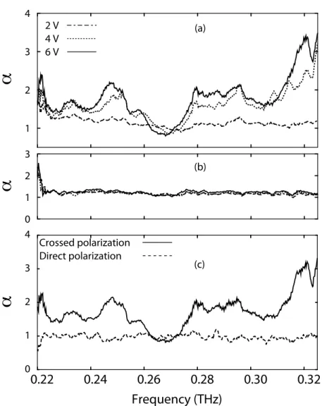
The main results are summarized in Fig. 1, showing the transmission coef-ficient α defined as α(f ) = TB(f )/T0(f ); where f is the frequency, and TB(f )
and T0(f ) are respectively the measured spectra with a bias B and without
bias applied to the device. The applied voltages of investigation vary between 0 and 6 V which correspond to average electric fields in the conduction channel from 0 up to 0.103 and 0.21 kV/cm in the long and short regions of the device respectively. On Fig. 1(a), for measurements performed with the samples main-tained at 77 K, a strong enhancement of the transmitted beam increasing the voltage from 0 to 6 V is found practically in the whole investigated frequency domain. On the opposite, on Fig. 1(b), corresponding to room temperature measurements, no significant dependency with the applied voltage is measured. Moreover, the average value of α at 300 K is near its value at 77 K when 2 V is applied, i.e., when no significant enhancement is measured.
It is noteworthy to emphasize that α depends on the orientation of the sample with respect to the polarization direction of the incident radiation. As shown on Fig. 1(c), if the fingers of the samples are parallel to the polarization direction (i.e. direct polarization), no effect of the bias or temperature (not shown) is found, whereas if the fingers are perpendicular to the polarization direction (i.e. crossed polarization), a maximum effect is found. This situation corresponds to the results presented in Fig. 1(a) and (b).
To interpret on a physical basis the phenomena responsible for the trans-mission enhancement in the sub-THz frequency range we have developed a phenomenological theory of light transmission via device under electrical bias that will be published elsewhere[?]. We modeled its complicated layered struc-ture as a δ-like heavily-doped GaN active layer described by a 2D conductiv-ity σ and a sapphire substrate of thickness h and dielectric constant ǫ. So far as the thicknesses of other undoped layers are much smaller than the sub-THz wavelengths, they can be ignored. We assumed that σ depends on both frequency f and applied voltage U according to the Drude-Lorentz model: σf,U = en
2Dµ
U/(1 − i2πf m∗µU/e), where e is the elementary charge, n
2D
the 2D electron concentration, m∗ the GaN effective mass and µU the
voltage-dependent differential electron mobility. In the framework of this model, ana-lytical expressions for the transmission coefficient α can be obtained following the standard procedure as described in ref. [?]
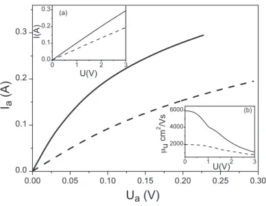
The voltage dependence of µU can be extracted from the electrical
mea-surements of current-voltage characteristics I(U ). From one hand, using the measured I(U ) (see insert (a) of Fig. 2), one can estimate a device global resis-tance R = 15 Ω and R = 9.73 Ω at room and nitrogen temperatures, respec-tively. From the other hand, the active-area resistance Ra can be expressed as
Ra = [1/(en2Dµ0W )][LlLs/(Ll+ Ls)]/N (short and long regions in-parallel),
1 2 3 4 (a) 2 V 4 V 6 V 0 1 2 3
0.22
0.24
0.26
0.28
0.30
0.32
Frequency (THz)
(b)α
α
Crossed polarization Direct polarizationα
0 1 2 3 4 (c)Figure 1: Transmission coefficient as a function of frequency, for a device with Ll = 39 and Ls = 19 µm, for three different biases 2 V, 4 V an 6 V and two
different temperatures: (a) 77 K, and (b) 300 K. (c) Transmission coefficient for two polarizations of the incident beam on the same device at 77 K.
U
a(V)
I
a(A)
U(V) I(A) μu cm 2 /Vs U(V)Figure 2: Current-voltage characteristics related to the active layer of 2D elec-tron gas. Solid and dashed curves correspond to 77 and 300 K, respectively. Insert: (a) Current-voltage characteristics of the whole device and (b) differen-tial mobility as a function of the total applied voltage.
the presence of a 2D electron gas with concentration n2D
≃ 1013 cm−2 and ohmic mobility µ0 ≃ 2000 cm2/(Vs) at room temperature. For liquid nitrogen
temperature we used µ0≃ 6000 cm 2
/Vs according to Ref. [?]. As a consequence, the active-area resistance Raand the contact resistance Rc= R−Raare
respec-tively of 1 and 14 Ω at 300 K and respecrespec-tively of 0.33 and 9.4 Ω at 77 K. The current-voltage characteristics Ia(Ua) of the 2D electron gas shown in Fig. 2
have been extracted using the relations: Ua= U − IRc, Ia = I. At 300 K the
current Iaexhibits only a weak nonlinearity in the whole interval of applied
volt-ages while at 77 K it shows a much more pronounced sub-linear behavior. Such behaviors can be explained by two possibilities: either a pure electron heating or a Joule heating of the whole structure [?]. However, the former possibility should be excluded since it is realized in GaN at fields above few kV/cm [?, ?] while in our case the applied electric fields are of few hundreds of V/cm. A more accurate current-voltage characteristics of the active layer can be obtained tak-ing into account the details of the heat sink and the temperature dependence of the contact resistance. However, at the present stage of investigations, such a task is beyond the scope of our qualitative theory. From the current-voltage characteristics Ia(Ua) we calculated the differential resistance of the active
re-Frequency (THz)
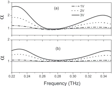
Figure 3: Theoretically calculated transmission coefficient as a function of fre-quency, for U = 1, 2, 3 V at (a) 77 K and (b) 300 K. Calculations are performed assuming a sapphire substrate width h = 350 µm and a dielectric constant ǫ = 12.
gion, then the mobility µU (insert (b) of Fig. 2) and finally the transmission
coefficient α shown in Fig. 3. As seen from Fig. 1 and 3 the theoretical and experimental results are in good agreement. At 300 K both experimental and theoretical α have values in the range 1 − 1.3 in the whole frequency domain and a slight increase with U which is attributed to the weak changes of the differential mobility µU with the applied voltage. At 77 K, µU decreases by a
factor of 6 with increasing bias from 0 to 3 V and therefore, a strong enhance-ment of the transmission is observed. It should be noted that both experienhance-mental and theoretical curves show a frequency window near 0.27 THz where α has a minimum with values around 1 or slightly less then 1. By using the theoretical model, this frequency range is clearly related to radiation interference on the substrate.
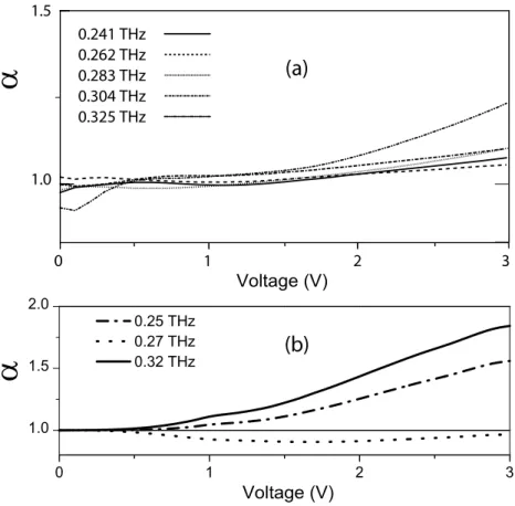
The transmission coefficient as a function of applied voltage exhibits differ-ent behaviors according to the considered frequency as reported in fig. 4. At frequencies outside the interference region the trend of all the curves is to in-crease with applied voltage starting from 1 V. Within the interference region the curves show a slight decrease with the voltage.
In conclusion, an original experimental configuration has allowed measure-ments of the transmitted signal intensity through GaN quantum wells in the 0.220–0.325 THz frequency range. Different effects on the transmission spectra
Figure 4: Experimental (a) and theoretical (b) transmission coefficients as func-tions of applied voltage for three different frequencies f = 0.25, 0.27, 0.32 THz at 77 K.
such as bias conditions and temperature of the device have been investigated and the measured amplification of the transmitted THz radiation has been theo-retically related to a decrease of the differential mobility with the voltage. These results can be considered a promising step toward the development of efficient electro-optic modulators operating in the THz domain.
The French National Research Agency (ANR) is acknowledged for funding this research under contract AITHER no. ANR-07-BLAN-0321. Moreover we acknowledge also the support of TeraLab-Montpellier (GIS CNRS).