The Effect of Atmosphere on Lead Halide
Perovskites
by
Roberto Brenes
B.S. Massachusetts Institute of Technology (2017)
Submitted to the Department of Electrical Engineering and Computer
Science
in partial fulfillment of the requirements for the degree of
Master of Engineering in Electrical Engineering and Computer Science
at the
MASSACHUSETTS INSTITUTE OF TECHNOLOGY
February 2019
c
○ Massachusetts Institute of Technology 2019. All rights reserved.
Author . . . .
Department of Electrical Engineering and Computer Science
January 29, 2019
Certified by . . . .
Vladimir Bulović
Professor of Electrical Engineering and Computer Science
Thesis Supervisor
Accepted by . . . .
Katrina LaCurts
Chair, Master of Engineering Thesis Committee
The Effect of Atmosphere on Lead Halide Perovskites
by
Roberto Brenes
Submitted to the Department of Electrical Engineering and Computer Science on January 29, 2019, in partial fulfillment of the
requirements for the degree of
Master of Engineering in Electrical Engineering and Computer Science
Abstract
Metal halide perovskites are exciting materials for low-cost optoelectronic devices such as solar cells and LEDs. At present, perovskite materials still suffer from sub-stantial non-radiative decay, particularly under solar illumination conditions, and are therefore yet to reach their full potential. In this thesis, we demonstrate the use of light and atmospheric treatments on polycrystalline perovskite films, resulting in minimal non-radiative losses and properties approaching those of perovskite single crystals and even the best crystalline semiconductors reported to date. We show that by combining light and atmospheric treatments, we can increase the internal lu-minescence quantum efficiencies of polycrystalline perovskite films from 1% to 89%, with carrier lifetimes of 32 𝜇s and diffusion lengths of 77 𝜇m, comparable with per-ovskite single crystals. Remarkably, the surface recombination velocity of holes in the treated films is 0.4 cm/s, approaching the values for passivated crystalline sili-con, which has the lowest values for any semiconductor to date. The enhancements translate to solar cell power-conversion efficiencies of 19.2%, with a near-instant rise to stabilized power output, consistent with suppression of ion migration. Also, we use in-situ microphotoluminescence measurements to elucidate the impact of light-soaking individual methylammonium lead iodide grains while immersing them with different atmospheric environments. We show that emission from each grain depends sensitively on both the environment and the nature of the specific grain, i.e., whether it shows good (bright grain) or poor (dark grain) luminescence properties. We find that the dark grains show substantial rises in emission, while bright grain emission is steady when illuminated in the presence of oxygen and/or water molecules. We find that oxygen molecules bind particularly strongly to surface iodide vacancies which, in the presence of photoexcited electrons, lead to efficient passivation of the carrier trap states that arise from these vacancies. This thesis reveals a unique insight into the nature of nonradiative decay and the impact of atmospheric passivation on the macro- and micro-scale properties of perovskite films.
Thesis Supervisor: Vladimir Bulović
Acknowledgments
I want to thank, first and foremost, my parents Fernando and Adelita for all their support throughout my life. Without their love, education and guidance I would not be anywhere close to where I am now. It also would not have been possible without the unconditional love from my siblings, Eduardo, Nano and Carolina who are an integral part of my life. Bhalu, my dog, should also get a mention for making our home even happier than what it already was.
Tuto, Dan, Thomas and all my other friends, thank you for being an invaluable part of my life and for all the support throughout this whole process.
I would also like to thank my advisors, Vladimir Bulović and Samuel Stranks for their guidance throughout undergraduate and graduate life. Their drive and support has been second to none in pushing me to be better scientist.
This work was completed with the help of all my past and present coworkers in ONELab, whom I would like to acknowledge for the valuable discussions, advice and all the enjoyable moments we have spent together. Maddie, Dane, Panda, Melissa, Michel, Joel, Max, Rich, Mayuran, Farnaz, Mengfei, Ella, Ryan, Tom, Anna, Annie, Melany, Melody and all the others, I want to thank you for being an important part of my academic life.
Finally, I would like to acknowledge all of those outside of MIT who have con-tributed to these projects and made this thesis possible: Sandeep Pathak, Eline Hutter, Saiful Islam, Nakita Noel, Christopher Eames, Dengyang Guo, Henry Snaith, Tom Savenije and Sir Richard Friend.
Contents
1 Introduction 29
1.1 Confocal Microscopy . . . 30
1.2 Time-correlated single photon counting . . . 34
1.3 Thesis Outline . . . 36
2 Metal Halide Perovskite Polycrystalline Films Exhibiting Properties of Single Crystals 37 2.1 Introduction . . . 37
2.2 Results . . . 38
2.2.1 Macro- and Micro-photoluminescence Enchancements . . . 38
2.2.2 Enhancements in Film Photoconductance and Diffusion Length 41 2.2.3 Enhancements in Solar Cell Device Performance . . . 45
2.2.4 Mechanism of Photobrightening . . . 47 2.3 Discussion . . . 48 2.4 Experimental Procedures . . . 50 2.4.1 Sample Preparation . . . 50 2.4.2 Macro-photoluminescence Measurements . . . 51 2.4.3 Micro(Confocal)-photoluminescence Measurements . . . 52
2.4.4 Time-Resolved Microwave Conductivity Measurements . . . . 52
2.4.5 Device Fabrication and Characterization . . . 53 3 The Impact of Atmosphere on the Local Luminescence Properties
3.1 Introduction . . . 57
3.2 Results . . . 60
3.2.1 Local Grain Luminescence Under N2 . . . 60
3.2.2 Local Grain Luminescence Under O2 . . . 61
3.2.3 Local Grain Luminescence After Humidity Exposure . . . 63
3.2.4 Density Functional Theory Calculations . . . 65
3.3 Discussion . . . 68
3.4 Experimental Section . . . 70
3.4.1 Photoluminescence Measurements . . . 70
3.4.2 Ab-initio Calculations . . . 71
4 Conclusion 73 A Supplementary Information to Chapter 2 75 A.1 Kinetic Model . . . 75
A.2 Importance of combination of light, oxygen and humidity . . . 82
A.3 Sensitivity of reported values . . . 100
A.4 Extracting relative fractions of 𝑘𝑅 and 𝑘𝑛 . . . 102
A.5 Surface recombination velocity . . . 103
A.6 Ab-initio calculations . . . 103
A.7 Surface characterization . . . 104
A.8 Device external quantum efficiency (EQE) measurements . . . 105
List of Figures
1-1 Standard confocal microscope setup as depicted by Semwogerere et al.[71]. . . 31
1-2 Left: Airy Disc intensity distribution. Right: Intensity distribution 𝑝𝑐𝑜𝑛𝑓 for a typical confocal setup. Plots from Robert H. Webb[88]. . . 33
1-3 a) Scheme for measuring photon arrival times. b) Histogram built from the photon arrival times [86]. . . 35
1-4 Typical TCSPC setup as detailed by Michael Wahl. An ND filter is used to reduce the intensity of the laser and a cutoff filter (normally a dichroic filter) to remove any scattered light from the laser and only collect the wavelengths of interest [86]. . . 35
2-1 Macro- and Micro-photoluminescence Enhancements of Thin Films un-der Solar Illumination Conditions (a–c) Internal PLQE 𝜂 measure-ments over time under illumination with a CW 532-nm laser at an excitation intensity equivalent to 2 sun (150 mW/cm2) in dry N2 (a),
dry air (b), and humid air (c). Inset: Time-resolved PL decays of the films after the stated treatment with pulsed excitation at 405 nm (exci-tation density of 5.4 × 1015cm−3). (d–h) In situ confocal PL maps with 405-nm excitation measured in (d) dry air, (e) humidified air, (g) after light soaking for 10 min under excitation with a 532-nm laser equiva-lent to 10 sun under humid air, (g) after returning to dry air, and (h) measured the next day with storage in dry air. Insets to (d) and (g): emission stability of the films in dry air before and after the treatment, respectively, with excitation at 532-nm at intensity equivalent to 10 sun. 40
2-2 Enhancements in Film Photoconductance Determined from Time-Resolved Microwave Conductivity Measurements (a) Photoconductance mea-surements for a MAPbI3 film after storage in dry air and after being
subjected to light soaking for 30 min in humid air (40% humidity) under a constant photon flux similar to solar conditions. The TRMC trace taken after storing the same sample in a nitrogen glove box for a week after the treatment is also shown. The TRMC decays were recorded by photo-exciting the samples in dry N2 with pulsed
illumi-nation at 500 nm and an excitation density of 5×1014cm−3. (b) TRMC decays (normalized to absorbed flux) of the treated samples with the initial charge excitation density as indicated. (c) Dashed lines are fits to the data using the trap model summarized in (c), where 𝐺𝑐 is the
generation rate and 𝑘𝑇 and 𝑘𝐷 are the trapping and trap
recombina-tion rates, respectively. (d) Diffusion lengths of the electrons and holes before and after the treatments. . . 42
2-3 Enhancements in Solar Cell Device Performances (a) Light and dark J-V curves of champion devices for the devices containing untreated (stored in dry air) and treated (light soaked in humid air) films mea-sured under AM1.5 100 mW/cm2 simulated sunlight. (b) Stabilized
power output of the devices presented in (a) measured by holding the devices at their maximum power point (as determined from J-V curves) for 50 s. . . 46
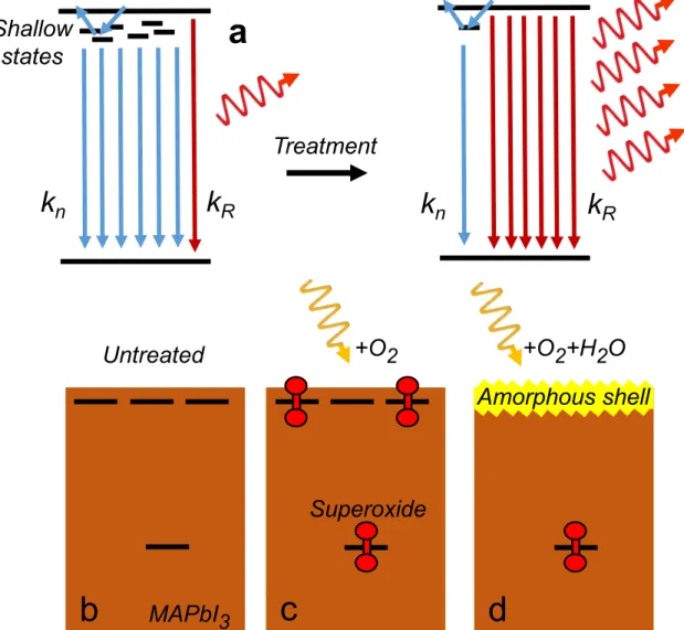
2-4 Mechanism of Photobrightening (a) Schematic showing non-radiative recombination (𝑘𝑛) dominating owing to shallow surface states, which
are removed in the treatment to lead to radiative-dominant (𝑘𝑅)
recom-bination. (b–d) Untreated MAPbI3 films (b) containing non-radiative
trap states that are passivated by exposure of MAPbI3 to (c) light and
oxygen and (d) light, oxygen, and water. . . 49
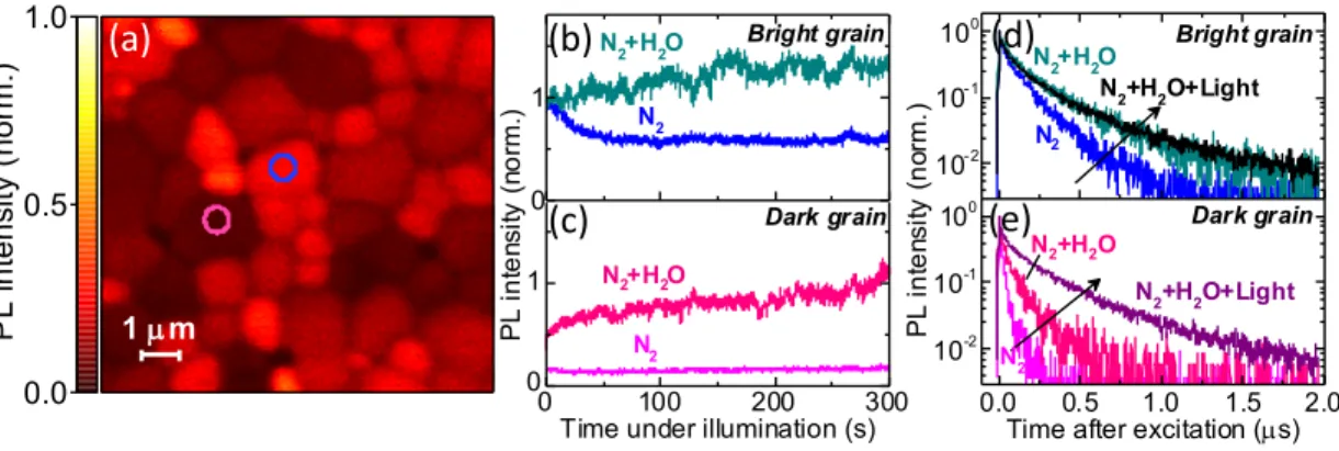
3-1 Microscale photoluminescence properties in dry and humid nitrogen. (a) Confocal PL map of a MAPbI3 perovskite film in dry nitrogen
nor-malised to the maximum intensity. (b, c) Monitoring the PL intensity (emission count rate) over time under illumination from (b) a bright grain (blue circle in a) and (c) a dark grain (pink circle in a) under dry nitrogen and under humidified ( 45% relative humidity) nitrogen. The PL intensity for each trace over time is given relative to the starting value for the bright grain in nitrogen, which is normalised to 1. (d, e) PL decays from the same (d) bright and (e) dark grains under dry nitrogen, and before and after light soaking in humidified nitrogen. Samples were photoexcited with a 405 nm laser with a repetition rate of 0.5 MHz and a fluence of ∼ 1 𝜇J/cm2/pulse (∼500 mW/cm2), and this same laser was used for local light-soaking (total photon dose of ∼150 J/cm2). . . . 61
3-2 Microscale photoluminescence properties in dry and humid air. (a) Confocal PL map of a MAPbI3 perovskite film in dry air normalised to
the maximum intensity. (b, c) Monitoring the emission (PL count rate) over time under illumination from (b) a bright grain (blue circle in a) and (c) dark grain (pink circle in a) under dry air and under humidified ( 45% relative humidity) air. The PL intensity for each trace over time is given relative to the starting value for the bright grain in air, which is normalised to 1. (d, e) PL decays from the same (d) bright and (e) dark grains under dry air before and after the light-soaking. (f, g) PL decays from the same (f) bright and (g) dark grains under dry air, humidified air, and after the light-soaking in humidified air. Samples were photoexcited with a 405 nm laser with a repetition rate of 0.5 MHz and a fluence of ∼1 𝜇J/ cm2/pulse (∼500 mW/cm2), and this same laser was used for local light-soaking (total photon dose of ∼150 J/cm2). . . 62
3-3 Local grain emission stability after humidity exposure. (a) Confocal PL map of a MAPbI3 perovskite film in dry air following exposure to
humid air for 60 minutes, normalised to the same intensity value as Fig. 3-2A to allow direct comparison. (b) Monitoring the emission intensity (count rate) from various bright and dark grains denoted in (a) over time under illumination, normalised to the intensity of the same grain as in Fig. 3-2b. Inset: emission from the same grains under continuous illumination before the exposure to humidity. (c) Confocal PL map of a MAPbI3 perovskite film in dry nitrogen following exposure to humid
nitrogen for 60 minutes, normalised to the same intensity value as Fig. 3-1a. (d) Monitoring the emission intensity (count rate) from various bright and dark grains denoted in (c) over time under illumination, normalised to the intensity of the same grain as in Fig. 3-1b. Samples were photoexcited with a 405 nm laser with a repetition rate of 0.5 MHz and a fluence of ∼1 𝜇J/cm2/pulse (∼500 mW/cm2), and this same laser was used for local lightsoaking (total photon dose of ∼150 J/cm2). . . 64
3-4 Surface atomic and electronic structures. Schematic of the local atomic-scale configurations of the surface termination layer (top row) and cal-culated band structures (bottom row) for the (110) surface of MAPbI3.
(a) Pristine uncharged surface, (b) negatively-charged iodine vacancy into which the following molecules are adsorbed; (c) N2, (d) H2O and
(e) O2. Key: purple - iodine, grey - lead, blue - nitrogen, red - oxygen,
white - hydrogen. We note that our calculations explicitly included excess electrons; hence the Fermi level (red line) is above any trap states because those states are filled. See Figures B-6 to B-9 for other configurations. . . 68
A-1 Schematic of the recombination and generation pathways in the kinetic model (a) with photon recycling and (b) when excluding the effects of photon recycling. 𝐺𝑐is the generation rate, 𝑘𝑅is the radiative
bimolec-ular rate, 𝑘𝑛 is the non-radiative bimolecular rate, 𝑘𝑇 is the trapping
rate, 𝑘𝐷 is the trap depopulation rate, 𝑁𝑡 is the deep trap density, 𝑝0
is the background hole density [39], 𝜂𝑒𝑠𝑐 is the escape probability of
photons [68]. . . 76 A-2 (a-d) External PLQE 𝜂𝑚𝑒𝑎𝑠 measurements over time under
illumina-tion with a 532-nm laser at an excitaillumina-tion intensity equivalent to ∼2 sun (∼150 mW/cm2) in (a) dry nitrogen, (b) dry compressed air, (c)
humidified compressed air, and (d) after returning to dry compressed air. (e-h) show the same plots but after converting the external values to internal PLQE 𝜂. . . 77 A-3 Time-resolved PL decays of the (a) untreated (dry N2) and (b) treated
(humid air + light, where light is equivalent to 1 sun illumination intensities) samples. Samples were excited with a 405-nm pulsed laser with the stated excitation densities (realized through use of optical filters) and a repetition rate of 20 kHz. . . 78 A-4 In-situ confocal PL maps measured in (a) dry N2, and (b) after light
soaking for 10 minutes under excitation with a 532-nm laser equivalent to ∼10 sun under dry N2. (c-d) Show the same measurements under
dry air. PL maps were collected by photo-exciting with a 405-nm laser with a repetition rate of 0.5 MHz and a fluence of ∼1 𝜇J/cm2/pulse. 79 A-5 (a) Emission of the films in Figure A-4a and c in dry air and dry
nitro-gen during the light-soaking with excitation at 532-nm and intensity equivalent to ∼10 sun. (b, c) Histograms showing the distribution of average lifetimes corresponding to the respective maps in Figure A-4. (d, e) Histograms showing the distribution of emission intensities corresponding to the respective maps in Figure A-4. . . 80
A-6 (a) Emission of the films in Fig. 2-1d-h during the light-soaking with excitation at 532-nm and intensity equivalent to ∼10 sun under the stated atmospheric conditions. (b) The PL decays summed across the map before the treatment (cf. Fig. 2-1d) and after the treatment with light, air and humidity (cf. Fig. 2-1g). The corresponding distributions of the average lifetime and intensity are shown in (c) and (d), respectively. 81
A-7 PL stability immediately after the treatment (red) and after 3 weeks of storage in a nitrogen-filled glove box for a (a) bare film and (b) film coated with a spin-coated layer of PMMA. . . 82
A-8 In-situ confocal PL maps measured in (a) dry air, (b) humidified air, (c) after returning to dry air (i.e. without any light soaking). PL maps were collected by photo-exciting with a 405-nm laser with a repetition rate of 0.5 MHz and a fluence of ∼1 𝜇J/cm2/pulse. (d) Histograms of the intensity distribution of each map. These distributions should be compared to those in Figure A-6, where illumination under humidity leads to substantial increases in the intensity. . . 83
A-9 External PLQE 𝜂𝑚𝑒𝑎𝑠measurements over time under illumination with
a 532-nm laser at an excitation intensity equivalent to ∼2 sun (∼150 mW/cm2) in nitrogen (black) and compressed air (red) under (a) dry
conditions, (b) humid conditions, and (c) after returning to dry condi-tions. The effects are far better retained for the sample light-soaked in air and humidity. . . 84
A-10 PL measurements over time under illumination with a 532-nm laser at an excitation intensity equivalent to ∼2 sun (∼150 mW/cm2) in
A-11 (a) Photoconductance measurements for a MAPbI3 film after storage
in dry nitrogen and then after being subjected to light-soaking for 30 minutes in dry nitrogen under a white light LED source generating a similar photon flux to AM1.5 sunlight. The TRMC decays were taken by photo-exciting the samples in dry N2 with pulsed
illumina-tion at 500 nm and an excitaillumina-tion density of 4.75 × 1014cm−3. The
inset shows the half lifetimes of the corresponding decays at different excitation densities (other decays not shown here). The other pan-els show similar measurements but under the stated atmosphere and conditions, i.e. (b) humid nitrogen (40% relative humidity) (excita-tion density of 4.93 × 1014cm−3), (c) dry air (excitation density of 3.87 × 1014cm−3) and (d) humid air (40% relative humidity)
(excita-tion density of 5.07 × 1014cm−3). Panels b and d also show the decays taken after storing the same sample in a nitrogen-filled glove box for various times after treatment. . . 86
A-12 Excitation-dependent TRMC decays of the (a) untreated samples and (b) samples 1 week after treatment (with storage in a nitrogen-glove box in between), with the initial charge excitation density (pulsed il-lumination at 500 nm) as shown in the legends. Dashed lines are fits to the data using the trap model described in Chapter 2. The corre-sponding data for the freshly-treated sample are shown in Figure 2-2b 87
A-13 The effective TRMC decay curves for each stated treatment for elec-trons (dashed lines) and holes (solid lines) decoupled using the rate equations in the trapping model incorporating electron traps 𝑁𝑡 [7]
(Scheme A-1) when including photon recycling (𝑘𝑒𝑓 𝑓2 = 𝜂𝑒𝑠𝑐𝑘𝑅+ 𝑘𝑛)
(a-c) and when subtracting off the effects of photon recycling (𝑘𝑖𝑛𝑡 2 =
A-14 Half lifetime of the electron and holes extracted from the decays in Figure A-13a-c with photon recycling (a) and Figure A-13d-f without photon recycling (b). We use these lifetimes to calculate the resulting diffusion length of each carrier using 𝐿𝐷 =√︀𝑘𝐵𝑇 𝜇𝜏1/2/𝑒, where 𝑘𝐵 is
the Boltzmann constant, 𝑇 the temperature, 𝑒 the electron charge and 𝜇 the mobility extracted from the photo-conductance measurements. The diffusion lengths are shown with (c) and without photon recycling (d). The diffusion lengths in the former case are interpreted as the cu-mulative diffusion length of a charge carrier including photon recycling events (but not including distance travelled by photons until reabsorp-tion), while the latter is interpreted as the diffusion length of a charge carrier from initial excitation to first recombination event. . . 89
A-15 (a) Light and dark J-V curves of champion devices for the devices containing acetonitrile-based films stored in dry air, humid air (45% relative humidity), and light-soaked under dry air and humid air for 20 minutes with a white light LED array with an intensity similar to simulated sunlight. Device measurements were taken under AM1.5 100mW/cm2 simulated sunlight and the presented scans were measured
scanning from 1.4 V to 0 V (open-circuit to short-circuit, OC-SC). The comparison of the curves scanning from OC-SC and then from SC-OC are presented in (b), showing that there is some hysteresis in the devices under these scan conditions but this effect is reduced for the treated sample. . . 90
A-16 (a-d) Device performance statistics for devices containing acetonitrile-based films stored in dry air in the dark (DAD), light-soaked in dry air (DAL), stored in humid air (45% relative humidity) in the dark (HAD) and light-soaked under humid air (45% relative humidity) (HAL). The light-soaking treatments were performed in the stated conditions by illuminating with a white-light LED array with an intensity similar to simulated sunlight for 20 minutes. Device measurements were taken under AM1.5 100mW/cm2 simulated sunlight. . . . 91
A-17 Stabilized maximum power output for devices containing acetonitrile-based films stored in (a) dry air in the dark (DAD), (b) light-soaked in dry air (DAL), (c) stored in humid air (45% relative humidity) in the dark (HAD) and (d) light-soaked under humid air (45% relative humidity). The light soaking treatments were performed in the stated conditions by illuminating the half-constructed devices with a white light LED array with an intensity similar to simulated sunlight for 20 minutes. The measurements were taken by holding at the maximum power point voltage and measuring current under AM1.5 100mW/cm2 simulated sunlight. . . 92
A-18 (a) Light and dark J-V curves of champion devices for the devices con-taining acetonitrile-based films stored in dry air in the dark (DAD) and light-soaked in humid air (45% relative humidity) for 20 minutes with a white light LED array with an intensity similar to simulated sunlight (HAL). The measurements were taken fresh after the treatments and then after storage in a nitrogen-filled glove box for 3 weeks and 8 weeks. Device measurements were taken under AM1.5 100mW/cm2 simulated
sunlight. (b) External quantum efficiency (EQE) measurements on the devices stored for 8 weeks showing the integrated currents match those obtained from the current-voltage curves. . . 93
A-19 Light and dark J-V curves of champion devices for the devices con-taining acetate/HPA-based films stored in dry nitrogen (DND), dry air (DAD), humid air (45% relative humidity, HAD), and light-soaked under dry nitrogen (DNL), dry air (DAL) and humid air (HAL) for 20 minutes with a white light LED array with an intensity similar to simulated sunlight. Device measurements were taken under AM1.5 100mW/cm2 simulated sunlight. . . 94
A-20 L(a-d) Device performance statistics for devices containing acetate-based films stored in dry nitrogen in the dark (N2D), light-soaked in dry nitrogen (N2L), dry air in the dark (DAD), light-soaked in dry air (DAL), stored in humid air (45% relative humidity) in the dark (HAD) and light-soaked under humid air (45% relative humidity) (HAL). The light soaking treatments were performed in the stated conditions by illuminating with a white light LED array with an intensity similar to simulated sunlight for 20 minutes. Device measurements were taken under AM1.5 100mW/cm2 simulated sunlight. . . 95
A-21 Stabilized maximum power output for devices containing acetate/HPA-based films stored in (a) dry nitrogen in the dark (DND), (b) light-soaked in dry nitrogen (DNL), (c) dry air in the dark (DAD), (d) light-soaked in dry air (DAL), (e) stored in humid air (45% relative humidity) in the dark (HAD) and (f) light-soaked under humid air (45% relative humidity). The light soaking treatments were performed in the stated conditions by illuminating the half-constructed devices with a white light LED array with an intensity similar to simulated sunlight for 20 minutes. These measurements were taken by holding the full devices at the maximum power point voltage and measuring current under AM1.5 100mW/cm2 simulated sunlight. . . 96
A-22 Electronic structure of MAPbI3 (001) surface calculated by density
functional theory. (a) band structure and D.O.S. for (001) surface containing an iodine vacancy occupied by a photogenerated electron showing shallow trap states below the conduction band. (b) band structure and D.O.S. for (001) surface containing an iodine vacancy occupied by a photogenerated electron into which an O2 molecule is
chemisorbed and reduced to form a superoxide species O−2. The sub gap shallow trap states indicated in (a) are now significantly reduced in density. . . 97
A-23 (a) PL measurements over time under illumination with a 532-nm laser at an excitation intensity equivalent to ∼2 sun (∼150 mW/cm2) in dry air (blue) and humidified air (red). (b) X-Ray Photoemission Spec-troscopy (XPS) measurements of the (b) I3d, (b) O1s, (d) N1s, (e) C1s, (f) Pb4f signatures in the regions of the sample light-soaked (light) and regions of the same films without light-soaking (dark). The atomic percent of oxygen species is labelled for each treatment. We find an increase in the O content after light-soaking in dry air, a substantial further increase in O when bringing into humid air, and a further in-crease again after light-soaking in humid air for 1000 seconds. We note that these O1s peaks are broad and likely consist of a range of species including, among others, superoxides and hydroxides. We do not ob-serve dramatic changes in the other species, nor in the peak positions of each species. . . 98
A-24 Atomic force microscopy (AFM) images of the films for (a) a film stored in dry air without any light and (b) a region illuminated in humid air for 10 minutes with a 532-nm laser at an excitation intensity equivalent to ∼2 sun (∼150 mW/cm2). The root-mean-square (RMS) variations
of the surface over larger scan areas excluding pin-holes is 40.2 ± 4.0 nm (dry air) and 44.5 ± 4.5 nm (humid air + light). This represents a negligible change in roughness though potentially a very slight textur-ing after exposure to humidity and light. We note that this increase could not explain the increased external PLQE measurements we observe. 99
A-25 (a) PL measurements over time under illumination with a 532-nm laser at an excitation intensity equivalent to ∼2 sun (∼150 mW/cm2) in dry
air. (b-c) In-plane grazing incidence X-Ray Diffraction (IP-GIXD) for the (b) light-soaked region of a and (c) another region of the same sam-ple without light-soaking (dark). (d-f) The same series but with humid air conditions. We do not find any significant changes after treatment in atmosphere or light for the short soaking periods in which we see the PL enhancements, suggesting we are not substantially perturbing the surface crystallinity or creating crystalline surface material. Sig-nificantly, no PbI2 is detected (expected ∼ 12.5∘). . . 100
B-1 PL decays from the same bright and dark grains shown in Figure 3-1a, before and after light soaking in dry nitrogen. Samples were photoex-cited with a 405 nm laser with a repetition rate of 0.5 MHz and a fluence of ∼1 𝜇J/cm2/pulse (∼500 mW/cm2), and this same laser was
B-2 Compressed air storage over time in the dark. Confocal PL map of MAPbI3 films prepared in a nitrogen glove box and maps acquired
(a) in dry nitrogen, and in dry air after (b) 1 hour, (c) 24 hours and (d) 48 hours in dry compressed air. (e) A film stored for 48 hours in dry air but then measured in dry nitrogen after 1 hour storage in dry nitrogen, suggesting the oxygen pre-soaking (loading) effects can be removed. The map intensities are given relative to the maximum value in (a), which is normalised to 1. Samples were photoexcited with a 405 nm laser with a repetition rate of 0.5 MHz and a fluence of ∼1 𝜇J/cm2/pulse (∼500 mW/cm2). (f) Total summed intensity of each
map relative to the summed intensity of (a), which is normalised to 1. The blue symbol corresponds to the map in (e). . . 109
B-3 PL from a MAPbI3 film measured in-vacuo (pressure < 10−4 mbar)
under continuous illumination with a 532-nm laser with excitation den-sity similar to solar illumination conditions (∼2 sun, 150 mW/cm2). . 110
B-4 (a) Confocal PL map of a MAPbI3 perovskite film in dry air
nor-malised to the maximum intensity. (b) Monitoring the emission inten-sity (count rate) from various bright and dark grains denoted in (a) over time under illumination in dry air. The PL intensity for each trace over time is given relative to the starting value for the highest initial intensity (blue grain), which is normalised to 1. These correspond to the same grains as shown in Figure 3-3a and b but before the expo-sure to humidity (cf. Figure 3-2). Samples were photoexcited with a 405 nm laser with a repetition rate of 0.5 MHz and a fluence of ∼1 𝜇J/cm2/pulse (∼500 mW/cm2), and this same laser was used for local
B-5 (a) Confocal PL map of a MAPbI3 perovskite film in dry air
nor-malised to the maximum intensity. (b) Monitoring the emission in-tensity (count rate) from the same grain while light-soaking in dry air (cyan), humid air (blue) and after returning the sample to dry air (purple). This grain is unstable while light-soaking in humid air but retains its emission stability after returning to dry air. The emission intensities were normalised to the same initial value as the dry air mea-surement in Fig. 3-3c. Samples were photoexcited with a 405 nm laser with a repetition rate of 0.5 MHz and a fluence of ∼1 𝜇J/cm2/pulse (∼500 mW/cm2), and this same laser was used for local light-soaking
(total photon dose of ∼150 J/cm2). . . 114
B-6 Electronic structures and density of states (DOS) for the (110) sur-face of MAPbI3 in the absence of any molecules. Columns 1, 2 and 3
correspond to the vacancies being negatively, neutral, and positively charged, respectively. (a)-(c) (row 1) corresponds to surface sites above Pb2+ on the PbI2-terminated surface and (d)-(f) (row 2) in an iodine
vacancy on defect-rich PbI2 surface terminations. In the band
struc-tures the Fermi level is indicated by a red line. . . 115
B-7 Electronic structures and density of states (DOS) for the (110) surface of MAPbI3 with adsorption of N2. Columns 1, 2 and 3 correspond
to the vacancies being negatively, neutral, and positively charged, re-spectively. (a)-(c) (row 1) corresponds to surface sites above Pb2+ on the PbI2-terminated surface and (d)-(f) (row 2) in an iodine vacancy
on defect-rich PbI2 surface terminations. In the band structures the
B-8 Electronic structures and density of states (DOS) for the (110) surface of MAPbI3 with adsorption of H2O. Columns 1, 2 and 3 correspond
to the vacancies being negatively, neutral, and positively charged, re-spectively. (a)-(c) (row 1) corresponds to surface sites above Pb2+ on the PbI2-terminated surface and (d)-(f) (row 2) in an iodine vacancy
on defect-rich PbI2 surface terminations. In the band structures the
Fermi level is indicated by a red line. . . 116 B-9 Electronic structures and density of states (DOS) for the (110) surface
of MAPbI3 with adsorption of O2. Columns 1, 2 and 3 correspond
to the vacancies being negatively, neutral, and positively charged, re-spectively. (a)-(c) (row 1) corresponds to surface sites above Pb2+ on the PbI2-terminated surface and (d)-(f) (row 2) in an iodine vacancy
on defect-rich PbI2 surface terminations. In the band structures the
Fermi level is indicated by a red line. . . 117 B-10 (001) Surface atomic and electronic structures. Local atomic
configura-tion in surface terminaconfigura-tion layer (top row) and band structure (bottom row) for the (001) surface of MAPbI3 (cf. Figure 3-4 for (110) results).
(a) Pristine uncharged surface, (b) negatively-charged iodine vacancy into which the following molecules are adsorbed; (c) N2, (d) H2O and
(e) O2. Key: purple - iodine, grey - lead, blue - nitrogen, red - oxygen,
white - hydrogen. In the band structures the Fermi level is indicated by a red line. . . 117 B-11 Electronic structures and density of states (DOS) for the (001)
sur-face of MAPbI3 in the absence of any molecules. Columns 1, 2 and 3
correspond to the vacancies being negatively, neutral, and positively charged, respectively. (a)-(c) (row 1) corresponds to surface sites above Pb2+ on the PbI2-terminated surface and (d)-(f) (row 2) in an iodine
vacancy on defect-rich PbI2 surface terminations. In the band
B-12 Electronic structures and density of states (DOS) for the (001) surface of MAPbI3 with adsorption of N2. Columns 1, 2 and 3 correspond
to the vacancies being negatively, neutral, and positively charged, re-spectively. (a)-(c) (row 1) corresponds to surface sites above Pb2+ on the PbI2-terminated surface and (d)-(f) (row 2) in an iodine vacancy
on defect-rich PbI2 surface terminations. In the band structures the
Fermi level is indicated by a red line. . . 119 B-13 Electronic structures and density of states (DOS) for the (001) surface
of MAPbI3 with adsorption of H2O. Columns 1, 2 and 3 correspond
to the vacancies being negatively, neutral, and positively charged, re-spectively. (a)-(c) (row 1) corresponds to surface sites above Pb2+ on the PbI2-terminated surface and (d)-(f) (row 2) in an iodine vacancy
on defect-rich PbI2 surface terminations. In the band structures the
Fermi level is indicated by a red line. . . 120 B-14 Electronic structures and density of states (DOS) for the (001) surface
of MAPbI3 with adsorption of O2. Columns 1, 2 and 3 correspond
to the vacancies being negatively, neutral, and positively charged, re-spectively. (a)-(c) (row 1) corresponds to surface sites above Pb2+ on the PbI2-terminated surface and (d)-(f) (row 2) in an iodine vacancy
on defect-rich PbI2 surface terminations. In the band structures the
Fermi level is indicated by a red line. . . 121 B-15 Effect of vacancy charge state on photobrightening. Effect of iodine
vacancy charge state on the photobrightening effect in an oxygen at-mosphere on the (001) surface. All three types of surface vacancy (a-c) possess trap states. The photobrightening effect increases in the order: (d) positively charged, (e) neutral and (f) negatively charged (where we judge the effect by the final DOS near the Fermi level). In dark conditions all three charge states are possible but the intrinsic vacancy concentration will be much lower due to photo-induced iodine vacancy creation in the illuminated case. . . 122
List of Tables
2.1 Summary of Parameters from TRMC Measurements and Fits for Thin Films of MAPbI3 Untreated and Treated . . . 43
3.1 Adsorption energies of N2, H2O, and O2molecules onto iodine vacancies
on a PbI2-terminated (110) surface of MAPbI3, with the vacancy in
three possible charge states due to photoexcitation. See Table B.1 for adsorption energies for binding to Pb2+ on the PbI2-terminated surface
and Table B.2 for the (001) configuration . . . 67 A.1 Relevant parameters extracted from the fits to the data with the kinetic
model for the untreated (Figure A-12a) and treated (Fig. 2-2b) films, and 1 week after treatment (Figure A-12b). . . 101 B.1 Adsorption energies of N2, H2O, and O2 molecules on the (110)
sur-face of MAPbI3 in three possible charge states due to photoexcitation.
Favourable surface sites are on the Pb2+ on the PbI2-terminated
sur-face and in an iodine vacancy on defect-rich PbI2 surface terminations. 111
B.2 Adsorption energies of N2, H2O, and O2 molecules on the (001)
sur-face of MAPbI3 in three possible charge states due to photoexcitation.
Favourable surface sites are on the Pb2+ on the PbI2-terminated
Chapter 1
Introduction
The human’s population demand for energy has increased almost two-fold in the past 30 years [12] and shows no sign of slowing down. At the same time, climate change, largely due to human CO2 emissions from fuel sources has threatened the way of
life for future generations [50]. In order to meet the energy demand and mitigate climate change, renewable energy sources must become predominant in the future. Photovoltaic devices represent one of the key renewable energy sources since the sun is the largest source of energy available to humans. The International Energy agency estimates that the total global energy consumption by 2035 will be approximately 20 TW, which could be easily satisfied if we harnessed even a fraction of the 89,000 TW of power from the Sun incident on Earth [41].
Crystalline silicon dominates the current photovoltaic market as the main semi-conductor used for absorbing solar energy, but its complex and high temperature production methods lead to high module costs and limit its competitiveness in the energy market [50, 55]. Therefore, research into new photovoltaic technologies which utilise less material and have higher absorption in the solar spectrum. Metal halide perovskites have emerged as a new material which could disrupt the crystalline sili-con market, due to its high absorption coefficient, ability for low temperature solution processing, high tolerance to defects and compatibility with flexible substrates [79]. Furthermore, the power conversion efficiency (PCE) of perovskite photovoltaics has increased from 3% to over 23% in the span of 8 years, while crystalline silicon
photo-voltaic devices took 30 years to reach this mark[62].
Nevertheless, perovskite devices are still far from their potential. They suffer from non-radiative recombination which hinders them from reaching the thermodynamic efficiency limit of ∼ 30% power conversion efficiency [49]. In addition, perovskite thin films exhibit heterogeneous radiative efficiencies from crystal grain to crystal grain in the microscale, indicating that certain grains present more non-radiative recombina-tion possibly due to increased trap densities [19]. In this thesis, we explore through confocal microscopy and supplemental techniques how a specific combination of air, moisture and light can lead to the elimination of most non-radiative recombination pathways and radiative heterogeneity. Also, we investigate how other gases such as nitrogen, oxygen or lack thereof impact the radiative properties of crystal grains in the microscale.
1.1
Confocal Microscopy
Confocal microscopy is a well-known imaging technique for fluorescent samples that offers high-resolution and contrast, reaching close to the limits of resolution due to diffraction. Furthermore, since these microscopes collect fluorescence from small re-gions, it allows for two or three-dimensional micron-scale maps of fluorescent samples by movement of the sample stage or parts of the optical system[88]. As such, it has been extensively used in biological applications to image dynamic processes through the use of fluorophores[71].
Nevertheless, we can use confocal microscopy for more than biological applica-tions. In this case, we can study the photoluminescence (PL) micro-structure of semiconductor thin films that are used in optoelectronic applications, specifically methylammonium lead halide perovskites semiconductors. PL is a significant figure of merit to analyze since significant variations in PL intensities and lifetimes between grains in the micro-scale are indicative of a significant presence of trap-states that act as non-radiative recombination sites, even for high-performing films in optoelectronic devices[19]. Non-radiative recombination limits their performance in photovoltaic
Figure 1-1: Standard confocal microscope setup as depicted by Semwogerere et al.[71].
and light emitting devices, since thermodynamic limits of efficiency are only achieved when all recombination is radiative [49]. As such, we can study the effect of different surface passivation methods on perovskite thin films in the micro-scale, in our case moisture and oxygen, in order to determine whether these techniques can lead to reaching thermodynamic limits of performance.
A standard confocal microscope setup is shown on Figure 1-1[71]. In these mi-croscopes, both the detector and the illumination source are placed at the conjugate plane (focal plane) of the microscope with completely equivalent optical paths after the beam splitter. In the setup shown on Figure 1-1, a pinhole is placed in front of the illumination source in order to obtain an Airy disc diffraction pattern to obtain a uniform illumination profile regardless of the alignment of the illumination source. In this case, even if the illumination source becomes misaligned, the illumination profile will remain the same and only the intensity of the illumination will change. In our setup, detailed in the experimental methods section, we utilize a coherent laser beam with a width of about 3mm which is then further focused down to ∼600nm for the
first radial null of the Airy disc pattern. As such, we do not utilize a pinhole aperture to create a uniform illumination profile. Instead, the Airy disc pattern arises from the fact that the lenses in the system have a finite width, which is equivalent to passing a coherent light source through a circular aperture followed by an ideal lens[88]. The purpose of the second pinhole aperture in front of the photodetector is to limit the collected fluorescence to only that coming from between the first maxima and minima of the Airy disc pattern produced by the lenses and thus limit any stray fluorescence. In our setup, we utilize an avalanche photodiode with a 50𝜇𝑚 active area, which doubles as the PL detector and a square pinhole since it only collects light incident upon its active area.
The improved resolution of the confocal microscope compared to other optical microscopes comes from the use of the same optical lens system to both illuminate and collect the fluorescence from the sample. The regular Rayleigh criterion states that, in order to resolve two distinct images without considering aberration, the first maxima of one diffraction pattern must coincide with the first minima of the other [88]. Assuming and Airy disc diffraction pattern, the first minima and thus the minimum resolvable length happens at 𝑟 = 0.61𝜆NA , where NA = 𝑛sin(𝜃) is the numerical aperture and is a dimensionless measure of the angular behavior of the light cone, 𝜃 is the half angle of the light cone converging to an illuminated spot and 𝑛 is the refractive index of the optical system [88]. As such, the higher the NA, the better resolution we can get from an optical system. Nevertheless, this exact resolution criterion does not apply to confocal microscopy. Let 𝑝(𝜌, 𝜉) be the three-dimensional intensity distribution for an Airy disc, where 𝜌 = 2𝜋r𝜆 NA and 𝜉 = 2𝜋𝑛𝜆NA2𝑧 describe the three dimensional position, such that along the imaging plane 𝑝(𝜌, 𝜉 = 0) = 2𝐽12(𝜌)
𝜌2 where 𝐽1 is the Bessel
function of the first kind [88]. Since we are illuminating with an Airy disc pattern, the emitted fluorescence from this illuminated region will have the same pattern and after going through the same optics again then the fluorescence intensity distribution on the photodetector will appear like[88]:
The intensity distribution for the regular Airy disc is shown alongside the intensity distribution for 𝑝𝑐𝑜𝑛𝑓 on Figure 1-2. As we can see, the first null for 𝑝𝑐𝑜𝑛𝑓 does not
occur at the same point as for the regular Airy disc intensity pattern and instead occurs at 𝑟𝑐𝑜𝑛𝑓 = 0.44𝜆NA , which means that we can resolve smaller objects compared
to the regular Rayleigh criterion[88]. Furthermore, 𝑝𝑐𝑜𝑛𝑓 offers much better contrast
since much of its energy lies within the central peak, therefore dim objects that might appear in our intensity distribution contribute less to background light [88]. In our
Figure 1-2: Left: Airy Disc intensity distribution. Right: Intensity distribution 𝑝𝑐𝑜𝑛𝑓
system, we obtain even better resolution through the use of an oil lens, which means that we place the sample on a lens covered by paraffin oil with a high refractive index (𝑛 ∼ 1.5) in order to increase the NA of the optical system. We also filter out any scattered laser light by employing a dichroic filter which only reflects wavelengths of interest towards the detector. This is achieved by utilising a laser that has a spectrum which does not overlap with the emission spectrum from the sample.
Finally, we can use this system to create fluorescence maps by acquiring the signal at a single point and then sequentially scanning through the area of interest of the sample to form an image. Since our system employs an inverted microscope with fixed optical components apart from the microscope objective, we perform sequential scanning by moving the sample itself. High movement accuracy and repeatability are desired, thus we utilize an xyz piezo stage (Physik Instrumente, P-733.3CL) which offers nanometer resolution and repeatability.
1.2
Time-correlated single photon counting
Time-correlated single photon counting (TCSPC) is a method through which we can measure the amount of time that it takes for a photo-excited carrier to radiatively recombine, thus emitting a photon. This can be done by measuring the time interval between a laser pulse and the arrival of a photon on the photodetector, as depicted on figure 1-3[86]. In this way, we can build a histogram of arrival times of photons over time in order to form what is known as a PL lifetime decay. However, photons will go uncounted in the histogram if they arrive before the TCSPC system has had time to re-initialize to detect a new photon after a photon count event has happened, known as the dead time. Typical dead times for these systems are in the tens of nanoseconds [86]. As such, we need to adjust the fluence of the laser to be low enough such that the probability for the sample to emit a single photon between laser pulses is low. This is normally done experimentally by adjusting the photon count rate per second to be below 10% of the laser repetition rate. If not, skewed photon statistics will be collected, where early arrival times will have an artificially high count of photons, an
a) b)
Figure 1-3: a) Scheme for measuring photon arrival times. b) Histogram built from the photon arrival times [86].
effect which is known as pile-up. The setup for a TCSPC system is shown on Figure 1-4[86].
TCSPC is a useful measurement to determine radiative and non-radiative lifetimes for most semiconductors. These lifetimes provide us with an indication of the quality of the material as well as which process (radiative or non-radiative) dominates in the material. By knowing the initial carrier density in the material, which can be determined from the laser flux and the absorptivity of the material, we can fit a set of rate equations to extract radiative and non-radiative rates as well as trap densities
Figure 1-4: Typical TCSPC setup as detailed by Michael Wahl. An ND filter is used to reduce the intensity of the laser and a cutoff filter (normally a dichroic filter) to remove any scattered light from the laser and only collect the wavelengths of interest [86].
in the material. This is further elaborated upon in Appendix A.
1.3
Thesis Outline
This thesis is structured in two main chapters that deal with different atmospheric combinations and their effects on perovskite thin films. Chapter 2 explores the use of air, moisture and light in order to improve the radiative and conduction properties of lead halide perovskites. We show the experimental findings of the improvements and then propose a model that explains the mechanism of photobrightening in the mate-rial. Chapter 3 explores the exposure of perovskite thin films to different atmospheric conditions such as nitrogen, oxygen with and without moisture as well as vacuum conditions. We show how these conditions effect the photoluminescent properties of perovskite grains in the microscale and explain the mechanisms through the aid of density functional theory. Appendices A and B provide supplemental information to chapters 2 and 3, respectively.
Chapter 2
Metal Halide Perovskite
Polycrystalline Films Exhibiting
Properties of Single Crystals
2.1
Introduction
Metal halide perovskites are an exciting class of materials that possess many of the attributes desirable for optoelectronic applications, with certified power-conversion efficiencies of perovskite based photovoltaics reaching 22% [70, 95]. Despite impressive device performance, perovskites are still far from their full potential. For instance, the photoluminescence quantum efficiency (PLQE) of thin films used in highly efficient devices is still far from unity [75]; typical external PLQE values are 1% at excitation intensities equivalent to solar illumination, which corresponds to internal PLQE values of 10% after accounting for losses from photon recycling and poor light out-coupling [68]. These low values are consistent with a sizable density of sub-gap trap states that act as non-radiative recombination centers [76, 46, 89]. In order for a solar cell or light-emitting device to reach its theoretical performance limits, luminescence should
Chapter 2 is adapted with permission from Brenes et al., Metal Halide
Per-ovskite Polycrystalline Films Exhibiting Properties of Single Crystals, Joule (2017),
be maximized with all non-radiative recombination eliminated [49].
Perovskite single crystals have been reported to exhibit superior properties to polycrystalline thin films, with 2–4 orders of magnitude lower trap densities [73, 13]. This leads to long charge-carrier lifetimes and diffusion lengths of tens of microseconds and micrometers, respectively[59, 7], and surface recombination velocities as low as 3 cm/s [29]. However, controlled growth of single crystals into devices does not lend itself to the many advantages offered by solution-processing polycrystalline thin films such as roll-to-roll depositions. Recently, the use of surface treatments to passivate deep trap states in polycrystalline films has been reported, yielding reductions in trap density by an order of magnitude [60, 21]. However, it is unclear what impact these surface treatments might have on other properties of the film such as the transport properties, interfacial energies, and grain stability. The illumination of perovskite materials has also been shown to achieve reductions in trap density [22], and these improvements depend on the light dose [22] and can be boosted further in the presence of oxygen [82]. However, these reports have shown only limited local luminescence enhancements with the effects being reversible on a timescale of ∼10 hr and not lead-ing to spatially uniform emission over large areas of a high-quality film. In this work, we use a combination of light and atmospheric post-treatments on methylammonium lead iodide (MAPbI3) perovskite thin films that lead to permanent and exceptionally
large enhancements, with the resulting optoelectronic properties approaching those of single crystals.
2.2
Results
2.2.1
Macro- and Micro-photoluminescence Enchancements
Thin films (250 nm thickness) of MAPbI3 perovskite were solution processed on glass
(see Appendix A) [100]. In Figures 2-1a-c, we show the internal PLQE values (𝜂) of films in different atmospheric conditions while under continuous-wave (CW) illumi-nation with excitation densities close to solar illumiillumi-nation conditions. The internal
values are calculated from the measured external PLQE values (𝜂𝑚𝑒𝑎𝑠, Figure A-2)
following the methods of Richter et al. [68]. (see Appendix A). The film illuminated in dry nitrogen shows a small rise in emission, and the internal PLQE reaches a value of 𝜂 = 12% (Figure 2-1a). When the film is instead illuminated in dry air, the photo-luminescence (PL) rises substantially and the internal PLQE approaches 𝜂 = 48% and continues to slowly rise (Figure 2-1b). When the film is light soaked in humidified air (45% relative humidity), the internal PLQE plateaus at 𝜂 = 89% (Figure 2-1c). This is approaching PLQE values in which almost all of the non-radiative decay processes are eliminated, despite starting with internal PLQE values of 𝜂 ≈ 1%. We find that the enhancements are retained with only a small drop in PLQE to 𝜂 = 84% when returning the film to dry air (Figure A-2), with the small drop appearing to corre-late with the desorption of water molecules from the film surfaces upon drying [54]. We also find corresponding enhancements in carrier lifetime from time-resolved PL measurements (Figure 2-1c inset), which show radiative bimolecular kinetics (Figure A-3).
In Figures 2-1d-h, we present a progression of confocal PL maps corresponding to the treatment of light soaking under humidified air (see Figures A3 and A4 for other conditions). Under dry air conditions (Figure 2-1d), we clearly see a grain-to-grain heterogeneity in emission intensity. There is an increase in the PL baseline intensity when moving to humidified air (Figure 2-1e), which is consistent with earlier reports of the beneficial effects of humidity on film fabrication [27, 5]. However, there is then a substantial increase in intensity of all grains after light soaking for 10 min under excitation with a 53nm laser at an excitation equivalent to 10 sun (Figure 2-1f). When comparing the film after the treatment (Figure 2-1g) with that before the treatment (Figure 2-1d), we find that there has been a net increase in the emission intensity, PL lifetime, and spatial homogeneity (Figure A-6). Furthermore, there is a near-instant rise to stabilized emission output for the treated film in dry air (Figure 2-1g inset) compared with the slow rises in the corresponding untreated film under the same conditions (Figure 2-1g inset). In recent work, a strong correlation between the slow transient PL rises and photo-induced ion migration was found [22].
Dry Air
Air + H
2O
(f) 0 200 400 600 0.0 0.5 1.0 PL (n or m .) Time (s) 0 200 400 600 0.0 0.5 1.0 PL (n or m .) Time (s) Humid AirHumid Air + Light Dry Air
Dry Air (next day)
1.0 0.0 PL in te nsi ty (a. u.) 0.5 a b c d e f g h 0 5 10 15 20 10-3 10-2 10-1 100 Humid Air +Light PL ( no rm .) Time (µs) Dry N2 0 100 0 20 40 60 80 100 In te rn a l P L Q E h ( % ) 0 150 300
Time under illumination (s)
Dry N2 Dry Air Humid Air
0 300 600
Figure 2-1: Macro- and Micro-photoluminescence Enhancements of Thin Films under Solar Illumination Conditions (a–c) Internal PLQE 𝜂 measurements over time under illumination with a CW 532-nm laser at an excitation intensity equivalent to 2 sun (150 mW/cm2) in dry N2 (a), dry air (b), and humid air (c). Inset: Time-resolved
PL decays of the films after the stated treatment with pulsed excitation at 405 nm (excitation density of 5.4 × 1015cm−3). (d–h) In situ confocal PL maps with 405-nm
excitation measured in (d) dry air, (e) humidified air, (g) after light soaking for 10 min under excitation with a 532-nm laser equivalent to 10 sun under humid air, (g) after returning to dry air, and (h) measured the next day with storage in dry air. Insets to (d) and (g): emission stability of the films in dry air before and after the treatment, respectively, with excitation at 532-nm at intensity equivalent to 10 sun.
Therefore, the elimination of the transient PL rises under illumination suggests that photo-induced ion migration has been inhibited after the treatment [75]. There is a negligible decrease in the enhancements when measured the next day (Figure 2-1h) and even 3 weeks after treatment when the film is encapsulated with a layer of the polymer poly(methylmethacrylate) (PMMA) (Figure A-7). We stress that the combination of light, air, and moisture is essential to exploit all of these beneficial effects (Figures A7 and A8), but longer exposure times to this combination lead to degradation (Figure A-10) [45, 3].
2.2.2
Enhancements in Film Photoconductance and Diffusion
Length
In order to assess the impact of the treatments on charge transport, we performed time-resolved microwave conductivity (TRMC) measurements. This technique moni-tors the photoconductance ∆𝐺 on pulsed illumination, giving a direct measure of the charge-carrier yield, lifetimes, and mobilities [40, 66]. Figure 2-2a shows ∆𝐺 of the films after storage in dry air (untreated, black curve) and after light soaking for 30 min in humid air (40% relative humidity) under a white light LED source generating a similar photon flux to AM1.5 sunlight (treated, red) (see Figure A-11 for other conditions). Importantly, we see a profound increase in the lifetime of the charge carriers after the treatment, which is retained even after storage of the bare film in a nitrogen glove box for a week (redried, blue curve).
In Figure 2-2b, we show TRMC decays of the treated films with initial photo-excited charge densities varying over three orders of magnitude (see Figure A-12 for other treatments). The resulting half lifetimes of the excitation-dependent decays 𝜏1/2 (time taken to decay to half of the initial value) for different excitation densities
are shown in the inset of Figure 2-2a. Most importantly, we see a substantial increase in the lifetimes of the charge carriers at each excitation density in the treated film compared with the untreated film, with the lifetime at the lowest fluences increasing from 6.2 ms to 32.3 ms after treatment. We note that the lifetimes (1–6 ms) and
0 20 40 60 80
Treated (1 week later)
Treated G/( eI 0 F A ) (cm 2 V -1 s -1 ) Untreated 1014 1015 1016 0 10 20 30 1/2 ( s) Excitation density (cm-3) 1014 1015 0 20 40 60 80 Untreated (Holes) Untreated (Electrons) Treated (Holes) Treated (Electrons) Diffusion Length ( m) Excitation Density (cm-3) 0 10 20 30 40 0 20 40 60 80 x 10 14 cm-3 G/( eI 0 F A ) (cm 2 V -1 s -1 )
Time after excitation (s)
43.8 16.1 4.75 1.61 0.51 Treated kT kD NT kR Gc (1-hesc)kR
a
b
c
d
knFigure 2-2: Enhancements in Film Photoconductance Determined from Time-Resolved Microwave Conductivity Measurements (a) Photoconductance measurements for a MAPbI3 film after storage in dry air and after being subjected to light soaking for
30 min in humid air (40% humidity) under a constant photon flux similar to solar conditions. The TRMC trace taken after storing the same sample in a nitrogen glove box for a week after the treatment is also shown. The TRMC decays were recorded by photo-exciting the samples in dry N2 with pulsed illumination at 500 nm and an
excitation density of 5 × 1014cm−3. (b) TRMC decays (normalized to absorbed flux)
of the treated samples with the initial charge excitation density as indicated. (c) Dashed lines are fits to the data using the trap model summarized in (c), where 𝐺𝑐
is the generation rate and 𝑘𝑇 and 𝑘𝐷 are the trapping and trap recombination rates,
respectively. (d) Diffusion lengths of the electrons and holes before and after the treatments.
Table 2.1: Summary of Parameters from TRMC Measurements and Fits for Thin Films of MAPbI3 Untreated and Treated
Sample 𝜇𝑒+ 𝜇ℎ (cm2V−1s−1) 𝑘2𝑒𝑓 𝑓 (10 −11cm3s−1) 𝜂(%) 𝑘𝑖𝑛𝑡 2 (10 −11cm3s−1) Untreated 87 26.0 1 26.2 Treated 87 7.60 84 28.5 mobilities (𝜇 ≈70–90cm2V−1
s−1) of carriers even in the untreated film are already as large as in the highest-quality perovskite thin films reported [21, 42].
We can describe the observed behavior based on a kinetic model that incorpo-rates the presence of a density 𝑁𝑡 of deep electron trap states and is summarized in
Figure 2-2c (see Appendix A for details) [76, 39]. If the photo-excitation generation density exceeds the deep trap density 𝑁𝑡, the charge-carrier decay kinetics are
domi-nated by bimolecular recombination of electrons and holes, but at low fluence when many electrons are immobilized into these trap states, the recombination appears pseudo-monomolecular [76]. Richter et al. [68] recently proposed that the bimolecu-lar recombination constant is actually comprised of a radiative (𝑘𝑅) and non-radiative
(𝑘𝑛) component. This leads to an effective (external) bimolecular recombination rate
constant that can be extracted from fits to the TRMC data given by an expression encompassing the effects of photon recycling and light out-coupling:
𝑘2𝑒𝑓 𝑓 = 𝜂𝑒𝑠𝑐𝑘𝑅+ 𝑘𝑛 (2.1)
where 𝜂𝑒𝑠𝑐 = 12.7% is the escape probability of a photon from a bare perovskite
film on glass for the film thickness in this work [68].
We fit this model to the set of excitation-dependent decays and show the fits for the treated films as dashed lines in Figure 2-2b (see Figure A-12 for other treatments, Tables 2.1 and A1 for parameters, and Appendix A for discussion on sensitivity of the analysis). We find a remarkably low deep trap density for these samples, which only changes negligibly for the sample light soaked in humid air (𝑁𝑡= 6.0 × 1013cm−3
radiative and non-radiative components of the bimolecular recombination constant. Furthermore, the mobility values for the electrons and holes remain similar upon the treatment, indicating that the bulk properties have not changed significantly.
We find that the 𝑘𝑒𝑓 𝑓2 decreases from 26.0 × 10⁻¹¹cm3s−1 when untreated to 7.60×1011cm3s−1 with the treatment. With the measured internal PLQE 𝜂 values, we
extract the internal bimolecular rates 𝑘𝑖𝑛𝑡2 , which we find to be almost unchanged from the untreated (26.2 × 10⁻¹¹cm3s−1) to treated (28.5 × 1011cm3s−1) samples (see
Ap-pendix A for details). This suggests that the rate of recombination collisions between electrons and holes is unchanged on treatment. However, the treatments increase the fraction of these collisions that are radiative compared with the fractions that are non-radiative. This means that each carrier is more likely to be re-generated due to a photon recycling event [63], which is only possible with radiative recombination, prolonging the effective lifetime of the carriers. This leads to the conclusion that the increase in carrier lifetimes with treatment is primarily due to an increased fraction of radiative recombination, in turn leading to enhanced recycling of carriers.
We use the kinetic model to extract the individual carrier lifetimes and use these to calculate the resulting diffusion lengths of each carrier using 𝐿𝐷 =√︀𝑘𝐵𝑇 𝜇𝜏1/2/𝑒,
where 𝑘𝐵 is the Boltzmann constant, 𝑇 the temperature, 𝑒 the electron charge, and 𝜇
the carrier mobility extracted from the photoconductance measurements (Figures 2-2d and A12) [7]. We find remarkable hole diffusion lengths of 76.5 𝜇m in the treated film at low excitation fluences at which the electron traps are still not completely saturated, and therefore the majority of the electrons are immobilized in trap states, while we find electron diffusion lengths reaching 28.7 𝜇m at intermediate charge densities in which all of these electron traps are filled. We note that these diffusion lengths are the average cumulative distance that charges diffuse, including recycling through reabsorption events (Figure A-14).
The exceptional diffusion lengths, carrier lifetimes, mobilities, and low deep trap densities show that these polycrystalline thin films possess properties only previously demonstrated in single crystals [7, 16]. In fact, the lifetime (𝜏1/2 = 32.3𝜇s) of the
𝜇s), and the deep trap densities are comparably low [7]. The surface recombination velocity (SRV) in unpassivated perovskite polycrystalline films and single crystals has been reported to be 1,000 cm/s [96], which can be reduced to 3 cm/s for passivated single crystals [29]. We calculate SRV ≈ 𝐿/2𝜏1/2 ≈ 0.4𝑐𝑚/𝑠 for the holes at low charge
densities in treated films in which 𝜏1/2 = 32.3𝜇s and 𝐿 = 250 nm is the film thickness
(see Appendix A) [29, 92]. This is an order of magnitude lower than passivated perovskite single crystals and comparable with the lowest value ever reported for any semiconductor in <111> crystalline silicon (0.15 cm/s) [92, 10], which is truly remarkable when considering that these are solution-processed polycrystalline films.
2.2.3
Enhancements in Solar Cell Device Performance
To validate the treatments in devices, we constructed planar heterojunction per-ovskite solar cell devices in the configuration of FTO (fluorinated tin oxide) / SnO2 /
CH3NH3PbI3 / 2,2’,7,7’-tetrakis(N,N’-di-p-methoxyphenylamine)-9,9’-spirobifluorene
(spiro-OMeTAD) / Au, where the perovskite was deposited using an acetonitrile-based solution-processing route [61]. We performed the treatments on the bare perovskite in half-constructed devices before depositing the hole transporter (spiro-OMeTAD) and Au electrodes for testing. We show in Figure 2-3a the current-voltage (J-V) curves and in Figure 2-3b the stabilized power output of champion devices incorporating the untreated films and the treated films that have been exposed to humid air with light soaking (see Figure 15 for other treatments and Figure A-16 for device statistics). We see an increase in the short-circuit current from 22.6 to 23.4 mA/cm2 and the open-circuit voltage from 1.04 to 1.13 V, both consistent
with the reduction in non-radiative decay and subsequent increase in carrier diffusion length and lifetime after the treatments. This yields champion device efficiencies of 19.2% (treated) and 17.8% (untreated), with stabilized power output of 18.4% and 17.4%, respectively. Although hysteresis is still present (Figure A-15), we find that the extent of the hysteresis is reduced with the treatment and this finding is accom-panied by a noticeable increase in the steady-state efficiency of the devices (Figure 2-3b). Importantly, the time to rise to stabilized power output is much faster in the
0.0
0.2
0.4
0.6
0.8
1.0
1.2
-20
-10
0
10
20
Curre
nt Density (mA/cm
2)
Voltage (V)
Untreated Treated Jsc (mA/cm2 ) Voc (V) FF PCE (%) Untreated 22.6 1.04 0.76 17.8 Treated 23.4 1.13 0.73 19.20
10
20
30
40
50
10
15
20
17.4 % 18.4 %PCE (%)
Time (s)
Untreated Treateda
b
Figure 2-3: Enhancements in Solar Cell Device Performances (a) Light and dark J-V curves of champion devices for the devices containing untreated (stored in dry air) and treated (light soaked in humid air) films measured under AM1.5 100 mW/cm2
simulated sunlight. (b) Stabilized power output of the devices presented in (a) mea-sured by holding the devices at their maximum power point (as determined from J-V curves) for 50 s.
treated film, with near-instant rise to stable output compared with the slower 10–20 s rise in the untreated films with the same device structure (see Figure A-17 for other treatments). These findings are consistent with the PL output in the treated films instantly reaching their maximum value without a slow rise time (cf. Figure 2-1g, inset). They are also consistent with the assertion that ionic migration, the origin of the slow transient rises [26], is impeded in the devices with treated films. The device performance enhancements remain after 3 weeks of storage in a nitrogen glove box and still remain superior to the controls after 8 weeks of storage (Figure A-18). We also find enhancements when using the acetate-based method (Figures A18–A20), sug-gesting that the post-treatments are capable of improving perovskite films processed in different ways. We note that the optically implied open-circuit voltages [81] from an internal quantum efficiency of 89% should lead to voltage losses of only a few meV, indicating that there are still non-radiative losses introduced from the contacts [28], insufficient light out-coupling from the devices or partial removal of the treatment following deposition of the top layers. We also note that the light-soaking enhance-ments are not as evident when performed on the full device stack rather than the half stack, and we speculate that this is because the hole transporting layer prevents the crucial interaction of the atmospheric molecules with the perovskite surface.
2.2.4
Mechanism of Photobrightening
In order to explain the observations, we propose that there is a distribution of shallow surface states, and the carriers in the bands can easily transfer into and thermally out of these states (Figure 2-4a). We depict these as shallow electron states just below the conduction band, but these could equally be shallow hole states above the valence band. We propose that the radiative bimolecular recombination (𝑘𝑅) is
band-to-band recombination while the non-radiative bimolecular component (𝑘𝑛) is
electron-hole recombination mitigated through these shallow surface states (Figure 2-4a). If such states remained mostly unoccupied, this non-radiative recombination would be bimolecular because the rate would depend on the concentration of both electrons (and hence the density of trapped electrons) and holes. The treatments then
![Figure 1-1: Standard confocal microscope setup as depicted by Semwogerere et al.[71].](https://thumb-eu.123doks.com/thumbv2/123doknet/14756893.583018/31.918.172.775.115.528/figure-standard-confocal-microscope-setup-depicted-semwogerere-et.webp)

![Figure 1-3: a) Scheme for measuring photon arrival times. b) Histogram built from the photon arrival times [86].](https://thumb-eu.123doks.com/thumbv2/123doknet/14756893.583018/35.918.150.774.109.283/figure-scheme-measuring-photon-arrival-histogram-photon-arrival.webp)