Development of colloidal quantum dot and lead halide
perovskite light emitting devices
by
Sihan Xie
B.S., in Chemical Engineering University of Rochester (2014)
Submitted to the Department of Materials Science and Engineering in partial fulfillment of the requirements for the degree of Doctor of Philosophy in Materials Science and Engineering
at the
MASSACHUSETTS INSTITUTE OF TECHNOLOGY February 2021
© Massachusetts Institute of Technology 2021. All rights reserved.
Author ... Department of Materials Science and Engineering Jan 15, 2021
Certified by ... Vladimir Bulović Professor of Electrical Engineering and Computer Science Thesis Supervisor
Accepted by ... Frances M. Ross Chair, Departmental Committee on Graduate Studies
3
Development of colloidal quantum dot and lead halide
perovskite light emitting devices
by Sihan Xie
Submitted to the Department of Materials Science and Engineering On Jan 15, 2021, in partial fulfillment of the
requirements for the degree of
Doctor of Philosophy in Materials Science and Engineering
Abstract
In recent years, optically active semiconductors, such as organic molecules, colloidal quantum dots (QDs) and lead halide perovskites, have emerged as top candidates for light emitting materials. One key feature of these materials is their bandgap tunability, e.g. via size or chemical composition, allowing for their emission color to be turned throughout the entire visible spectrum. Thin-film light emitting devices (LEDs) based on these luminophores are promised to deliver the next-generation display technologies that are ultrathin and light, high-color-quality, and energy efficient with new form factors (e.g. foldable and flexible).
In this thesis, we present the work performed to improve the understanding and performance of colloidal nanocrystal QDs and lead halide perovskites as visible luminophores in optically- and electrically-driven thin-film LEDs. First, we create an efficient voltage-controlled optical down-converter by operating a quantum dot light emitting diode (QD-LED) under reverse bias. Using field-induced luminescence quenching to our advantage, we show that a large electric field can strongly modify QD carrier dynamics, resulting in stable and reversible QD photoluminescence (PL) modulation. Next, we address the QD’s toxicity issue by developing a synthesis of heavy-metal-free ZnSe/ZnS core-shell QDs with narrow spectral linewidth and high PL quantum yield. By employing these QDs as emitters, we demonstrate QD-LEDs with efficient and saturated blue electroluminescence (EL). Finally, we present a new way of depositing compact CsPbBr3 perovskite thin films by thermal co-evaporation and demonstrate all
vacuum-processed perovskite LEDs with efficient green EL emission. Our results show that evaporative deposition can be a viable alternative to solution-based deposition for fabricating high-quality perovskite thin films for LEDs.
Thesis Supervisor: Vladimir Bulović
4
Acknowledgments
“By three methods we may learn wisdom: First, by reflection, which is the noblest; second, by imitation, which is easiest; and third by experience, which is the bitterest.”
-Confucius
This thesis would not have been possible without the help and support of many people. I feel incredibly fortunate to be surrounded by the most positive and supportive people these past six years.
“What’s cooking…anything exciting otherwise extraordinary?” No words better sum up Prof. Vladimir Bulović’s passion, energy, and humor, than his own pet phrase. It truly has been an honor to work under the supervision of such an energetic, smart, and kind mentor. I learned from him, by example, to conduct original research both independently and in a collaborative environment. I want to thank him for his constant patience and support over the years, especially during the hardest of times. I am so grateful for the opportunity you have offered me, and for the resources and freedom, you have made available to all of us in ONE Lab (Organic and Nanostructured Electronics Laboratory). I could not have imagined having a better advisor and mentor, and in many ways, he is and will continue to be a role model to me in life and career.
I would like to thank Prof. Jeffrey Grossman and Prof. Silvija Gradecak for taking time out of their busy schedules to be part of my thesis committee. I appreciate your valuable advice and guidance to my research projects throughout the years.
I am very grateful for having amazing colleagues over the years. I would like to first thank Geoffrey Supran, who has not only been a lab mentor but also a great friend since the day I joined the group. Geoffrey helped me get started with experiments, taught me how to make a QD-LED, and impacted how I view the world through his tremendous dedication to fighting
5
climate change. Your guidance and support allowed me to develop as a researcher. A majority of my work is made possible by the collaboration with other members of the LED subgroup in ONE Lab. I am especially indebted to Tony Zhu, Melissa Li, Matthew Chua, and Giovanni Azzellino. Special thank goes to Anna Osherov for her help and support on the perovskite project. I would also like to thank collaborators in Prof. Moungi Bawendi’s group, Jason Yoo, Michel Nasilowski, and Igor Coropceanu, for kindly providing me with quantum dots and ZnO nanoparticles for my projects.
Beyond specific project collaborators, I want to acknowledge the friendship and support of all the present and past members of ONE Lab, especially Wendi Chang, Farnaz Niroui, Annie Wang, Patrick Brown, Joel Jean, Melany Sponseller, Mengfei Wu, Mayuran Saravanapavanantham, Tom Mahony, Sam Stranks, Robert Nick, Deniz Bozyigit, Andrea Maurano, Madeleine Laitz, Roberto Brenes, Ella Wassweiler, Richard Swartwout, Benjia Dak Dou, Anurag Panda, Melody Yumeng Cao, Apoorva Muraka, Jinchi Han, Dane deQuilettes, and Max Hoerantner – I cannot thank you all enough for being a part of my family at MIT. Thank you for always supporting each other no matter how different our projects and objectives might be.
I have been very fortunate to have help from staff at the Shared Experimental Facilities at MIT Materials Research Laboratory (MRL). In particular, I would like to thank Timothy McClure, Yong Zhang, Shiahn Chen, Patrick Bolsvert, and Charlie Settens for their help with equipment training and sample characterization over the years. My thanks also extend to the DMSE administrative office staff, especially Dominique Altarejos, Elissa Haverty, and Angelita Mireles. I want to thank DMSE for providing such a wonderful community over the past six years.
6
Last but not least, I would like to thank my friends and my family. I want to thank my parents, who are always beside me - through all the ups and downs of grad school. They encouraged me to pursue my interests, and always reminded me to take care of myself, to eat healthy food, and exercise more every time we video chat. They always believed in me even when things did not seem to work out. None of my accomplishments would be possible without their unconditional love and support.
The work in this thesis was supported by the Center for Excitonics, an Energy Frontier Research Center funded by the U.S. Department of Energy, Office of Science, Office of Basic Energy Sciences, under Award Number DE-SC0001088, and the Material & Device Research Institute of the Samsung Advanced Institute of Technology (SAIT). This work also made use of the MRSEC Shared Experimental Facilities at MIT, supported by the National Science Foundation under award number DMR-14-19807.
8
Contents
Chapter 1 Introduction... 20
1.1 Evolution of LED and display technology ... 20
1.2 Thesis organization ... 23
Chapter 2 Background ... 24
2.1 Colloidal Quantum dot as Luminophores ... 24
2.1.1 Advantages of QDs for display applications ... 24
2.1.2 Colloidal QD synthesis ... 29
2.1.3 Electronic and optical properties of QDs ... 31
2.1.4 Quantum dot light emitting devices ... 34
2.2 Metal halide perovskite as luminophores ... 40
2.2.1 Advantages of perovskites as light emitters ... 40
2.2.2 Perovskite light emitting devices... 45
Chapter 3 Active Modulation of Quantum Dot Thin Film Photoluminescence by Electric Field ... 47
3.1 Introduction ... 47
3.1.1 QD PL quenching mechanisms under bias ... 47
3.2 QD capacitor device ... 51
3.2.1 Device structure and operation ... 51
3.2.2 Results and discussion ... 52
3.2.3 Methods summary ... 55
3.3 Reverse biased QD-LED ... 57
9
3.3.2 Results and discussion ... 59
3.3.3 Methods summary ... 74
3.4 Conclusion ... 79
Chapter 4 Heavy-Metal-Free Blue Quantum Dot Light Emitting Diodes ... 81
4.1 Introduction ... 81
4.2 Results and discussion ... 84
4.3 Methods summary ... 91
4.3.1 Device fabrication ... 91
4.3.2 QD characterization ... 91
4.3.3 Device characterization ... 92
4.4 Conclusion ... 92
Chapter 5 All-Vacuum-Deposited Inorganic Cesium Lead Halide Perovskite Light Emitting Diodes ... 93
5.1 Introduction ... 93
5.2 Results and discussion ... 95
5.3 Methods summary ... 102
5.3.1 Materials ... 102
5.3.2 Deposition of perovskite thin film ... 102
5.3.3 Perovskite LED fabrication ... 103
5.3.4 Characterization and testing ... 103
5.4 Conclusion ... 104
Chapter 6 Conclusion and Outlook ... 105
6.1 Thesis summary ... 105
10
6.2.1 Active control of QD thin film photoluminescence ... 106
6.2.2 Commercialization of QD-EL technology ... 107
6.2.3 Metal halide perovskites as light emitters ... 111
Appendix A Supplementary Information ... 114
QD crash out procedure ... 114
ZnO nanoparticle synthesis ... 114
Deposition methods ... 115
11
List of Figures
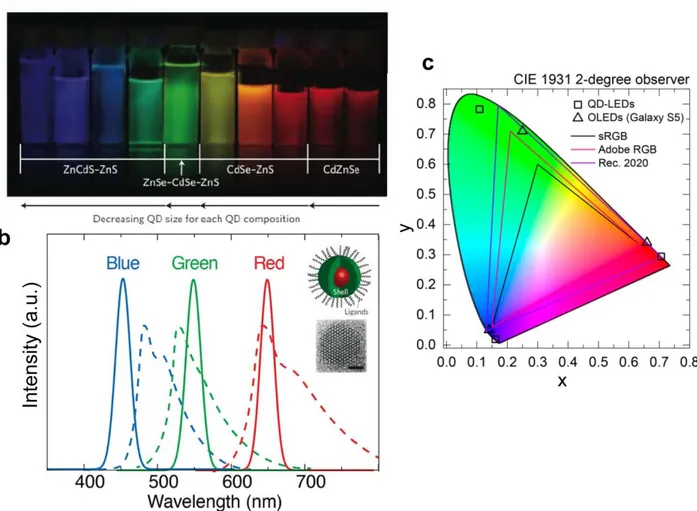
Figure 1-1: Historical evolution of LED and display technology. ... 21 Figure 2-1: Tunable and pure emission from colloidal QDs. (a) Photograph of colloidal QD
solutions of varying size and composition under ultraviolet excitation, exhibiting color tunability in the visible spectrum21. (b) Comparison of emission spectra of blue, green, and red QDs (solid lines) to organic dyes used in organic light-emitting diodes (OLEDs) at similar wavelengths (dashed lines). Adapted from ref. 24 Inset: schematic of a typical core-shell QD structure (top), and a high-resolution transmission electron microscope image of a CdSe QD, scale bar is 1.5nm (bottom). Adapted from Ref.25 (c) CIE 1931 diagram that highlights representative RGB color spaces (solid lines) and chromaticity points of RGB QD-LEDs (squares) and state-of-the-art Galaxy smartphones based on OLEDs (triangles). Adapted from ref. 26... 26
Figure 2-2: (a) PL images of RGB QD pixels fabricated using microcontact printing with
resolution of 441 ppi (left) to 2460 ppi (right). Adapted from ref.31 (b) Photograph of Inkjet-printed MIT seal pattern with QDs on glass at ONE Lab (Courtesy of Giovanni Azzellino). ... 27
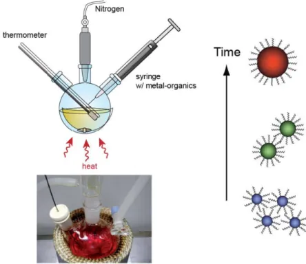
Figure 2-3: Schematics of colloidal QD synthesis setup. Adapted from ref. 49 ... 30
Figure 2-4: (a) Schematic of electronic band structures of nanocrystals from bulk to QDs with
decreasing size. Adapted from ref. 52 (b) Energy band diagram for direct gap semiconductor (left) and energy band diagram showing discrete optical transitions in finite size semiconductor nanocrystals due to quantum confinement (right). Adapted from ref. 51 ... 32
Figure 2-5: Schematic illustration of device structures and operation mechanism of (a) a
QD-LCD that uses QD photoluminescence (PL), and (b) a QD-LED that utilizes QD electroluminescence (EL). ... 34
Figure 2-6: (a) Color gamut comparison of commercial QD-LCD TV and regular LCD TVs with
respect to NTSC and Rec.2020 standard color space. Adapted from Ref. 58 (b) Photograph of Nanosys’ white LED demo using QD enhancement film containing red and green QD with blue
12
LED backlight. The exploded section shows red and green QDs patterned into 100 x 300 micron subpixels. Adapted from ref. 59 ... 35
Figure 2-7: (a) Schematic illustration of hybrid organic-inorganic QD-LED device architecture.
(b) Flat band energy level diagram of a typical hybrid QD-LED with ITO used as transparent electrode, highlighting the charge injection and exciton formation processes. ... 36
Figure 2-8: Progression of visible QD-LED device performance over time in terms of peak EQE.
Record performances are highlighted on the top right corner with star labels. Inset: QD-LEDs are classified into two types with device structures shown, as detailed in the text. Data points are taken from references9,10,21,48,68–89 ... 38
Figure 2-9: Schematic illustration of perovskite crystal structure. Adapted from ref. 107 ... 41
Figure 2-10: PL spectra of MAPbX3 (MA= methylammonium) perovskite thin films with
different halide compositions on (bottom) and images of corresponding perovskite film sample under a UV lamp (top). Adapted from ref. 114 ... 42
Figure 2-11: Schematic illustrations of (a) representative perovskite thin film deposition
methods via solution processing, and (b) typical colloidal perovskite QD synthesis methods. Adapted from ref. 116,121 ... 44
Figure 3-1: Schematic (top) of photo-excited QD thin film with an electric field applied across
the QD thin film, and pictures (bottom) illustrate electric field-induced exciton polarization and dissociation processes. ... 49
Figure 3-2: (a) Cross-sectional view of the capacitor device structure with QD sandwiched
between two dielectric layers. (b) PL spectra (top) of the QD film photoluminescence under excitation in ‘ON’ and ‘OFF’ state, and pictures (bottom) of the device in both states with black arrow indicating the operating pixel. ... 52
Figure 3-3: Steady state PL spectra of QD thin film optically excited with λ = 405 nm light. ... 53 Figure 3-4: (a) Normalized PL intensity under 40Vpp square-wave with 20V offset at frequency
13
Figure 3-5: Fractional QD PL quenching with respect to glass/QD reference sample as a
function of different sample structures. ... 56
Figure 3-6: (a) Schematic of QD-LED device architecture with cross-sectional TEM image of
the device stack prepared by focused ion beam showing each layer of the device. The QD thin film is excited λ = 405 nm light and the PL signal is recorded. (b) Illustration of the band diagram of the device under reverse bias. The applied electric field spatially separates the electron and hole wavefunctions of a QD exciton (indicted by the dashed line). ... 59
Figure 3-7: QD-LED (with 10 nm thick QD layer) performance under forward bias. Inset: photo
of device operated at 5V forming a MIT pattern. (a) current density-voltage-luminance characteristics (b) EQE versus current density. Inset: electroluminescence spectrum. ... 60
Figure 3-8: Current density-voltage characteristic of the device from -20 to 5V. ... 61 Figure 3-9: (a) Steady state PL spectra of a QD-LED with 10 nm thick QD film, optically
excited with λ = 405 nm light. Drop in PL intensity and a red shift in peak PL wavelength is observed with increasing reverse-biased electric field. The PL fully recovers after the field is removed. (b) Integrated PL intensity (normalized) as a function of applied electric field shows the maximum achievable quenching of 99.5% at 3.3 MV/cm. The corresponding reverse bias voltage is indicated in the plot. ... 62
Figure 3-10: CCD camera images of QD-LED (with 10 nm thick QD layer) under microscope
illuminated with a λ = 405 nm LED under (a) 0 V and b) -20 V and -24 V reverse bias. Illumination is masked outside of the octagonal iris. The faint rectangular shape in each sub-figure of (b) outlines the active region of the device. The residual luminance observed at -24 V is due to EL resulting from dielectric breakdown. ... 62
Figure 3-11: (a) Electroabsorption spectra of a monolayer thick QD film in a QD-LED under
reverse bias. (b) Integral of the electroabsorption spectrum from 1.77eV (λ = 700nm) to 2.70eV (λ = 460nm). ... 63
Figure 3-12: (a) Time traces of the device as a function of the applied electric field showing the
14
at the start (top) and the end (top) of a -10V pulse for a device with a 10 nm thick QD layer. The fast response time and recovery time are on the order of three hundred nanoseconds. ... 64
Figure 3-13: Time-resolved PL decays of a QD-LED with 10 nm thick QD layer reverse biased
with increasing electric field from 0 to 1.7 MV/cm. Inset: normalized decay traces. The samples are excited using a λ = 405 nm pulsed laser. ... 66
Figure 3-14: Integrated PL intensity (normalized) of the device as a function of the excitation
wavelength (from λ= 460 nm to λ = 560 nm) with increasing applied electric field. ... 67
Figure 3-15: (a) PL spectrum fit for a device with 10 nm thick QD layer is shown in a) under no
field, and (b) under the field of 1.7 MV/cm. The raw spectrum data, model fit, and the two Voigt fit functions are shown in black, green, red, and blue, respectively. The peak wavelength and intensity fraction of the two peaks are plotted as a function of field from 0 to 1.7MV/cm in (b) and (c). ... 69
Figure 3-16: (Top) PL intensity and peak PL wavelength measured across two reverse bias
pulses of VON=-10 V with durations of 6 s and 14 s, separated by 100 s of zero bias. The small
spikes correspond to scattered light from lasers used in differential absorption measurements, which are taken simultaneously. The device measured has a 30 nm thick layer of quantum dot film. (Bottom) Change in electron occupancy and e-field on the QD film compared to time t=0, as extracted from differential absorption spectra. Each point derives from a spectrum acquired over 2 seconds. ... 73
Figure 3-17: Absorption (blue line) and PL (red line) spectra of the red CdSe-ZnCdS QDs used
in the device. Inset: TEM image of QDs. Scale bar is 10 nm. ... 76
Figure 3-18: SEM images of a monolayer of QD film. Scale bar is 100 nm (left) and 1 um (right)
... 76
Figure 4-1: (a) Energy level diagram showing the band-edge energies of bulk CdSe, InP, ZnSe
and ZnS. (b) Illustration of spectrum coverage of Cd-based QDs that cover visible (CdSe and CdTe), ultraviolet (CdS) and infrared (PbS and PbSe) regions, compared with Cd-free
15
alternatives that cover visible (InP, CuInS2 and Si), ultraviolet (ZnSe) and infrared (InAs)
regions. Adapted from ref. 26 ... 81
Figure 4-2: Schematic illustrates of the synthesis of ZnSe seed core, ZnSe core and ZnSe/ZnS
QDs via continuous-injection, with corresponding TEM images. Courtesy of Jason Yoo. ... 84
Figure 4-3: Optical properties of blue QDs. Absorption and PL Spectra before (a) and after (b)
adding Zn and S precursor for shell growth. (c) PL emission peak and FWHM as a function as reaction time. (d) Solution PL quantum yield (PLQY) as a function of shell growth time. Inset: photograph taken of QD solution under illumination at 365 nm. Courtesy of Jason Yoo. ... 86
Figure 4-4: (a) PL spectrum of blue QD thin film on glass substrate. Inset: photograph of blue
QD excited under UV light. (b) AFM topography (top) and phase (bottom) scans of the surface of the QD film. ... 88
Figure 4-5: (a) Schematic of the blue QD-LED device architecture. (b) Energy-band diagram of
the QD-LED. ... 89
Figure 4-6: Performance of the blue QD-LED. (a) Voltage-dependent current density (J-V). (b)
Voltage dependence of the (EQE-V). (c) Voltage-dependent luminance (L-V) (d) Electroluminescence (EL) spectrum of the device operated at 6V. Inset: photograph of the operating device. ... 90
Figure 5-1: (a) Schematics of dual-source vacuum deposition of perovskite thin film. (b) XRD
spectra and c) SEM images of deposited CsPbBr3 film with varying CsBr: PbBr2 ratios (1:1 to
5:1). The scale bar is 500 nm. ... 96
Figure 5-2: Optical properties of vapor-deposited CsPbBr3 films with varying precursor ratios.
(a) Absorption spectra (b) Photoluminescence (PL) spectra (inset: photograph of perovskite films excited under a UV lamp). ... 98
Figure 5-3: a) Schematic of device architecture of the all-vapor-deposited perovskite LEDs. (b)
Flat band diagram of all functional layers, with energy levels shown for TCTA, CsPbBr3, and
TPBi. Band energies are obtained from literature209,210, and are expressed in eV (all referenced to the vacuum level). ... 99
16
Figure 5-4: Performance of vapor-deposited CsPbBr3 perovskite LEDs with different precursor
ratios. (a) Current density-voltage-luminance (J-V-L) characteristics. (b) EQE-voltage characteristics. (c) Statistics of peak EQE of ten devices for each precursor ratio. The red mark in each box represents the median value, and the top and bottom edges of the box indicate the 25th and 75th percentiles, respectively. The error bars represent the maximum and minimum values. (d) Electroluminescence spectrum of the best performing device with 5:1 precursor ratio. Inset: photo of one of the ten devices on a substrate being operated at an applied bias of 5.5V. ... 101
Figure 6-1: Potential architecture of QD photoluminescence display with patterned red, green
and blue PLP216. ... 107
Figure 6-2: Summary of peak EQE as a function of T50 lifetime of representative red, green and
blue QD-LEDs (Cd-based devices in open squares and Cd-free devices in solid squares) and state-of-the-art OLEDs (with fluorescent, phosphorescent and TADF devices in open circles, solid circles and solid triangles, respectively), all compared at the same initial luminance of 1000 cdm-2 (nits). All devices are tested under ambient conditions with glass encapsulation. The grey dashed line highlights the 10,000 hours lifetime requirement for realistic display applications. Data points are taken from ref. 218–234 ... 109
18
List of Tables
Table 2-1: Performance summary of red, green and blue QD-LEDs and phosphorescent OLEDs
... 39
Table 2-2: Performance summary of highly efficient perovskite LEDs. (MA = methylammonium
and BA = butylammonium) ... 46
Table 3-1: Summary of previously reported voltage-controlled photoluminescence quenching of
QD ensembles ... 50
Table 3-2: Decay lifetimes as a function of applied electric field ... 66 Table 5-1: Device performance of all vapor-deposited CsPbBr3 based perovskite LEDs with
20
Chapter 1 Introduction
1.1 Evolution of LED and display technology
Ever since the beginning of the color display era, it has been people’s dream to create electronic devices that can accurately produce the colors of our natural world, giving viewers the best visual experience. It is safe to say that the birth of LEDs and displays highlighted the beginning of a new world where we have turned our imagination into reality. People use displays all the time – at work (laptop and desktop monitors), at home (TVs), and on the go (smartphones, tablets, and wearable devices). When I was writing this thesis at home because of the global pandemic, I was constantly reminded of the profound impact that display technology has had on my life. It has become an indispensable part of the modern world and has shaped our lifestyle tremendously.
Since the invention of the incandescent light bulb back in the 19th century, the evolution of electronic display technology has been continuously driven by the development of new materials and novel device concepts. Figure 1-1 gives an overview of display technology evolution over the years, from the power-hungry and ugly displays of the 1900s to the colorful, slim, and energy-efficient displays of today, highlighting the key material and device innovations. Right after the light bulb was invented, cathode ray tube (CRT) was introduced with the first TV made in the 1930s, which used electron guns in a vacuum tube to display images on a phosphorescent screen1. While CRT technology was incredibly robust for a long time, it was eventually replaced by plasma and liquid crystal displays (LCDs) because of its bulkiness and energy inefficiency. LCD is a non-emissive display technology that uses liquid crystals to
21
manipulate the backlight traveling through2. Thin-film transistor (TFT) LCD technology has undergone decades of material and device innovation to finally become mature3.
Figure 1-1: Historical evolution of LED and display technology.
One important milestone to note was the invention of red light emitting diodes (LEDs) back in 1960, followed by the discovery of efficient blue LEDs, which later won the 2014 Nobel Prize in Physics4. The birth of LED technology not only allowed us to enter the modern display era but also transformed our everyday light sources replacing incandescent light bulbs. LCDs with LEDs used as the backlighting unit brought us flat-panel and portable display products that people could not even imagine before. In the past 30 years, a new class of semiconductor materials has emerged, expanding the existing light emitting materials to an even larger library of organic molecules, polymers, and colloidal nanocrystals. These new materials possess unique electrical and optical characteristics, including superior color performance and luminescence efficiency. LEDs based on these materials could potentially enable even lighter, thinner, bright, and more energy-efficient displays with new form factors (e.g. foldable and flexible). Since
22
organic light emitting diode (OLED) was invented back in 19875, thin-film LED technology has truly transformed emissive displays and become a competitive alternative to LCDs. Today, OLED technology is everywhere. It is adopted in almost all major flagship smartphones and the technology has established a multi-billion-dollar display market6. This is largely because of OLED’s lower energy consumption, higher contrast ratio, wider viewing angles, and compatibility with high-resolution patterning compared to LCDs. However, challenges associated with the long-term stability of organic materials and the cost of large-area manufacturing have limited OLED’s competitiveness to small-sized displays to this date.
In the search for low cost, large area, and high color-quality displays, thin-film LED based on nanostructured materials, such as colloidal quantum dots (QDs) and lead halide perovskites, emerged after OLED in recent years. Thanks to the advances in colloidal synthesis over the past several decades, colloidal nanocrystals or quantum dots (QDs) have been utilized in various optoelectronic devices, including solar cells7,8, LEDs9,10, and photodetectors11. The QD material market has recently been reported to be worth $2.6 billion in 2018, and the market is projected to be valued at $8.5 billion by 2023 with a daunting annual growth rate of 27%12. Lead halide perovskites, on the other hand, have shown great promise in both solar and LED devices as the efficiency of perovskite solar cell13 and LED14 both reached >20% in just a short period.
23
1.2 Thesis organization
This thesis will examine the use of visible colloidal nanocrystal QDs and lead halide perovskites as luminophores in both optically- and electrically-driven thin-film light emitting devices. Chapter 2 will provide background knowledge of colloidal QDs and lead halide perovskites. It covers their basic material properties, advantages they bring as light emitters, as well as fundamentals of QD- and perovskite-based LEDs. In Chapter 3, we explore two ways of actively modulating CdSe QD thin film photoluminescence (PL) using an external electric field. We first study field-induced PL modulation in a QD capacitor structure, and then we report a novel way of operating a QD-LED that exhibits reversible, fast and near-complete quenching of the PL of QD thin film that has a high zero-field PL quantum yield. Chapter 4 discusses the development of heavy-metal-free blue QD-LEDs. We demonstrate a synthesis of high-quality ZnSe-ZnS core-shell QDs, and QD-LEDs with efficient, clean, and narrow violet-blue electroluminescence (EL). In Chapter 5, we will focus on the deposition of CsPbBr3 perovskite thin films by thermal
co-evaporation, demonstrating an all vacuum-processed perovskite LED device. Finally, Chapter 6 presents a summary of this thesis and an outlook for QD- and perovskite-based light emitting technologies.
24
Chapter 2 Background
2.1 Colloidal Quantum dot as Luminophores
In this section, we present the fundamentals of colloidal quantum dots (QDs). First, we discuss the benefits of adopting QDs as light emitting materials. Next, we give a brief introduction to colloidal QD synthesis and cover its electronic and optical properties. Finally, QD based light emitting devices are introduced, focusing on the two ways of exciting QD, basic device operating principles, and device performance progress over the years.
2.1.1 Advantages of QDs for display applications
Colloidal quantum dots (QDs) are solution-processed nanocrystal semiconductor materials. As shown in Figure 2-1b inset, these materials typically consist of a small inorganic semiconductor core (1-10 nm in size), a larger bandgap inorganic semiconductor shell, and organic passivating ligands surrounding the shell surface. These nanocrystals emit saturated, bright, and tunable colors of light, making them especially attractive for display and lighting applications15. One of the greatest characteristics of QDs is their size-tunable emission. Since QDs are nanometers in size, their energy level structure is therefore determined by the quantum confinement effect instead of inherent bulk properties16. The detailed quantum mechanical derivation of this bandgap tunability can be found in several other studies17,18, and is briefly discussed in section 2.1.3. The electron-hole pair formed by excitation interacts via coulomb attraction to form an exciton. The exciton is characterized by the binding energy and an exciton Bohr radius, which is derived similarly to the Bohr model of a hydrogen atom. The confinement of excitons, which is on the order of bulk Bohr exciton radius, leads to the quantization of bulk energy levels, resulting
25
in size-tunable bandgap19. That is, the smaller the nanocrystal, the higher energy of the emission. This is illustrated in Figure 2-1a, which demonstrates how this spectral tunability can also be extended to cover the entire visible spectrum by modifying QD chemical stoichiometries and compositions20,21. In addition to its tunable color, QD's emission also possesses high color purity, which can be quantified by comparing the spectra full-width half-maximum (FWHM) of the emitter. As shown in Figure 2-1b, CdSe-based QDs, which cover the visible spectrum, typically have FWHM ~30 nm or less22, much narrower compared with traditional inorganic phosphors and organic dyes (FWHM ~50-100 nm)23, making QDs as outstanding light emitters with saturated color. Color purity is crucial when it comes to color gamut for display technologies.
Figure 2-1c shows a Commission International del Eclairage (CIE) chromaticity diagram. In
displays, images are generated by sub-pixels that are red, green, and blue (RGB), and each is actively controlled. The CIE diagram maps color in terms of saturation and hue, and the boundary of the color map defines the different saturated hues that the human eye can detect. The area enclosed by the black open squares is the color gamut achievable using RGB QDs, and it exhibits a much larger color gamut than the area formed by state-of-the-art OLEDs (open triangles) used in today’s Galaxy smartphones. The diagram also highlights several standard color spaces and we can see that while OLEDs can only cover sRGB or Adobe RGB, QDs easily exceed the current standards and match up to Rec.2020, which is the recommended color space for next-generation displays capable of delivering 4K or 8K ultra-high-definition images.
26
Figure 2-1: Tunable and pure emission from colloidal QDs. (a) Photograph of colloidal QD
solutions of varying size and composition under ultraviolet excitation, exhibiting color tunability in the visible spectrum21. (b) Comparison of emission spectra of blue, green, and red QDs (solid lines) to organic dyes used in organic light-emitting diodes (OLEDs) at similar wavelengths (dashed lines). Adapted from ref. 24 Inset: schematic of a typical core-shell QD structure (top), and a high-resolution transmission electron microscope image of a CdSe QD, scale bar is 1.5nm (bottom). Adapted from Ref.25 (c) CIE 1931 diagram that highlights representative RGB color spaces (solid lines) and chromaticity points of RGB QD-LEDs (squares) and state-of-the-art Galaxy smartphones based on OLEDs (triangles). Adapted from ref. 26
27
By overcoating the core material with a wider bandgap inorganic semiconductor shell, the photoluminescence quantum yield (PLQY) and photostabilities of QDs can be dramatically improved. This is mainly because the outer shell help passivates the surface dangling bonds, which usually serve as non-radiative recombination sites, and confine excitons to the semiconducting core27,28. For instance, by utilizing a CdSe-CdS core-shell structure, the resulting nanocrystals exhibit a solution PLQY as high as 100%, which is almost an order of magnitude higher compared to that of a naked CdSe core29. Moreover, it has been demonstrated that the photostability of QDs exceeds that of many inorganic phosphors and organic dyes, therefore offering an advantage for their implementation in displays under optical excitation (discussed later). By combining a thick inorganic multi-shelled structure with surface passivating ligands, QDs of intrinsic PL lifetime of over 10,000 hours have been demonstrated30.
Figure 2-2: (a) PL images of RGB QD pixels fabricated using microcontact printing with
resolution of 441 ppi (left) to 2460 ppi (right). Adapted from ref.31 (b) Photograph of Inkjet-printed MIT seal pattern with QDs on glass at ONE Lab (Courtesy of Giovanni Azzellino).
Moreover, via modifying its surface ligands, QD can dissolve in a variety of organic solvents. Solution-processed QDs offer the advantage of using low-cost and large-area deposition techniques such as microcontact printing32 and inkjet printing33. Choi et al.31
28
demonstrated a QD pixel line width of <1 um and a high patterning resolution of 2460 ppi by using intaglio transfer printing (Figure 2-2a). They were able to achieve transfer yield as high as 100% regardless of the size or shape of the patterns. While this and many other studies34,35 have proven that high-resolution patterning of QD films can be obtained by transfer printing, numerous challenges still remain, including particle contamination during the printing process and detachments of QD sub-pixels. Furthermore, the large-scale inkjet printing process is currently under active development in the display industry. For example, Kateeva Inc., the leader in this area, has demonstrated mass production lines based on inkjet printing that is capable of handling G8-size glass substrates36, which is the standard for fabricating over 55-inch flat-panels. More recently, one of the leading OLED TV manufacturers, JOLED Inc., showcased their 19.3
inch 4K OLED display panels37. Last year, the Chinese TV panel manufacturer BOE
demonstrated the world’s first inkjet-printed 55 inch OLED TVs38. One major challenge of inkjet printing is to avoid the well-known coffee-ring effects, which can result in solute particles at the rim of a dried liquid droplet, causing thin film non-uniformity39. Jabbour et al pioneered the fabrication of QD displays using inkjet-printed pixelated arrays of QD thin films33. Figure 2-2b shows an example of inkjet-printed QD film with a MIT seal pattern at our Lab.
29
2.1.2 Colloidal QD synthesis
Researchers have made tremendous advances on nanocrystal synthesis, and numerous review papers address this topic in excellent detail40–42. Here we only aim to give a brief introduction. QDs are usually categorized by their synthetic route into two types - colloidal and epitaxial (or known as self-assembled). Compared to epitaxial QDs, which often require ultrahigh-vacuum environments for growth43, colloidal QDs can be prepared by ‘wet’ chemical synthesis methods that enable superior size and shape control, as well as higher spectral purity, monodispersity, and photoluminescence intensity44. It is also noted that the relatively facile and inexpensive solution-based synthesis of colloidal QDs has a superior impurity tolerance compared to that of epitaxial growth. In addition, people only observe a weak confinement effect in epitaxial QDs45 due to their relatively large lateral dimensions and the difficulties to control their size. In contrast, colloidal QDs offer simple size tunability of emission. Unlike epitaxial QDs that are bound by the substrates, colloidal QDs are amenable to thin-film assembly and chemical processing steps46.
In order to be adopted for display applications, high-quality QDs are characterized by a well-defined and controlled size, with a narrow size distribution to achieve the stringent color emission requirements of displays. Bawendi et al.47 pioneered the hot-injection method that uses a three-neck flask (Figure 2-3) for the synthesis of high quality and monodisperse colloidal nanocrystals (minimal size variation). This benchmark preparation method22 involves a rapid injection of organometallic precursors into hot organic solvents at temperatures around 300 °C. Thermally activated nucleation and growth of small crystallites from the precursors slowly occur until arrested by cooling. The size and consequently the emission wavelength are determined by the growth time and reaction temperature and are monitored throughout the synthesis process by measuring absorption spectra of aliquots extracted from the growth solution. Overcoating QD
30
core material with shell and organic ligands ensures good surface passivation and solubility in common solvents. Prior to film deposition, QDs are often precipitated and redissolved several times to get rid of excess ligands (detailed in Appendix A), and then recast in the desired solvent for following solution-based deposition48.
31
2.1.3 Electronic and optical properties of QDs
The size-tunable color of colloidal QDs is their most unique and interesting property. Although modifications to QD structures over the years make their physical properties to be complex, their bandgap tunability is fundamentally governed by the quantum confinement effect19,50,51. By definition, the Bohr radius of a bulk exciton is given by,
𝑎𝑎𝐵𝐵 = ħ
2𝜅𝜅
𝜇𝜇𝑒𝑒2
(2-1)
where 𝜅𝜅 is the dielectric constant of the semiconductor and 𝜇𝜇 is the reduced mass of the electron-hole pair. When the QD radius is smaller than the material’s Bohr radius, the energy levels of a QD exciton can be approximated by considering the QD as a particle-in-sphere problem with infinite potential walls (Figure 2-4a). As a result, only certain states that satisfy the boundary conditions are allowed, shown in Figure 2-4b, and this leads to the quantization of bulk energy levels and atomic emission-like spectra50. The confinement energy is given by,
𝐸𝐸𝑙𝑙,𝑛𝑛𝑒𝑒,ℎ = ħ2𝜙𝜙𝑙𝑙,𝑛𝑛2
2𝑎𝑎2𝑚𝑚𝑒𝑒,ℎ
(2-2)
where 𝜙𝜙𝑙𝑙,𝑛𝑛 is the nth root of the spherical Bessel function of order 𝑙𝑙, and 𝑚𝑚𝑒𝑒,ℎ is the effective mass of the electron or hole. We can then apply the effective mass approximation, modeling the conduction and valance bands as parabolic. The particle wavefunctions can be described as linear combinations of Bloch functions. The QD exciton energy is then given by,
𝐸𝐸𝑒𝑒𝑒𝑒𝑒𝑒𝑒𝑒𝑒𝑒𝑒𝑒𝑛𝑛 = 𝐸𝐸𝑔𝑔+ ħ 2 2𝑎𝑎2� 𝛽𝛽𝑛𝑛𝑒𝑒𝑙𝑙𝑒𝑒2 𝑚𝑚𝑒𝑒 + 𝛽𝛽𝑛𝑛ℎ𝑙𝑙ℎ2 𝑚𝑚ℎ � − 1.8𝑒𝑒2 4𝜋𝜋𝜋𝜋𝑎𝑎
(2-3)
where the first term 𝐸𝐸𝑔𝑔 is the bulk bandgap of the semiconductor. The two middle terms are accounting for the quantum confinement energies of electrons and holes. They are dependent on the size of the QD: as QD gets smaller, its confinement becomes stronger, the exciton energy increases, and we will see a higher energy (bluer) photon emission. The final term describes the
32
first order Coulombic attraction between the electron and hole. The 1.8 factor come from the fact that we assume the electron and hole are both in their respective lowest excited state, i.e. 1S state. In the case of CdSe, the bulk bandgap of this material is 1.73 eV, but the bandgap energy of CdSe QDs can be tuned by its size to as high as 2.8 eV.
Figure 2-4: (a) Schematic of electronic band structures of nanocrystals from bulk to QDs with
decreasing size. Adapted from ref. 52 (b) Energy band diagram for direct gap semiconductor (left) and energy band diagram showing discrete optical transitions in finite size semiconductor nanocrystals due to quantum confinement (right). Adapted from ref. 51
The quantum confinement effect derived from the simple parabolic band approximation allows us to relate QD size with PL energy. However, it is worth emphasizing that a more detailed multi-band effective mass approximation is required to describe some of the complexities of a QD PL spectrum. We need to note that the band-edge exciton state is eight-fold degenerate, that is, a product of two-fold degenerate electron states and four-fold degenerate hole states. This can complicate the absorption peak (Stock shift) and radiative lifetimes of QDs (an order of magnitude longer than the bulk counterpart)53. These can be attributed to the fact that the lowest energy exciton state is a “Dark Exciton” state, which is optically inactive and sits at
33
lower energy than an optically active “Bright Exciton” state53. Interestingly, these two states are less than 𝑘𝑘𝑏𝑏𝑇𝑇 apart, making QDs efficient at room temperature.
34
2.1.4 Quantum dot light emitting devices
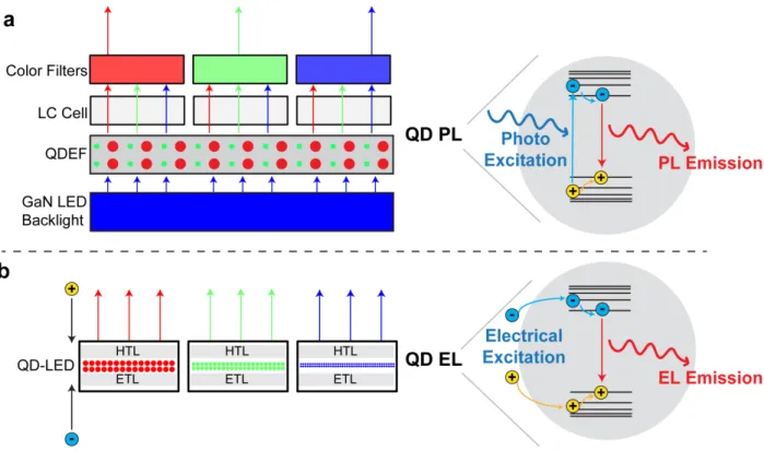
The amazing luminescent properties of colloidal nanocrystals have stimulated commercial applications of QDs in the display industry. As QDs can be either optically or electrically excited, the resulting emissions are categorized into photoluminescence (PL) and electroluminescence (EL). Figure 2-5a gives a schematic illustration of QD optical excitation, where an exciton is formed in a QD by absorbing a higher energy photon. QDs can also be excited electrically (Figure 2-5b), forming an exciton through injecting charge carriers directly into the QD using charge transport layers (CTLs).
Figure 2-5: Schematic illustration of device structures and operation mechanism of (a) a
QD-LCD that uses QD photoluminescence (PL), and (b) a QD-LED that utilizes QD electroluminescence (EL).
QD materials have already been successfully commercialized to replace conventional inorganic phosphors in liquid crystal displays (LCDs). Today, red and green QDs are used as optical down-converters for the blue LEDs back-light to generated white light54,55. This technology is known as Quantum Dot Enhancement Film (QDEF). Several companies in the display industry, including Samsung, TCL, Sony, BOE, TCL, and others, have introduced a number of QD-enhanced LCD TVs to their product line over the past few years. LCDs that use
35
conventional phosphors as down-converters can achieve only 70% of the color gamut of the NTSC (National Television System Committee) standards56. By utilizing QDEF technology with saturated colors inherited from QD’s narrow PL emission, the color gamut is drastically improved to more than 110% of the NTSC standard57, enabling LCD displays with more vivid colors (Figure 2-6a) without drastically increasing the panel cost. Figure 2-5a depicts a schematic illustration of LCD with QD down-converter films incorporated and placed in front of the blue LED back-light. An example of such QD color down-conversion is demonstrated in Figure 2-6b, where QD enhancement film containing red and green QD are patterned and placed in front of a blue LED backlight to generate a bright white light.
Figure 2-6: (a) Color gamut comparison of commercial QD-LCD TV and regular LCD TVs with
respect to NTSC and Rec.2020 standard color space. Adapted from Ref. 58 (b) Photograph of Nanosys’ white LED demo using QD enhancement film containing red and green QD with blue LED backlight. The exploded section shows red and green QDs patterned into 100 x 300 micron subpixels. Adapted from ref. 59
Besides using QDs as a color enhancement film, electrically driven quantum dot light-emitting diodes (QD-LEDs) are seen as the ultimate display technology. QD-LEDs are self-emitting devices that do not require LED back-light (Figure 2-5b). The light emission of QD-LEDs is driven by the current flows to each sub-pixel, which is controlled by thin-film transistor (TFT) backplanes60. Because of their self-emitting feature, QD-LED shares many advantages
36
similar to the current state-of-the-art OLED technology, including higher contrast, faster response time, and wider view angle. But compared to OLED displays, the superior properties of QDs as emissive materials also offer distinct advantages for QD-LED displays.
Figure 2-7: (a) Schematic illustration of hybrid organic-inorganic QD-LED device architecture.
(b) Flat band energy level diagram of a typical hybrid QD-LED with ITO used as transparent electrode, highlighting the charge injection and exciton formation processes.
As mentioned earlier, one feature of QDs is their super narrow emission, which results in even more color-saturated emission than organic dyes. While color filters are essential in an OLED display, which unavoidably causes energy loss61, electrically driven QD display could potentially eliminate the use of color filters62. More importantly, OLED stability, especially blue devices, is one of the most well-known roadblocks currently limiting the performance of this technology63,64. Even after nearly two decades of research and development, the lifetime of blue OLEDs still remains much inferior compared to their red and green counterparts65. QDs with a core-shell structure exhibiting superior intrinsic photo- and thermal-stability compared to organic materials are promised to overcome this lifetime hurdle.
37
Figure 2-7a depicts a typical QD-LED device architecture, which typically has a p-i-n
structure, comprising two electrodes that under forward bias, inject opposite charges into a series of charge injection and transport layers sandwiched in between. As illustrated in the energy level diagram in Figure 2-7b, the injected electrons and holes meet in the QD emitting layer to form excitons, which can then radiatively recombine to emit light. QD-LEDs have evolved significantly since their initial demonstration in 199466. In the past two decades, their external quantum efficiency (EQE) has increased from less than 0.01% to more than 20%, catching up to the state of the art OLEDs67. EQE measures the number of photons emitted by the LED in the viewing direction to the number of electrons injected and it is expressed as:
𝐸𝐸𝐸𝐸𝐸𝐸 = 𝜂𝜂𝑟𝑟× 𝜂𝜂𝑃𝑃𝑃𝑃× 𝜂𝜂𝑒𝑒𝑜𝑜𝑒𝑒 (2-4)
where 𝜂𝜂𝑟𝑟 is the ratio of is the ratio of excitons generated to the electron injected, 𝜂𝜂𝑃𝑃𝑃𝑃 is the photoluminescent quantum yield (PLQY) of the QDs, that is, the ratio of photons absorbed to photons emitted through fluorescence, and 𝜂𝜂𝑒𝑒𝑜𝑜𝑒𝑒 is the fraction of emitted photons that are coupled out of the devices. The general challenge to achieving high efficiency in QD-LEDs is the simultaneous optimization of all three factors.
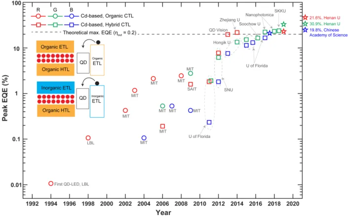
Figure 2-8 summarizes the progress of device performance of visible QD-LEDs over the
years in terms of peak EQE, as EQE is directly proportional to power conversion efficiency, which is a key metric when it comes to displays. Modern QD-LED device architectures can be divided into two categories. Devices demonstrated in the early years were a natural progression from polymer and organic LEDs, and as a result, QDs were typically sandwiched between two organic charge transport layers, depicted in the inset of Figure 2-8. QD EL was readily achieved, yet EQEs remained low (<10%), largely because of the low
𝜂𝜂
𝑃𝑃𝑃𝑃of QDs at the time. The efficiency was also limited by the limited brightness as a consequence of very low current38
densities reachable using QDs together with organic semiconductors as charge injection and transport materials.
Figure 2-8: Progression of visible QD-LED device performance over time in terms of peak EQE.
Record performances are highlighted on the top right corner with star labels. Inset: QD-LEDs are classified into two types with device structures shown, as detailed in the text. Data points are taken from references9,10,21,48,68–89
In early 2009, a new hybrid structure was introduced, comprising an inorganic metal oxide electron transport layer (notably solution-processed ZnO nanoparticles) and an organic semiconductor hole transport layer72,73. This revolution in device architecture resulted in significant efficiency gains with QD-LEDs. Devices with EQE as high as 20% started to emerge48, reaching the outcoupling ceiling of ~20-25%90 and making them competitive with those commercially mature phosphorescent OLEDs91. ZnO nanoparticles offer improved electron injection compared with organics without introducing interfacial intricacies that damage
𝜂𝜂
𝑃𝑃𝑃𝑃of39
QDs. Table 2-1 summarizes the record performance of QD-LEDs reported up to date and compares it to phosphorescent OLEDs. While QD-LED device efficiency still has room for improvements considering the potential photon outcoupling schemes that can be adopted92, they have a clear advantage in regard to emission color purity, reflected by the narrower spectral linewidth. Device lifetime T50, which is defined as the time taken for the initial brightness (100
cd m-2) of the emission to drop to half, is also included in the table. For both OLED and QD-LED, although the lifetimes of the red and green devices are well above the standards required for display applications93, the lifetime of the blue device is orders of magnitude shorter. A systematic study of device stability is expected to be an active area of research to be pursued in the coming years before the commercialization of QD-EL is viable.
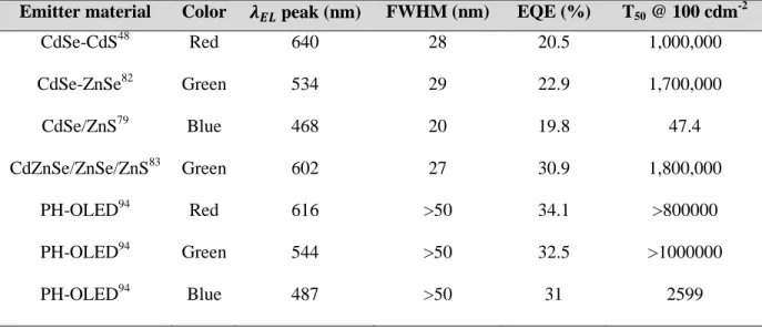
Table 2-1: Performance summary of red, green and blue QD-LEDs and phosphorescent OLEDs Emitter material Color 𝝀𝝀𝑬𝑬𝑬𝑬 peak (nm) FWHM (nm) EQE (%) T50 @ 100 cdm
-2 CdSe-CdS48 Red 640 28 20.5 1,000,000 CdSe-ZnSe82 Green 534 29 22.9 1,700,000 CdSe/ZnS79 Blue 468 20 19.8 47.4 CdZnSe/ZnSe/ZnS83 Green 602 27 30.9 1,800,000 PH-OLED94 Red 616 >50 34.1 >800000 PH-OLED94 Green 544 >50 32.5 >1000000 PH-OLED94 Blue 487 >50 31 2599
40
2.2 Metal halide perovskite as luminophores
In addition to colloidal QDs, metal halide perovskites are emerging as a new class of luminophores, which has driven intense research and development of perovskite light emitting devices for display and lighting applications in recent years. In this section, we offer a brief overview of metal halide perovskite semiconductors, their unique advantages as light emitters, and the fundamentals of perovskite light emitting devices.
2.2.1 Advantages of perovskites as light emitters
Metal halide perovskites are a class of semiconducting materials with an ABX3 chemical formula
and a crystal structure shown in Figure 2-9, where X represents a halide anion (Cl-, Br-, or I-), B represents a divalent metal cation (e.g. Pb2+ or Sn2+), and A is a monovalent cation (e.g Ch3NH3+). The 3D crystal structure maintains electroneutrality through having a series of
corner-sharing BX6 octahedral with “A” site cations sitting at the cubo-octahedral positions. Perovskites
are promising semiconducting materials for thin-film optoelectronics95–97 because they possess unique electro-optical properties, such as long carrier diffusion length98,99, high absorption coefficients100, and high tolerance to defects101. When used as photoactive films, perovskite solar cells with >20% power conversion efficiency have been demonstrated102. Perovskites have also shown great potential as light emitters as they exhibit narrow emission linewidth103, wavelength tunability across the visible spectrum104,105, and high photoluminescence quantum yields (PLQY)106. These photophysical traits make them attractive alternatives to organic dyes and colloidal QD luminophores for display and light applications.
41
Figure 2-9: Schematic illustration of perovskite crystal structure. Adapted from ref. 107
In lead-based perovskites, bandgap tunability is made possible by changing the stoichiometry of the halides at “X” site (Figure 2-10), enabling full visible spectrum coverage108. The emission color can be further extended to the infrared region by changing Pb (“B” site) with other metals like Sn. Moreover, 3D perovskites can be reduced to Ruddlesden-Popper phases109, commonly referred as quasi 2D perovskites, by introducing bulky organic cations at “A” site. This allows the emission color to be further tuned to cover the blue and violet regions. In addition to spectral tunability, perovskites also have a narrow emission linewidth, which is vital for display applications. Typical spectral widths of 20 nm for green110 and 35-40 nm for red have been reported111,112. Yet unlike colloidal QDs, perovskite emitters do not require a narrow particle size distribution in order to achieve saturated emission. Another distinct feature of perovskites is their facile and low-cost synthesis and fabrication. Lead halide perovskites can easily be synthesized and processed into thin films at room temperatures, which enables large-area deposition on different substrates including glass and flexible plastics113.
42
Figure 2-10: PL spectra of MAPbX3 (MA= methylammonium) perovskite thin films with
different halide compositions on (bottom) and images of corresponding perovskite film sample under a UV lamp (top). Adapted from ref. 114
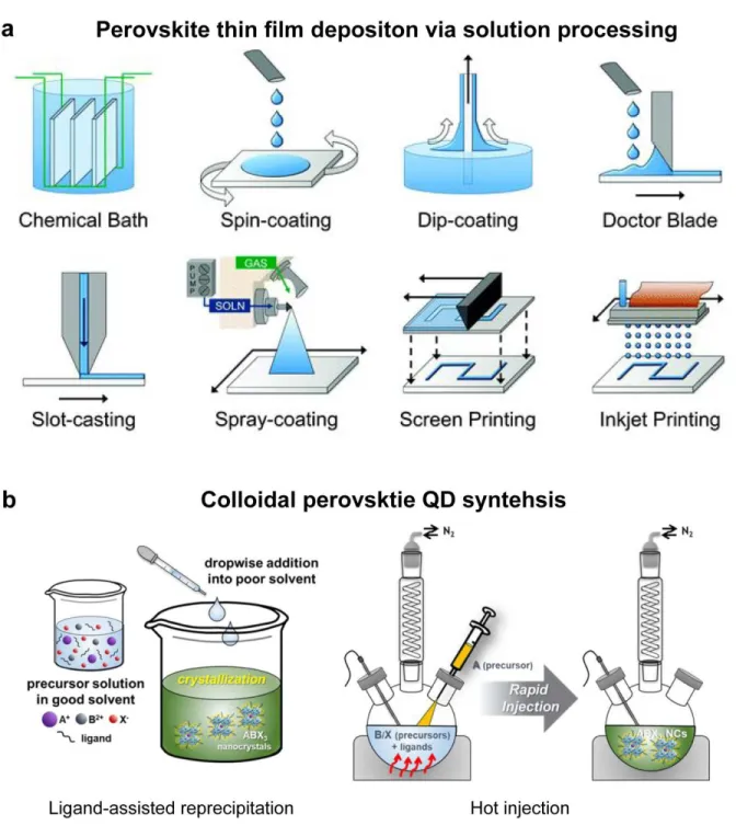
There are two main categories of perovskite when it comes to material synthesis: colloidal perovskite nanocrystals (QDs) and polycrystalline perovskite thin films. Figure 2-11 presents commonly used methods to synthesize perovskite QDs and deposit perovskite thin films via solution processing. Hot injection synthesis of perovskite QDs115,116 (Figure 2-11b left) is very similar to the procedures for Cd-based colloidal QDs described in section 2.1.2. Perovskite precursors (e.g. lead halide and organic halide salts) dissolved in nonpolar solvents are first headed to 150-200 °C, followed by injection of halide precursors to start nucleation and growth of nanocrystals. In addition to traditional hot injection, colloidal perovskite QDs can be obtained by reprecipitation synthesis (Figure 2-11b right)117–119. During a typical ligand-assisted reprecipitation, perovskite precursor materials are dissolved in polar solvents first. Nonpolar solvents are then added to the solution in the presence of surfactants. The difference in solubility between polar and nonpolar solvents initiates the recrystallization of perovskite nanocrystals and the ligands in solution prohibit the nanocrystals to aggregate to bulk forms. Unlike hot injection
43
which requires precise temperature control and an air-free environment, ligand-assisted reprecipitation can be performed at room temperature in the air. One major drawback of the reprecipitation method is the requirement of using polar solvents, which can often decompose the formed perovskite nanocrystals. Due to its success in producing high quality Cd-based colloidal QDs, hot injection is currently heavily adopted to synthesize perovskite QDs because it offers more effective control over the size of the nanocrystals120. To deposit polycrystalline perovskite film, people have explored various solution deposition techniques (Figure 2-11a) including but not limited to chemical bath, spin-coating, dip-coating, doctor blade coating, slot-casting, spray-coating, screen printing and inject printing121. Scalable alternatives that are solvent-free include vapor transfer deposition, flash evaporation, and thermal evaporation122,123, which will be the focus of Chapter 5. As will be discussed later, having a uniform and pinhole-free perovskite thin films are vital for high performance perovskite optoelectronic devices.
44
Figure 2-11: Schematic illustrations of (a) representative perovskite thin film deposition
methods via solution processing, and (b) typical colloidal perovskite QD synthesis methods. Adapted from ref. 116,121
45
2.2.2 Perovskite light emitting devices
Similar to colloidal QDs, metal halide perovskites can be excited either optically to give photoluminescence (PL), or electrically to give electroluminescence (EL), with emission color controlled by the material’s bandgap. In the early 1900s, thin films of metal halide perovskites have been adopted as the luminescent layer in light-emitting diodes (LEDs)124,125, yet they exhibited low PLQY and resulted in bright EL only at cryogenic temperatures. Room-temperature EL in organic-inorganic hybrid perovskite devices was not demonstrated until 2014 by Tan et al.126. While the external quantum efficiency (EQE) of these initial perovskite LEDs was low (<1%) at the time, the EQE has since improved to over 20% with the control of the thin film crystallization process127 and/or refined synthesis of perovskite nanocrystals128. The perovskite LED structure is very similar to the QD-LED structure shown in Figure 2-7, except the QD light emitting layer is now replaced with thin films of perovskite. The charge transport layers (usually small molecule organics or polymers) are selected with HOMO and LUMO energies to ensure efficient charge injection into the perovskite layer. While spin-coating is the most popular technique to deposit hole transport layer (HTL), electron transport layer (ETL) and perovskite emitting layer, it has certain limitations especially when it comes to depositing ultra-thin perovskite ultra-thin films for LED applications. Perovskite EL devices have achieved remarkable growth in device performance over the past five years. Table 2-2 highlights the representative highly efficient perovskite LEDs of different emission colors. There is no doubt that the EQE of perovskite LEDs are slowly catching up with that of OLEDs and QD-LEDs. However, it is noted that the efficiency achieved tends to vary considerably for different colors. In particular, blue perovskite LEDs have noticeably much lower EQE, and despite the progress in device
46
efficiencies in recent years, there is still a long way to go before perovskite LEDs can be commercialized as challenges such as material and device instability remain.
Table 2-2: Performance summary of highly efficient perovskite LEDs. (MA = methylammonium
and BA = butylammonium)
Color 𝝀𝝀𝑬𝑬𝑬𝑬 Peak (nm) Perovskite Emitter Peak EQE (%)
Red129 650 CsPb(BrI)3 21.3
Green14 525 CsPbBr3 20.3
Blue130 487 BA2Csn-1Pbn(ClBr)3n+1 6.2
47
Chapter 3 Active Modulation of Quantum Dot Thin
Film Photoluminescence by Electric Field
3.1 Introduction
Active modulation of QD thin film photoluminescence (PL) by external voltage has far-reaching potential applications in biomedical and optoelectronic systems. Instead of modulating light emission via forming excitons through electrical charge injection, we can use bias to control the PL of an optically excited QD film. Active control of QD PL can be achieved by modifying non-radiative recombination pathways of excitons, changing the optical absorption/emission oscillator strength in QDs, or adjusting the local optical density of states. Although researchers have demonstrated electric field control of QD PL in a number of structures, challenges remain in achieving large PL modulation depth and fast temporal response. In this chapter, we first explore field-induced PL modulation in a QD capacitor structure, and then we report a novel way of operating a QD-LED that exhibits reversible, fast, and near-complete quenching of the PL of QD thin film that has a high zero-field PL quantum yield.
3.1.1 QD PL quenching mechanisms under bias
Because excitons in QDs can recombine without emitting a photon, these QDs, therefore, appear dark under PL. From prior studies of single QDs and ensembles, bias-induced QD PL quenching can be caused by either charge accumulation at or near the QD sites132,133 or the increased electric field across the QD layer134,135. Equation 3-1 describes the potential mechanisms responsible for bias-dependent QD PL quenching. It expresses QD thin film quantum efficiency
48
𝜂𝜂𝑃𝑃𝑃𝑃 in terms of radiative (kr) and non-radiative recombination (knr) rates that are both
voltage-dependent as follows.
𝜂𝜂𝑃𝑃𝑃𝑃(𝑉𝑉) = 𝑘𝑘𝑛𝑛𝑟𝑟(𝑉𝑉)+𝑘𝑘𝑘𝑘𝑟𝑟(𝑉𝑉)𝑟𝑟(𝑉𝑉) (3-1)
QD charging can efficiently quench QD PL by activating Auger non-radiative recombination pathways136,137, which involve the annihilation of an excited electron-hole pair by coupling its energy to an extra electron or a hole rather than forming a photon. As charge injection in QD-LEDs is not often balanced, this process can be responsible for low device efficiencies, because a QD-LED typically operates in current densities exceeding the order of 1 A cm-2. Complete PL quenching is expected in charge QDs since the rate of Auger process (picoseconds) is orders of magnitude faster than the rate of radiative recombination (nanoseconds)25,138. Over the years, auger recombination has been identified in a number of systems, including the coupling between an exciton and a carrier that resides in a core-shell QD136, on QD surface139, or in a trap state140.
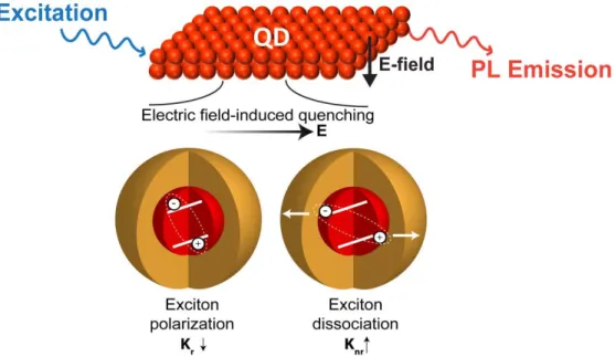
Moreover, the application of an external electric field across QD thin film can spatially polarize the electron and hole wavefunctions of the exciton in opposite directions141, as shown in
Figure 3-1 bottom left. As a result, the reduction in wavefunctions overlap lowers the radiative
recombination rate kr, and therefore reduces 𝜂𝜂𝑃𝑃𝑃𝑃. In addition to the PL quenching, the shift of electron and hole wavefunctions causes a change in the effective bandgap as well as an increase in QD exciton interaction with polar optical phonons. This not only leads to a significant broadening of the PL line but also a concomitant red-shift of the PL spectrum, which is known as the quantum-confined Stark Effect (QCSE)142. In addition, an electric field might also quench QD PL by exciton dissociation (Figure 3-1 bottom right). If the field is large enough, the Coulombic binding of excitons can be overcome, resulting in ionization and the formation of free
49
carriers143. The field-dependent exciton dissociation rate, given by the Onsager-Braun model144, would increase and result in a proportional increase in knr.
Figure 3-1: Schematic (top) of photo-excited QD thin film with an electric field applied across
the QD thin film, and pictures (bottom) illustrate electric field-induced exciton polarization and dissociation processes.
In prior studies performed on single CdSe QDs in solution, substantial PL quenching has been demonstrated with up to 40 meV shift in peak emission at 0.35 MV/cm. In solid-state, Bozyigit et al. used a QD capacitor structure to show that electric field can strongly quench luminance of the QD film in the absence of mobile charge144, with close to 90% max PL suppression achieved at an electric field of 4 MV/cm. Another study by Korlacki et al. investigated the effect of dielectric breakdown at a high electric field by sandwiching a monolayer of QDs between ferroelectric polymers145. Few groups have leveraged QD PL quenching in biological146 or display147 applications. For instance, Rowland et al., adopting the capacitor structure, utilized QD emission to track action potential profile of a firing neuron146. More recently, Salihoglu et al. demonstrated a color-variable PL display that used QD PL quenching to dim selective pixels by directly injecting electric charges into QDs via a graphene
50
layer147. The ultimate degree of PL quenching achieved in previous studies is summarized in
Table 3-1. In many of those studies, the strength of the applied electric field is limited by
dielectric breakdown. Regardless of the cause for the quenching limit, the maximum PL reduction achieved has been 90% (corresponding to the contrast ratio of 10:1) with response time in milliseconds at best. This is still far below the levels required for modern displays, which typically have a contrast ratio of 1000:1 or higher for vivid pixel-to-pixel contrast.
Table 3-1: Summary of previously reported voltage-controlled photoluminescence quenching of
QD ensembles
Reference Year QD Material Maximum PL Quenching
Korlacki et al.145 2011 CdSe in copolymer 90% at 4 MV/cm
Bozyigit et al.148 2012 CdSe/ZnCdS 60% at 3 MV/cm
Bozyigit et al.144 2013 CdSe/CdS 90% at 4 MV/cm
Rowland et al.146 2015 CdSe/ZnSe in PMMA 70% at 0.8 MV/cm
Prasai et al.149 2015 CdSSe on MoS2 75% at 2V
Moebius et al.137 2016 CdSe/CdS 60% at 10V
Scott et al.143 2016 CdSe Nanoplatelets in polymer 28% at 0.13 MV/cm
Rowland et al.150 2017 CdSe/CdS in PMMA 50% at 6-8 MV/cm
51
3.2 QD capacitor device
3.2.1 Device structure and operation
A capacitor structure allows us to apply a large electric field across the QD film without charge injection from the electrodes. The dielectric materials surrounding the QD film have to meet certain requirements. First of all, thin and transparent material with a high dielectric constant is preferred such that a large electric field can be placed across the QD to enable maximum quenching. At the same time, it is important the material is resistive and therefore impedes charge injection from the QD layer. Additionally, it is critical that the QD PL quenching during device fabrication and due to adjacent layers is minimized, especially when putting down layers on top of the QDs.
After some initial material optimization with the dielectric materials (detailed in section 3.2.3), we have developed a preliminary proof-of-concept device, which is shown in Figure 3-2a. The device is comprised of 50 nm of CdSe-CdS QDs sandwiched between two 50 nm HfO2
dielectric layers on ITO patterned substrates. A thin layer (10 nm) of Parylene-C, an insulating polymer often used in passivation coatings, is inserted between QD and top oxide to prevent QD from sputtering damage when depositing top oxide. Indium tin oxide (ITO) and 100 nm of aluminum (Al) are used as bottom and top electrodes, respectively.
52
Figure 3-2: (a) Cross-sectional view of the capacitor device structure with QD sandwiched
between two dielectric layers. (b) PL spectra (top) of the QD film photoluminescence under excitation in ‘ON’ and ‘OFF’ state, and pictures (bottom) of the device in both states with black arrow indicating the operating pixel.
3.2.2 Results and discussion
To study the PL quenching dynamics in the capacitor structure, we perform steady-state PL measurements by applying a forward bias to the device from 0V up to 40V, the QD film is constantly excited by a UV LED. Figure 3-2b shows the QD PL spectrum under a 40V bias and we observe roughly 80% maximum PL suppression as well as an evident spectral red-shift that agrees with field-induced QCSE. Photos at the bottom of Figure 3-2b display the active area of the device, highlighted by the black arrows. It can be clearly observed by the eye that the pixel is on (left) at 0V and is significantly dimmed under 40V bias (right).
PL spectra and the integrated PL intensity as a function of bias applied are illustrated in
Figure 3-3. Significant red-shift and spectral broadening can be observed in Figure 3-3a. As
expected, the normalized PL intensity decreases monotonically with increasing applied field and exhibits PL reduction up to 80% at 40V. Despite the observed PL modulation, the contract ratio