HAL Id: hal-02954038
https://hal-univ-rennes1.archives-ouvertes.fr/hal-02954038
Submitted on 30 Sep 2020
HAL is a multi-disciplinary open access
archive for the deposit and dissemination of
sci-entific research documents, whether they are
pub-lished or not. The documents may come from
teaching and research institutions in France or
abroad, or from public or private research centers.
L’archive ouverte pluridisciplinaire HAL, est
destinée au dépôt et à la diffusion de documents
scientifiques de niveau recherche, publiés ou non,
émanant des établissements d’enseignement et de
recherche français ou étrangers, des laboratoires
publics ou privés.
Narrow and broadband light emission in layered organic
lead halide perovskites: interplay between weak
electron-lattice interactions and defect-related effects
Claudio Quarti
To cite this version:
Claudio Quarti. Narrow and broadband light emission in layered organic lead halide perovskites:
interplay between weak electron-lattice interactions and defect-related effects. Physical Chemistry
of Semiconductor Materials and Interfaces IX, Aug 2020, Online Only, United States. pp.114640Y,
�10.1117/12.2568681�. �hal-02954038�
Narrow and broadband light emission in layered organic lead
halide perovskites: interplay between weak electron-lattice interactions
and defect-related effects
Claudio Quarti*
a,ba
Université de Rennes, ENSCR, INSA Rennes, CNRS, ISCR
(Institut des Sciences Chimiques de Rennes) - UMR 6226, F-35000 Rennes, France
b
Laboratory for Chemistry of Novel Materials, Department of Chemistry,
Université de Mons, Place du Parc 20, Mons 7000, Belgium
*claudio.quarti@umons.ac.be; http://morris.umons.ac.be; https://iscr.univ-rennes1.fr/inorganic-theoretical-chemistry-cti
ABSTRACT
2-Dimensional metal Halide Perovskites (2D-HP) are at the limelight for their potential exploitation in light-emission related applications. In particular, the most-investigated <001>-terminated 2D HP family shows dominant narrow light emission, with reduced Stokes shift, of great interest for display applications. In parallel, these systems often show additional largely Stokes-shifted emission, with reduced spectral resolution, of interest for the lighting application, e.g. development of white light-emitting diodes. Clarifying the emission mechanisms in 2D-HP and explaining the co-existence of these two contrasting emission regimes is greatly coveted, for the further exploitation of this class of semiconductors. Here, Density Functional Theory (DFT) simulations estimate total electron-phonon interaction in 2D-HP in the order of few tens of meV, in agreement with ps-resolved UV-vis measurements, consistent with the reported narrow emission. On the other hand, such small coupling significantly contrasts with the assignment of broadband emission to some form of intrinsic (defect-free) self-trapped exciton. Additional DFT simulations rather assign broadband emission to extrinsic self-trapping, associated to point defects, halide interstitials in particular. This result is in line with similar findings for the parental 3D halide perovskite and highlights, on the one hand, the role of halide defects in lead-halide perovskitoids frames, and explains, on the other hand, the apparent contrasting nature of narrow and broadband emission, as due to two different emission mechanisms. Defect engineering protocol are therefore suggested, to optimize broadband emission in 2D-HP materials.
Keywords: 2-dimensional hybrid lead halide perovskites, light-emission, electron-phonon coupling, point-defects.
1. INTRODUCTION
With first reports tracking back to late nineteenth century,1,2 layered 2-Dimensional metal Halide Perovskites (2D-HP)
are currently facing a second golden era, due to their promising exploitation in opto-electronics. This class of materials has attracted renewed attention following the recent success of their 3-Dimensional (3D) lead halide perovskites analogues in the field of photovoltaic, characterised by an unprecedented and continuous improvement in the corresponding light-to-current conversion efficiency, recently reaching 25.2%.3 In this frame, 2D-HP are currently under
intense investigations for various applications, not solely related to photovoltaics,4 but also displaying,5,6 lasing,7,8 sensors,9 etc. 3D perovskites possess a AMX
3 composition and a specific crystalline structure, corresponding to an
extended network of MX6 octahedral connected in corner-shared fashion, M being a metal, X a halide and A a small
organic cation or alkali atom, filling the spaces between octahedra. 2D perovskites have composition A’2An-1MnX3n+1 and
can be ideally obtained by separating extended corner-shared XM6 planes, as cutting the parental 3D perovskite structure
along specific crystallographic directions, as shown in Figure 1a, by partially or fully substituting the A alkali atom or small cation with bulky A’ cation (common examples are phenylethylammonium or alkylammonium).2,10
Altogether, the spatial confinement of the semiconducting MX6 structure down to a length-scale close to the
De-Broglie wavelength imparts these systems with unique opto-electronic features.10 This, along with their improved stability to moisture,4 as induced by the hydrophobic character of the bulky A’ organic spacer, makes 2D-HP extremely
contrast in the dielectric susceptibility of the inorganic layer (e=5-6) with that of the organic (e =2.5-3.5), result in enhanced electron-hole interaction,10 and consequent formation of stable excitons with sizable (350 – 450 meV11) and
tunable electron-hole binding energy.12 Resulting light emission is characterised by considerable photoluminescence quantum-yield,13 narrow emission (full-width-half-maximum between 20 and 40 meV)2 and reduced Stokes shift (few tens of meV)14 compared to absorption, as shown in Figure 1b, which makes 2D-HP ideal for display applications.
Narrow emission is generally found for inorganic emitters,15,16 where the electron/exciton phonon interaction is weak17
and defect concentration severely controlled, via the use of expensive high-temperature production processes. The neat exciton emission observed in 2D-HP comes therefore with surprise, considering that these materials are produced from solution-based techniques. In this frame, it is worth to mention that several recent investigation pointed out towards additional broadband emission for 2D-HP materials, characterised by very large Stokes shift (600 meV) and reduced spectral resolution (full width half maximum, FWHM~1 eV),18–21 as shown in Figure 1c. Originally observed in <110>
terminated 2D-HP,18 this broadband emission has been observed later-on also in <001>-terminated 2D-HP, although under specific temperature conditions, typically limited to low (<100 K) temperature,21 hence demonstrating this feature
is not exclusive of a precise octahedral connection pattern but is a general property of this class of emitters.
In this perspective, the presence of both narrow exciton light emission and broadband emission is surprising, as it points out towards the coexistence of two different regimes in the optical behaviour of these organic-inorganic semiconductors, specifically a weak exciton-lattice-defect interaction regime, associated to narrow emission, along with a strong exciton-lattice-defect interaction regime, associated to broadband emission. Overall, the deep understanding of the optical behaviour of layered 2D-HP requires a theoretical frame which takes into account not only the electronic structure and exciton features of these systems but which considers also for the perturbations induced by the lattice dynamics (phonons) and defects, as well as the back-perturbation of the excited states on the lattice and defects themselves. Along the direction for the achievement of such ambitious task, I will show here some recent steps forward in the general understanding of the exciton properties of layered halide perovskites. Here, I will discuss the above-mentioned two regimes of 2D-HP. The emerging picture is that 2D HP are generally weakly perturbed to phonons, unlike organic semiconductors,22 or recently synthesised halide double perovkites.23,24 However, 2D HP can be sensitive
to lattice defects, mainly halide interstitials, that induce deep trap states and that can be at the origin of complex photochemical processes,21 leading to broadband emission.
Figure 1. a) derivation of 2D layered metal halide perovskites from the parental 3D perovskite structure; b) Absorbance (blue) and photoluminescence (red) spectra of <001>-terminated methylpropane-1,3-diammonium lead bromine perovskite; c) Temperature resolved PL of (C12H25NH3)2PbI4 perovskite. Figure 1b reproduced with permission from Ref.18 © 2014
2. RESULTS AND DISCUSSIONS
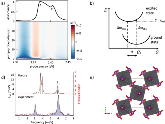
2.1 Narrow emission in 2D HP and weak electron-phonon couplingNarrow emission with reduced Stokes shift is associated to materials with reduced electron-/exciton-phonon coupling, along with low defect density, as typically the case of conventional inorganics semiconductors.17 In this sense, recent efforts have been directed in clarifying the nature and the strength of the electron- and exciton-phonon coupling in 2D-HP.22,25,26 In particular, Ref.22 provides an elegant demonstration of such interaction, along with an estimate of its strength on the order of few tens of meV, using joint experimental/computational approach. Pico-second resolved differential UV-vis transmission measurements have been performed at 5 K for two of the most studied 2D-HP, namely buthylammonium (NBT) and phenylethylammonium (PEA) lead iodide perovskites. In the upper panel of Figure 2a, the steady-state UV-vis absorption of PEA2PbI4 2D-HP is showed close to the exciton resonance. Corresponding differential
transmission spectrum, as measured after pumping at 3.06 eV, is also reported in the Figure 2a, showing the typical negative feature across the A band and a positive feature at the B band. This line-shape is characteristic of a superposition of excitation-induced shift and broadening of the exciton transition by many-body interactions along with the bleach of higher lying electronic states. In the following pico-seconds, we observe the usual exponential decay of the optical signals, as related to the de-excitation of the system, but also a periodic modulation of the signal, which we identify as the signatures of coherent phonons generated via Resonant Impulsive Stimulated Raman Scattering (RISRS) induced by the ultrashort pump pulse. As matter of fact, the present measurement is the time-domain analogue of a Resonant Raman measurement, probing the phonons which most strongly couple with the given electronic transition.
Figure 2. a) steady-state (upper panel) UV-vis spectrum of phenylethylammonium lead iodide 2D-HP, measured at 5K (upper panel) and time-resolved differential transmission spectrum, with pump at 3.06 eV; b) double-well model for potential energy surfaces of ground and excited electronic states, with respect to a general deformation Q. D is the displacement between the minima of the two potentials and lrel is the relaxation energy from the vertical transition to the
minimum of the excited state potential surface; c) comparison of the relaxation energies and Franck-Condon factors from DFT simulations and Fourier-transform spectrum of the oscillatory component of the TA spectrum of buthylammonium lead iodide, at probe energy 2.67 eV; d) Normal mode displacement patter associated to the signal measured at 3 meV. Figure 2a–c reproduced with permission from Ref. 22. © 2019 Springer Nature.
Resonant Raman scattering is often interpreted on the basis of popular displaced harmonic oscillators model in Figure 2b.27 The potential energy surface of the ground and excited state are treated as two harmonic oscillators with
same curvature along the coordinate Q (typically corresponding to the normal modes, in molecules) and displaced by a quantity D. According to the Franck-Condon principle, the ground-to-excited state takes place at the geometry of equilibrium of the ground state, which in the most general case does not correspond to that of the excited state (D¹0), followed by relaxation towards the equilibrium of the excited state, in the fs-ps time-domain. Corresponding relaxation energy lrel depends on the strength of the coupling along the coordinate Q and on the displacement D of the two
oscillators:
!
"#$=
&'
((*
+)
&*
-4
&
-'
/0/(*
+)
&*
-(Eq.1)Eq. 1 requires to evaluate the derivative of the ground to excited transition energy (Eg) with respect to the normal mode
Q, as estimated at the ground state equilibrium structure Q0 (enumerator) and the curvature of the potential energy
surface of the ground/excited state with respect to the normal mode (denominator). In the case of systems having inversion symmetry, selection rules predict zero Raman activity (either resonant or non-resonant) for those normal modes with ungerade (odd) character, which reflects the fact that along these vibrations the two oscillators are not displaced (D=0).
Consistently with the above-mentioned theoretical frame, we performed periodic Density Functional Theory calculations, within the Linear Combination of Atomic Orbitals formalism, as implemented in the CRYSTAL17 package,28 and we computed the quantities needed in Eq. 1, namely, normal modes of vibration at the electronic ground
state, corresponding curvatures, and the derivative of the ground-to-excited state electronic transition, with respect to the displacement patter for each normal mode. In the present case, the ground-to-excited state electronic transition was roughly approximated with the lowest energy band-to-band transition. Our theoretical predictions for NBT2PbI4 2D-HP
in Figure 2c nicely parallel the measured RISRS signals from differential transmission spectrum, as probed at an energy close to the band-to-band transition, at 2.67 eV, supporting the general theoretical frame. We found two sets of phonons which couple to the band-to-band electronic transition, around 3-4 meV (~25-32 cm-1), and around 5 meV (~40 cm-1), respectively. Displacement patter associated to the most interacting normal mode at 3 meV is showed in Figure 2d. Computed frequencies for the low energy phonons in Figure 2c are slightly underestimates, compared to experiment, but it is worth to stress that the accurate prediction of normal modes at such low frequency range is inherently complicated by the shallow form of the potential energy surface and by anharmonic effects. As the main interest in the optical properties of 2D HP is related to their excitonic properties, the RISRS signal was also measured at probe energy corresponding to the A and B signals in Figure 2a. In particular, tuning the RISRS signal for probe at 2.36 eV, corresponding to the lowest energy excitonic A state, the highest phononic component at 5 meV was shown to be dominant, while the component at 3-4 meV was much less important.22 From a theoretical and computational viewpoint,
estimating the deformation-of-potential electron-phonon interaction via Eq. 1 can be conceptually performed, inherently considering electron-hole interaction, via for instance Time Dependent-Density Functional Theory (TD-DFT) or the solution of the Bethe-Salpeter Equation (BSE). However, TDDFT calculations were shown to not accurately account for the electron-hole screening, with final exciton binding energy being highly sensitive with respect to the amount of exact exchange used in the definition of the exchange-correlation kernel.29 In contrast, ab-initio solution of the Bethe-Salpeter
Equations (BSE) performed on electronic structure from GW approximation was shown to provide exciton binding energy nicely matching the experimental datum, at least for the lowest energy 1s-component of the Rydberg series.30 On the other hand, the computational cost of this methodology makes it unsuitable for similar study as the one reported in Ref. 22, as the latter requires several BSE calculations, via distorting the crystalline structure along the different normal
modes. In this sense, the availability of simplified methods for the simulation of excited states would be greatly needed, to further clarify these problems.11 Altogether, total relaxation energy can be estimated from the sum of the relaxation energies computed for each phonon, which sums up to ca. 46 meV, that is ca. 2 times kT, in fair agreement with the measured Stokes shift. The general picture coming out is that, although not being completely transparent to lattice dynamics, excitons in 2D HP are just weakly perturbed by phonons. This seems not the case, for instance, for recently reported halide double perovskites.23,24 Cortecchia and co-workers provide slightly contrasting results from DFT
the displacement is along convenient set of coordinates (e.g. phonons) and the amount of distortion is in line with curvature of the potential energy surface. In other words, the perturbation of the electronic structure in Ref. 20 can be
overestimated, as result of an unrealistic distortion of the lattice.
Figure 3. a) energy level scheme associated to the narrow emission (ħwemi) and broad band emission (ħwbroad); b-d)
crystalline model and corresponding projected Density Of States (DOS) for 2D (C6H13NH3)2PbI4 HP without defects (b),
containing one iodide vacancy with +1 charge (c) and containing an interstitial iodide with -1 charge (interstitial, circled in red). Figure 3b–d reproduced with permission from Ref. 21© 2017 Americal Chemical Society.
2.2 Broadband emission in 2D HP as due to defect induced electron-lattice interaction
In light of the previous results, presence of broad-band emission in 2D-HP comes with even more surprise, as this openly contrasts with the RISRS signals measured by Thouin et al. in Ref. 22 and the corresponding weak electron phonon coupling computed from deformation-of-potential. Of course, other electron-phonon coupling mechanisms, as Frölich interactions, can be invoked, which, in light of different selection rules, may not be probed via RISRS.17 On the other
hand, it is worth to stress that the assumption of large electron-phonon interaction is in open contrasts with the observed narrow emission, which at least for <001>-terminated 2D HP is ubiquitous with the temperature. In other words, if the lattice were going to sizably rearrange in response to the formation of photogenerated species (either free-charges or electron-hole exciton pairs), one would expect such relaxation to be general and independent from external factors, for instance the temperature, and should therefore result in the suppression of the narrow emission. In this sense, in their review Karunadasa and co-workers, nicely distinguished between intrinsic and extrinsic self-trapping, as responsible for the broadband emission in 2D-HP.2 Intrinsic self-trapping does not requires imperfections in the material structure and is therefore characteristic of the lattice itself, that means, it implicitly assumes sizable electron-phonon coupling, as discussed above. Extrinsic self-trapping instead requires the presence of defects or imperfections in the lattice to kick-off the mechanism of self-trapping for the excitons, hence potentially opening new channels for the exciton decay in 2D-HP (either radiative or non-radiative), alternative to the narrow emission, as schematically depicted in Figure 3a. In this sense, the presence of different types of defects and/or different defect configurations in the material potentially explains the emission broadening, as due to not a single and well defined decay mechanism but to a manifold of decay mechanisms, with slightly different energetics. Aiming to investigate the possible role of point defects on the optical properties of 2D HP, I performed periodic DFT calculations for supercell models of hexylammonium lead iodide perovskite, containing different types of point defects, namely metal/halide vacancies/interstitials.21 Resulting atomic
projected Density Of State for the non-defective model, as computed using standard PBE exchange correlation functional, is shown in Figure 3b-d. The DFT band gap computed for the non-defective model (Figure 3b) is obviously underestimated, because of the unbalanced error induced by the lack of spin-orbit coupling and inaccurate treatment of electronic many-body effects (as typical of the employed PBE exchange correlation functional).29 Still, the
Valence/Conduction Band Edge of the material are related to outer-shell p-states of the iodine and to 6s-states of lead, as widely reported in the literature.29,31,32 The introduction of charged (+1) halide vacancy in the model (VI+1) only weakly
perturbs the electronic structure, mainly in correspondence of the conduction band, as shown in Figure 3c, while the introduction of charged (-1) iodine interstitial defect (II-1) interestingly results in the formation of intragap deep trap
states, associated to the interstitial halide itself, as shown in Figure 3d. Further tests were performed on the iodine-related Frenkel defect as composed by the vacancy-interstitial iodide pair, to verify that the DFT results are not biased by the used of background charges. Additionally, effect of Spin-Orbit Coupling (SOC) and of Hubbard correction on the band gap were checked, always finding deep trap states associated to the interstitial iodine species.21
Interstitial lead defects have been also found to significantly perturb the electronic structure of the system, via the formation of PbI2 molecular species and consequent introduction of deep trap states into the electronic structure of
2D-HP.21 Interestingly, the results in Figure 3 go on pair with similar results for their 3D HP analogues, highlighting the
potential role of interstitial halides as electron acceptors.33 Meggiolaro and coworkers in fact computed the defect formation energy for various types of point defects (metal/halide interstitials/vacancies), finding that interstitial iodine defects form similar deep trap states for widely investigated methylammonium lead iodide 3D perovskite, as in Figure 3d. Therefore, these authors proposed possible photochemical-mechanisms related to charge trapping and sub-band gap light emission in 3D HP, with reference to experimental UV-vis measurements.33,34 In this frame, more investigations are required to unveil the detailed mechanism behind the broadband emission, which can potentially involve the trapping of the photogenerated holes into the interstitial halide deep trap states or impose more complicated pathways, but this common role of iodine-related point defects in 2D in Ref. 21 and 3D HP in Ref. 33 is clearly of interest
to understand the photophysics of halide perovskite systems. Namely, the connection between defects and broadband emission can have important technological consequences, as it paves the way for the development of a “defect-engineering” protocol, for the optimization of this type of emission for light illumination applications.
3. CONCLUSIONS
The optoelectronic response of semiconductors is often the result of a complex interplay between direct/indirect electronic structure, symmetry related properties, and effects related to the perturbation of the lattice associated to the lattice dynamics (i.e. phonons). In the case of solution-based processable materials, further effects are often related to the almost unavoidable presence of structural defects. 2-Dimensional, metal Halide Perovskites (2D-HP) perfectly epitomize this situation, showing, at least for the family of <001>-terminated 2D-HP (see Figure 1a), two regimes of light emissions, one characterized by small Stokes-shifted, narrow emission and the other by large Stokes-shifted, broadband emission. In the present contribution, I try to provide a global perspective about the mechanisms at the atomistic scale dictating these two features in the photophysics of 2D-HP. Narrow emission is consistent with weak exciton/electron-phonon coupling in the range of few tens of meV, as obtained from Density Functional Theory (DFT) calculations and Resonant Impulsive Stimulated Raman Scattering (RISRS) measurements. Such weak exciton/electron-phonon coupling regime resembles the typical behavior of conventional inorganic semiconductors and strongly criticizes the assignment of the broadband, Stokes-shifted emission to intrinsic self-trapped excitons. Furthermore, these results inherently call for the effect of some defect or perturbation in the lattice, as starter for the self-trapping mechanism. In this frame, our Density Functional Theory simulations, as performed on defective crystalline supercell models, highlight the presence of deep-trap states associated to point defects, interstitial halides in particular, with energetics consistent with the measured Stokes shift. Further works will be needed to clarify the mechanism behind the broadband emission in 2D HP. Still, the present contribution smoothly connects the (apparently contrasting) narrow emission of 2D-HP with observed broadband emission. Furthermore, it also links the role of halide defects in 2D-HP and in their 3D analogues, as highlighted by Meggiolaro and coworkers.33 The proposed connection of broadband emission of point-defects can be at the basis of the
optimization of broadband emission via “defect-engineering” protocol, aimed to stabilize the defects with the temperature and minimize non-radiative recombination.
ACKNOWLEDGEMENTS
REFERENCES
[1] Topsøe, H., “Krystallographisch-Chemische Untersuchungen Homologer Verbindungen” Z. Kristallogr. - Cryst. Mater., 8, 246 (1884).
[2] Smith, M.D., Connor, B.A., and Karunadasa, H.I., “Tuning the Luminescence of Layered Halide Perovskites” Chem. Rev., 119, 3104–3139 (2019).
[3] “https://www.nrel.gov/pv/cell-efficiency.html.”
[4] Tsai, H., Nie, W., Blancon, J.-C., Stoumpos, C.C., Asadpour, R., Harutyunyan, B., Neukirch, A.J., Verduzco, R., Crochet, J.J., et al., “High-efficiency two-dimensional Ruddlesden– Popper perovskite solar cells” Nature, 536, 312–316 (2016).
[5] Dou, L., Wong, A. b., Yu, Y., Lai, M., Kornienko, N., Eaton, S.W., Fu, A., Bischak, C.G., Ma, J., et al., “Atomically thin two-dimensional organic-inorganic hybrid perovskites” Science, 349, 1518–1521 (2015). [6] Tsai, H., Nie, W., Blancon, J.-C., Stoumpos, C.C., Soe, C.M.M., Yoo, J., Crochet, J.J., Tretiak, S., Even, J., et al.,
“Stable Light-Emitting Diodes Using Phase-Pure Ruddlesden–Popper Layered Perovskites” Adv. Mater., 30, 1704217 (2018).
[7] Leyden, M.R., Matsushima, T., Quin, C., Ruan, S., Ye, H., and Adachi, C., “Amplified spontaneous emission in phenylethylammonium methylammonium lead iodide quasi-2D perovskites” Phys. Chem. Chem. Phys., 20, 15030–15036 (2018).
[8] Liang, Y., Shang, Q., Wei, Q., Zhao, L., Liu, Z., Zhong, Y., Chen, J., Gao, Y., Li, M., et al., “Lasing from Mechanically Exfoliated 2D Homologous Ruddlesden–Popper Perovskite Engineered by Inorganic Layer Thickness” Adv. Mater., 31, 1903030 (2019).
[9] Deng, W., Zhang, X., Huang, L., Xu, X., Wang, L., Wang, J., Shang, Q., Lee, S.-T., and Jie, J., “Aligned
Single-Crystalline Perovskite Microwire Arrays for High-Performance Flexible Image Sensors with Long-Term Stability” Adv. Mater., 28, 2201–2208 (2016).
[10] Katan, C., Mercier, N., and Even, J., “Quantum and Dielectric Confinement Effects in Lower-Dimensional Hybrid Perovskite Semiconductors” Chem. Rev., 119, 3140–3192 (2019).
[11] Blancon, J.-C., Stier, A.V., Tsai, H., Nie, W., Stoumpos, C.C., Traoré, B., Pedesseau, L., Kepenekian, M., Katsutani, F., et al., “Scaling law for excitons in 2D perovskite quantum wells” Nat. Commun., 9, 2254 (2018). [12] Smith, M.D., Pedesseau, L., Kepenekian, M., Smith, I.C., Katan, C., Even, J., and Karunadasa, H.I., “Decreasing
the electronic confinement in layered perovskites through intercalation” Chem. Sci., 8, 1960–1968 (2017). [13] Kawano, N., Koshimizu, M., Sun, Y., Yahaba, N., Fujimoto, Y., Yanagida, T., and Asai, K., “Effects of Organic
Moieties on Luminescence Properties of Organic− Inorganic Layered Perovskite-Type Compounds” J. Chem. Phys. C., 118, 9101–9106 (2014).
[14] Hong, X., Ishihara, T., and Nurmikko, A.V., “Photoconductivity and Electroluminescence in Lead Iodide Based Natural Quantum Well Structures” Solid State Commun., 84, 657–661 (1992).
[15] Saito, H., and Sugou, S., “A narrow photoluminescence linewidth of 21 meV at 1.35 µm from strain-reduced InAs quantum dots covered by In0.2Ga0.8As grown on GaAs substrates” Appl. Phys. Lett., 74, 1111 (1999).
[16] Kim, Y.-H., Cho, H., and Lee, T.-W., “Metal halide perovskite light emitters” PNAS, 113, 11694–11702 (2016). [17] Yu, P.Y., and Cardona, M., [Fundamentals of Semiconductors] , 3rd ed., Springer: Berlin, Heidelberg, Germany,
New York (2005).
[18] Dohner, E.R., Hoke, E.T., and Karunadasa, H.I., “Self-Assembly of Broadband White-Light Emitters” J. Am. Chem. Soc., 136, 1718–1721 (2014).
[19] Yangui, A., Garrot, D., Lauret, J.S., Lusson, A., Bouchez, G., Deleporte, E., Pillet, S., Bendeif, E.E., Castro, M., et al., “Optical Investigation of Broadband White-Light Emission in Self- Assembled Organic−Inorganic Perovskite (C6H11NH3)2PbBr4” J. Phys. Chem. C., 119, 23638–23647 (2015).
[20] Cortecchia, D., Yin, J., Bruno, A., Alencious Lo, S.-Z., Gurzadyan, G.G., Mhaisalkar, S., Brédas, J.-L., and Soci, C., “Polaron self-localization in white-light emitting hybrid perovskites” J. Mater. Chem. C., 5, 2771–2780 (2017).
[21] Booker, E.P., Thomas, T.H., Quarti, C., Stanton, M.R., Dashwood, C.D., Gillett, A.J., Richter, J.M., Pearson, A.J., Davis, N.J.L.K., et al., “Formation of Long-Lived Color Centers for Broadband Visible Light Emission in Low-Dimensional Layered Perovskites” j. Am. Chem. Soc., 139, 18632–18639 (2017).
[22] Thouin, F., Valverde-Chavéz, D.A., Quarti, C., Cortecchia, D., Bargigia, I., Beljonne, D., Petrozza, A., Silva, C., and Kandada, A.R.S., “Phonon coherences reveal the polaronic character of excitons in two-dimensional lead halide perovskites” Nat. Mater., 18, 349–356 (2019).
[23] Steele, J.A., Puech, P., Keshavarz, M., Yang, R., Banerjee, S., Debroye, E., Kim, C.W., Yuan, H., Heo, N.H., et al., “Giant Electron−Phonon Coupling and Deep Conduction Band Resonance in Metal Halide Double Perovskite” ACS Nano, 12, 8081–8090 (2018).
[24] Zelewski, S.J., Urban, J.M., Surrente, A., Maude, D.K., Kuc, A., Schade, L., Johnson, R.D., Dollmann, M., Nayak, P.K., et al., “Revealing the nature of photoluminescence emission in the metal-halide double perovskite
Cs2AgBiBr6” J. Mater. Chem. C., 7, 8350–8356 (2019).
[25] Straus, D.B., Parra, S.H., Iotov, N., Gebhardt, J., Rappe, A.M., Subotnik, J.E., Kikkawa, J.M., and Kagan, C.R., “Direct Observation of Electron−Phonon Coupling and Slow Vibrational Relaxation in Organic−Inorganic Hybrid Perovskites” J. Am. Chem. Soc., 138, 13798–13801 (2016).
[26] Ni, L., Huynh, U., Cheminal, A., Thomas, T.H., Shivanna, R., Hinrichsen, T.F., Ahmad, S., Sadhanala, A., and Rao, A., “Real-Time Observation of Exciton−Phonon Coupling Dynamics in Self-Assembled Hybrid Perovskite Quantum Wells” ACS Nano, 11, 10834–10843 (2017).
[27] Coropceanu, V., Cornil, J., da Silva Filho, D.A., Olivier, Y., Silbey, R., and Brédas, J.-L., “Charge Transport in Organic Semiconductors” Chem. Rev., 107, 926–952 (2007).
[28] Dovesi, R., Erba, A., Orlando, R., Zicovich-Wilson, C.M., Civalleri, B., Maschio, L., Rérat, M., Casassa, S., Baima, J., et al., “Quantum-mechanical condensed matter simulations with CRYSTAL” WIREs Comput. Mol. Sci., 8, e1360 (2018).
[29] Quarti, C., Marchal, N., and Beljonne, D., “Tuning the Optoelectronic Properties of Two-Dimensional Hybrid Perovskite Semiconductors with Alkyl Chain Spacers” J. Phys. Chem. Lett., 9, 3416–3424 (2018).
[30] Giorgi, G., Yamashita, K., and Palummo, M., “Nature of the Electronic and Optical Excitations of Ruddlesden– Popper Hybrid Organic–Inorganic Perovskites: The Role of the Many-Body Interactions” J. Phys. Chem. Lett., 9, 5891–5896 (2018).
[31] Even, J., Pedesseau, L., Dupertuis, M.-A., Jancu, J.-M., and Katan, C., “Electronic model for self-assembled hybrid organic/perovskite semiconductors: Reverse band edge electronic states ordering and spin-orbit coupling” Phys. Rev. B., 86, 205301 (2012).
[32] Umebayashi, T., Asai, K., Kondo, T., and Nakao, A., “Electronic structures of lead iodide based low-dimensional crystals” Phys. Rev. B., 67, 155405 (2003).
[33] Meggiolaro, D., Motti, S.G., Mosconi, E., Barker, Alex.J., Ball, J., Perini, C.A.R., Deschler, F., Petrozza, A., and De Angelis, F., “Iodine chemistry determines the defect tolerance of lead-halide perovskites” Energy Environ. Sci., 11, 702–713 (2018).
[34] Hoke, E. T., Slotcavage, D.J., Dohner, E.R., Bowring, A.R., Karunadasa, H.I., and McGehee, M.D., “Reversible photo-induced trap formation in mixed-halide hybrid perovskites for photovoltaics” Chem. Sci., 6, 613–617 (2015).