HAL Id: hal-02390974
https://hal.archives-ouvertes.fr/hal-02390974
Submitted on 1 Dec 2020
HAL is a multi-disciplinary open access
archive for the deposit and dissemination of
sci-entific research documents, whether they are
pub-lished or not. The documents may come from
teaching and research institutions in France or
abroad, or from public or private research centers.
L’archive ouverte pluridisciplinaire HAL, est
destinée au dépôt et à la diffusion de documents
scientifiques de niveau recherche, publiés ou non,
émanant des établissements d’enseignement et de
recherche français ou étrangers, des laboratoires
publics ou privés.
A Vector Modulation Strategy for Open-End Winding
Conversion Systems
Frederico Matos, Herbert Ramos, Caio Oliveira, Victor Mendes, Marcos
Mendes, Thierry Meynard
To cite this version:
Frederico Matos, Herbert Ramos, Caio Oliveira, Victor Mendes, Marcos Mendes, et al.. A Vector
Mod-ulation Strategy for Open-End Winding Conversion Systems. 2018 IEEE International Conference on
Industrial Technology (ICIT), Feb 2018, Lyon, France. �10.1109/ICIT.2018.8352249�. �hal-02390974�
A Vector Modulation Strategy for
Open-End Winding Conversion Systems
Frederico F. V. Matos
∗, Herbert O. Ramos
∗, Caio E. Oliveira
∗, Victor F. Mendes
∗Marcos A. S. Mendes
∗and Thierry Meynard
† ∗Graduate Program in Electrical EngineeringFederal University of Minas Gerais, Brazil Email: [email protected] †Institut National
Polytechnique de Toulouse University of Toulouse, France
Abstract—With the increasing demand for industrial processes for power rating, quality and faster dynamics, multilevel converters and
structures have been developed and became popular. Among them, the open-end winding topology is an advantageous structure for its lower device count and switching redundancy.
This paper presents a vector modulation technique for one of these systems, which employs a pair of two-level converters, being equivalent to a traditional three-level system. The strategy uses the nearest space vectors to the reference in order ensure a good power quality on the output. Its main features are the balance of commutations among devices, its constant switching rate and the higher frequency current ripple.
The characteristics of the fixed switching patterns to obtain the best quality on the output are presented along with simulation results that demonstrate the accomplishment of the strategy goals.
Index Terms—Open-End Winding, Modulation Techniques, Space Vector Modulation, Power Conversion.
I. INTRODUCTION
Over the last decades, several multilevel converter topologies were developed in order to achieve superior power, energy quality or dynamics than the traditional two level structure. Among them, the neutral point clamped (NPC), flying capacitor (FC) and cascaded H-bridge (CHB) achieved higher acceptance and became widely known [1].
The open-end winding (OEW) drive system is a connection scheme that uses two power converters to achieve a higher number of voltage levels in the electrical machine than the converters are individually capable of. It was first presented by Guggenbach and Stemmler in 1993 [2]. Fig. 1 shows a system that employs two-level converters in an open winding configuration, corresponding to a three-level drive.
The main advantages of this structure are the lower device count compared to traditional Δ/Y systems, the amount redundant switching states, and the absence of the capacitor voltage balance problems present in NPC or FC converters. However, in order to avoid the circulation of common-mode currents, the dc-links must be isolated in the grid side [2].
OEW structures have been reported for several applications, such as electrical and hybrid vehicles [3], aerospace [4], water pumping solar systems [5], [6] and wind power [7], [8], to name a few. Also, the combination of power converters
Fig. 1. Open end winding drive.
As for the modulation, several techniques were developed specifically for OEW systems, as the sub-hexagon strategies in [13]– [15] and the carrier based in [16]–[18]. These techniques, however, propose an alternating role between converters: one is clamped while the other is effectively switched.
In this work, a vector modulation technique is presented where all switches are switched constantly and the voltage reference nearest space vectors are used in order to achieve the best performance with respect to harmonic distortion. These characteristics are particularly interesting for high power, high voltage devices.
II. MODULATION TECHNIQUE
Fig. 2 presents the voltage space vectors produced in the machine windings by the system from Fig. 1. There are 19 distinct space vectors (including the null vector), with 26 = 64 different switching states.
The space vector modulation technique consists of applying the vectors located closest to the reference voltage space
Fig. 2. Voltage space vectors for the three-level power converter.
vector in such a manner that their linear combination over one switching period corresponds to the reference vector. The nearest vectors depend on the magnitude and angle of the reference and can be found by dividing the hexagon of space vectors produced by the system into triangular regions, as shown in Fig. 2.
Six sections are named from A to F, depending on the angle of the reference vector, and each section is divided in triangular subsections from 1 to 4. When the reference voltage is inside one specific region, the vertexes of that region correspond to the nearest voltage space vectors i.e., when in region A4, vectors V3, V4 and V5 are the closest vectors.
Fig. 2 also shows that for every region there are three time variables, ta, tb and tc, each associated to one of the triangle vertexes. When each vertex is applied for its corresponding time, their linear combination in one switching period corresponds to the reference voltage. They are obtained by solving the system of equations
Vata +Vbtb +Vctc = VrefTs
(1)
ta +tb +tc = Ts
where Ts is the switching period, Vref = V∗ejθ is the reference vector and Va, Vb and Vc are the vectors associated to ta, tb and tc, depending on the region. For region A4, as an example, V5 = 2Vdcej60◦corresponds to ta, V3 to tb, and V4 to tc. The solutions of (1) for each subsection were presented by [19] and are comprised in Table I. In the resulting
expressions, the modulation index is k = V∗/(Vdc√3) and the angle is θˆ= θ (mod 60◦).
A. Switching Patterns
While the time variables calculation is not related to the converter topology itself but to the number of levels; the next step in the modulation technique is intimately related to the structure. It is the selection of which switching states are to
Fig. 3. Possible vector transitions for region A2.
be used in order to apply the corresponding vectors, and on what sequence.
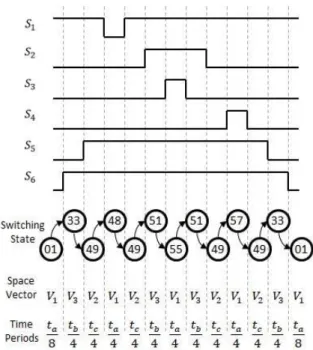
To facilitate the representation of the switching states, we will use decimal numbers that, converted to a 6-bit binary number, represent the switches S1 to S6, from the least to the most significant bit. To exemplify: vector 19 corresponds to the switching state 010011, which means that switches S1, S2 and S5 are closed.
Fig. 3 presents the switching states for vectors V1, V2 and V3, that define region A2. The arrows linking each state correspond to possible direct transitions, where only one switch is commutated.
In order to identify the best possible switching patterns (or sequences) regarding power quality and loss distribution among devices, some conditions were determined: • The patterns should have the highest number of states as possible, in order to reduce the current ripple;
• The switching frequency should be the same for all six converter legs, in other words during a switching period each device
can commutate two times only;
• The resulting voltage waveform must be symmetrical: there are switching patterns that produce waveforms with full symmetry around half the switching period, and the resulting voltages are centered around one quarter. That results in higher frequency current ripple;
• The starting (and ending) switching states of the patterns for each region are chosen in order to reduce the commutation number when the reference moves to a neighbor region. As an example, regions A1, A2, A3 and F4 share the vector V1, so we’ll choose the same V1 state (01 for example) to begin these regions patterns. The same is valid for B1, B2, B3 and A4 with vector V4, and so on.
Taking those constraints into account, we could identify a considerable number of distinct switching patterns for each one of the regions. Fig. 4 presents one of these patterns, for
TABLE I EQUATIONS FOR VECTOR APPLICATION TIME PERIODS.
1 2 3 4
Fig. 4. Switching pattern for region A2.
region A2, and its corresponding command pulses over one switching period.
One can notice that the pattern is composed of 13 switching states, which corresponds to the maximum number of commutations per switching period. The resulting voltage space vector sequence shows a repetition by half the switching period, and a symmetry by one quarter this time. Application times ta, tb and tc are divided along the repeating vectors in order to equalize the output, reducing ripple.
Finally, one pattern was selected for each region, forming a table which is presented in Appendix A. III. DIGITAL IMPLEMENTATION
Although this vector modulation principle has not a straightforward implementation such as the methods based on reference-carrier comparison, a digital implementation is achievable through the use of a lookup table.
The inputs of the modulation algorithm are the previously defined modulation depth k = V∗/(Vdc√3) and the space vector angle θ of the voltage reference. The first step is to localize which
is the region where it is situated: while the section is directly given by the reference angle, subsection can be found by using equations
Subsection 4: k sin(θˆ) > 1/2
Subsection 1: k cos(θˆ−30◦) < 1/2
(2) Subsection 2: k cos(θˆ+30◦) > 1/2
Subsection 3: None of the previous where θˆ= θ (mod 60◦), just as in Table I.
Once the subsection is known, the equations from Table I are used to define ta, tb and tc. Now, in order to apply the switching pattern correctly, a triangular counter and six compare variables are used. Their comparison defines which one of the switching states from the lookup table must be used. Fig. 5 illustrate this principle, making use of the previous example of switching pattern for the region A2.
If we consider that the counter goes from zero to Ts/2 and back to zero, then, in this example
cmp1 = ta/8 cmp2 = cmp1 +tb/4
cmp3 = cmp2 +tc/4
(3) cmp4 = cmp3 +ta/4 cmp5 = cmp4 +tc/4 cmp6 = cmp5 +tb/4
Finally, with all switching states, for all regions, saved in a lookup table, an initial address is determined by the section and subsection information. The crossings between the counter and the different compare variables define which switching state must be assessed from that initial address in order to apply the command pulses at the output of the system.
Now, an important feature of the patterns selection can help improve the harmonic content at the output: the type of voltage symmetry that exists in the switching patterns allow to use a discretization time of Ts/4 to update the compare variables. As the
pattern voltages repeat twice in one switching
period and are pair functions, this does not result in additional commutations.
Fig. 5. Counter-compare scheme to determine instantaneous switching state application.
Fig. 6. Winding steady state voltage and current.
IV. SIMULATION RESULTS
The vector modulation technique was implemented in simulation using Plexim’s PLECS software in order to verify its functionality. A power structure such as that from Fig. 1, but with an RL load, was simulated. Simulation parameters are presented in Appendix B.
Fig. 6 presents the voltage and current directly on one of the windings while the modulation index is set to its rated value. It can be seen that the voltage presents a total of 9 distinct levels, because of the resulting zero sequence, and its maximum value is 4/3Vdc.
The current has a low ripple with higher frequency than that of the switching, as a result of the symmetry of the commutation patterns. The harmonic spectrum is presented in Fig. 7. Aside from the traditional low frequency harmonics,
Fig. 7. Winding current harmonic spectrum.
Fig. 8. Gate pulses for three switching periods and the respective reference region.
the ripple appears in fact around four times the commutation frequency, which is a very attractive feature for a modulation technique especially for systems with high power, high voltage devices.
Another important feature of the switching patterns selection is the number of commutations during the transition between regions. Fig. 8 shows all the gate pulses during three switching periods and the location of the reference, in other words, the region where it is located. The two vertical lines, I and II, delimit the commutation periods.
We can observe that, with the processing period of Ts/4, region transition can occur inside a switching period and more than
one time.
At the first and third periods, there is a transition from A4 to B2 and C2 to C3, respectively. Those transitions happen in different instants, half and three quarter the period, and does not introduce additional commutations, with the proposed switching patterns. However, from subsections 3 to 4, as it is the case of the second period shown (B3 to B4), the change of pattern introduces one additional commutation of the switch S1, which is highlighted. This is the minimum number of such additional switchings per section, so what the proposed scheme does to minimize its relevance is to equilibrate them among the switches.
V. CONCLUSION
In this paper, a vector modulation strategy for a three-level open-end winding drive system using two-level converters was presented.
The modulation technique consists of using the nearest voltage space vectors produced by the system to form a linear combination that corresponds to the reference. A methodology to obtain the switching patterns for this system is presented which leads to commutation sequences with a permanent switching frequency for all switches, a current ripple with double this frequency and an equilibrated number of commutations per fundamental period.
Simulation results have shown the achievement of these objectives which are specially beneficial to systems with high power, high voltage semiconductor devices where commutation losses are a key issue.
APPENDIX A SWITCHING PATTERNS A1 A2 A3 A4 B1 00→32→40→56→58→59→63→59→58→56→40→32→00 B2 B3 B4 C1 C2 02→10→42→40→42→46→47→46→42→58→42→10→02 C3 02→10→08→40→44→46→47→46→62→58→26→10→02 C4 D1 D2 D3 D4 04→12→28→24→28→30→31→30→28→60→28→12→04 E1 00→04→05→07→23→31→63→31→23→07→05→04→00 E2 04→20→28→24→28→29→31→29→28→60→28→20→04 E3 04→20→16→24→25→29→31→29→61→60→52→20→04 E4 05→21→20→16→20→21→23→21→29→61→29→21→05 F1 00→16→48→56→57→61→63→61→57→56→48→16→00 F2 05→21→17→16→17→21→23→21→53→61→53→21→05 F3 05→01→17→16→17→19→23→55→53→61→53→37→05 F4 01→17→49→48→49→53→55→53→49→57→49→17→01 APPENDIX B SIMULATION PARAMETERS Parameter Value
Load power factor 0.95 Switching frequency 540Hz
ACKNOWLEDGMENT
The authors would like to thank the Brazilian agencies CNPq and CAPES, the French agency COFECUB and LAPLACE laboratory, for their support to this research.
REFERENCES
[1] J. Rodriguez, L. G. Franquelo, S. Kouro, J. I. Leon, R. C. Portillo, M. A. M. Prats, and M. A. Perez, “Multilevel converters: An enabling technology for high-power applications,” Proceedings of the IEEE, vol. 97, pp. 1786–1817, 2009.
[2] P. Guggenbach and H. Stemmler, “Configurations of high power voltage source inverter drives,” Fifth European Conference on Power Electronics and Applications, vol. 5, pp. 7–14, 1993.
[3] E. Levi, M. Jones, and W. Satiawan, “A multiphase dual-inverter supplied drive structure for electric and hybrid electric vehicles,” in Vehicle Power and Propulsion Conference (VPPC), 2010 IEEE. IEEE, 2010, pp. 1–7.
[4] S. Mohan, J. S. TK, A. Gopinath, B. Jaya, and M. Namboothiripad, “Modeling and simulation of high power open end winding based electromechanical actuator for aerospace applications,” in Power and Advanced Control Engineering (ICPACE), 2015 International Conference on. IEEE, 2015, pp. 36–41. [5] S. Jain, R. Karampuri, and V. Somasekhar, “An integrated control algorithm for a single-stage pv pumping system using an open-end winding induction
motor,” IEEE Transactions on Industrial Electronics, vol. 63, no. 2, pp. 956–965, 2016.
[6] A. S. Abdel-Khalik, A. Elserougi, A. M. Massoud, and S. Ahmed, “A cascaded boost inverter-based open-end winding three-phase induction motor drive for photovoltaic-powered pumping applications,” in Electric Power and Energy Conversion Systems (EPECS), 2015 4th International Conference on. IEEE,
2015, pp. 1–6.
[7] T. A. Lipo and D. Pan, “Series compensated open-winding pm generator wind generation system,” 15th International Power Electronics and Motion Control Conference, vol. 7c, pp. 1–8, 2012.
[8] J. Chivite-Zabalza, I. Larrazabal, I. Zubimendi, S. Aurtenetxea, and M. Zabaleta, “Multi-megawatt wind turbine converter configurations suitable for off-shore applications, combining 3-l npc pebbs,” IEEE Energy Conversion Congress and Exposition, pp. 2635 – 2640, 2013.
[9] G. A. Carlos, R. P. Sousa, C. B. Jacobina, J. P. Mello, L. M. Barros, and A. C. Oliveira, “Three-phase drive systems based on oew configurations with reduced controlled switch count,” in Power Electronics Conference and 1st Southern Power Electronics Conference (COBEP/SPEC), 2015 IEEE 13th Brazilian. IEEE, 2015, pp. 1–6.
[10] M. Darijevic, M. Jones, and E. Levi, “An open-end winding four-level five-phase drive,” IEEE Transactions on Industrial Electronics, vol. 63, no. 1, pp. 538–
549, 2016.
[11] T. A. Lipo, Y. Wang, D. Panda, and D. Pan, “Open-winding power conversion systems fed by half-controlled converters,” IEEE Transactions on Power Electronics, vol. 28, pp. 2427–2436, 2013.
[12] C. B. Jacobina, N. Rocha, and N. S. M. L. Marinus, “Open-end winding permanent magnet synchronous generator system with reduced controlled switch count,” Brazilian Power Electronics Conference, pp. 692–698, 2013.
[13] K. Gopakumar, E. Shivakumar, S. K. Sinha, A. Pittet, and
V. .T.Ranganathan, “Space vector pwm control of dual inverter fed openend winding induction motor drive,” Sixteenth Annual IEEE Applied Power
Electronics Conference and Exposition, vol. 1, pp. 399–405, 2001.
[14] V. Somasekhar, S. Srinivas, and K. Gopakkumar, “A space vector based pwm switching scheme for the reduction of common-mode voltages for a dual inverter fed open-end winding induction motor drive,” in Power Electronics Specialists Conference, 2005. PESC’05. IEEE 36th. IEEE, 2005, pp. 816–821.
[15] S. Srinivas and V. Somasekhar, “Space-vector-based pwm switching strategies for a three-level dual-inverter-fed open-end winding induction motor drive and their comparative evaluation,” IET Electric Power Applications, vol. 2, no. 1, pp. 19–31, 2008.
[16] M. Baiju, K. Mohapatra, and K. Gopakumar, “Pwm signal generation for dual inverter fed open-end winding induction motor drive using only the instantaneous reference phase amplitudes,” in Power Electronics and Drive Systems, 2003. PEDS 2003. The Fifth International Conference on, vol. 1. IEEE, 2003, pp. 450–455.
[17] D. S. George and M. Baiju, “Decoupled random modulation technique for an open-end winding induction motor based 3-level inverter,” in Industrial Electronics & Applications, 2009. ISIEA 2009. IEEE Symposium on, vol. 2. IEEE, 2009, pp. 1022–1027.
[18] G. d. A. Carlos, E. dos Santos, and C. Jacobina, “Hybrid pwm strategy for voltage source inverters feeding three-phase open-end-winding equipment,” in
IECon 2012-38th Annual Conference on IEEE Industrial Electronics Society. IEEE, 2012, pp. 459–464.
Y.-H. Lee, B.-S. Suh, and D.-S. Hyun, “A novel PWM scheme for a three-level voltage source inverter with gto thyristors,” IEEE Trans. on Ind. Applicat., vol.