The American Institute for Manufacturing
Integrated Photonics: advancing the ecosystem
The MIT Faculty has made this article openly available.
Please share
how this access benefits you. Your story matters.
Citation
Koch, Thomas L., et al. "The American Institute for Manufacturing
Integrated Photonics: Advancing the Ecosystem." Proc. SPIE 9772,
Broadband Access Communication Technologies X, 12 February,
2016, San Francisco, CA, 2016, p. 977202.
As Published
http://dx.doi.org/10.1117/12.2220457
Publisher
SPIE
Version
Final published version
Citable link
http://hdl.handle.net/1721.1/112987
Terms of Use
Article is made available in accordance with the publisher's
policy and may be subject to US copyright law. Please refer to the
publisher's site for terms of use.
The American Institute for
Manufacturing Integrated Photonics:
advancing the ecosystem
Thomas L. Koch
Michael Liehr
Douglas Coolbaugh
John E. Bowers
Rod Alferness
Michael Watts
Lionel Kimerling
The American Institute for Manufacturing Integrated Photonics:
Advancing the Ecosystem
Thomas L. Koch*
a, Michael Liehr
b, Douglas Coolbaugh
b, John E. Bowers
c, Rod Alferness
c,
Michael Watts
d, Lionel Kimerling
da
*College of Optical Sciences, University of Arizona, 1630 E University Blvd, Tucson, AZ
85721-0094;
bCollege of Nanoscale Science & Engineering, State University of New York Polytechnic
Institute, 257 Fuller Rd, Albany, NY 12203-3613;
cDept of ECE, Harold Frank Hall, University of
California at Santa Barbara, Santa Barbara, CA, 93106-9560;
dResearch Laboratory of Electronics,
Massachusetts Institute of Technology, 50 Vassar St, Cambridge, MA 02139-4309.
ABSTRACT
The American Institute for Manufacturing Integrated Photonics (AIM Photonics) is focused on developing an end-to-end integrated photonics ecosystem in the U.S., including domestic foundry access, integrated design tools, automated packaging, assembly and test, and workforce development. This paper describes how the institute has been structured to achieve these goals, with an emphasis on advancing the integrated photonics ecosystem. Additionally, it briefly highlights several of the technological development targets that have been identified to provide enabling advances in the manufacture and application of integrated photonics.
Keywords: Photonic integration, photonic integrated circuits, silicon photonics
1. INTRODUCTION
American Institute for Manufacturing Integrated Photonics (AIM Photonics) is the sixth Manufacturing Innovation Institute in the National Network for Manufacturing Innovation (NNMI), and the fourth to be funded by the US Department of Defense through the ManTech program (https://www.dodmantech.com/).
The NNMI (http://manufacturing.gov/nnmi.html) is a federal initiative focused on coordinating public and private investment in emerging advanced manufacturing technologies. NNMI brings together industry, academia, and government partners to leverage existing resources, collaborate, and co-invest to advance manufacturing innovation and accelerate commercialization. NNMI creates a competitive, effective, and sustainable research-to-manufacturing infrastructure for U.S. industry and academia. The network consists of multiple linked Manufacturing Innovation Institutes with common goals but unique technological concentrations.
Each institute accelerates U.S. advanced manufacturing by catalyzing the development of new technologies, educational competencies, production processes, and products via shared contributions from the public and private sectors and academia. The institutes provide shared facilities to local start-ups and small manufacturers to help them scale up new technologies, accelerate technology transfer to the marketplace, and facilitate the adoption of innovation developments across supply chains. Each institute acts as a ‘teaching factory’ to build workforce skills at multiple levels and to strengthen business capabilities in large and small companies.
Individual institutes serve as technology hubs, benefitting both regional and national interests. By bridging the gap between applied research and product development with a focus on key technology areas, the institutes encourage even further investment and production in their region and across the United States. As nodes in the NNMI, the institutes complement each other’s capabilities and benefit from shared approaches to matters such as intellectual property, contract research, and performance metrics. While the institutes each carry a particular regional focus, the network is truly national, integrated, and dynamic, aiming to foster innovation and deliver new capabilities that can stimulate the U.S. manufacturing sector on a large scale.
*[email protected]; phone 1 520 621-2448; fax 1 520 621-9613; optics.arizona.edu/ Invited Paper
Broadband Access Communication Technologies X, edited by Benjamin B. Dingel, Katsutoshi Tsukamoto, Proc. of SPIE Vol. 9772, 977202 · © 2016 SPIE
CCC code: 0277-786X/16/$18 · doi: 10.1117/12.2220457 Proc. of SPIE Vol. 9772 977202-1
1.1 AIM Photonics
AIM Photonics (www.aimphotonics.com) is an industry-driven public-private partnership that focuses the nation’s premiere capabilities and expertise in integrated photonics to advance manufacturing leadership in a technology that is positioned to both provide a compelling return-on-investment to the U.S. economy and support applications essential to National security.
Growth of the integrated photonics industry has been impeded by an immature manufacturing and design ecosystem that is lacking open and easy-to-use design tools and common, accessible manufacturing platforms. Today’s photonic manufacturing environment is characterized by a proliferation of exotic materials and assembly processes, as well as proprietary and expensive packaging solutions. Together these have perpetuated low-volume manufacturing methods and a fragmented, underdeveloped equipment industry, resulting in non-scalable, expensive solutions.
The Institute’s strategy includes transitioning key lessons, processes, and approaches that have enabled sustained, dramatic successes in the electronics industry into the photonic integrated circuit (PIC) industry.
There are several high-level goals that AIM Photonics targets:
• Provide an infrastructure and framework to advance integrated photonics manufacturing technology. • Cooperatively drive the advance and maturation of the integrated photonics manufacturing ecosystem. • Provide practical access and technology on-ramps for U.S. industry, government, and academic communities. • Provide educational and workforce development programs to support integrated photonics industry growth. To achieve these goals, AIM Photonics has assembled a partnership including the nation’s leading talent in both Indium Phosphide (InP) and Silicon (Si) photonic integration, chosen from both industry and academia, who will bring substantial leading-edge manufacturing and commercial expertise into the institute. Industry partners include many of the world's largest industrial investors and consumers of PIC technology who sill drive commercial focus, insure development of the ecosystem, and provide commercial avenues for transition to high-volume manufacturing.
AIM Photonics core facilities leverage existing SUNY Polytechnic Institutes' Albany MRL9-compatible 300mm Si fabrication facility which already produces Si photonics chips today, providing functional best-of-class, on-shore design, equipment and photonics processing infrastructure that is well-positioned for continuous upgrade to support the photonics manufacturing infrastructure of the future.
To directly address the strong impact of packaging on the cost structure of integrated photonics solutions, AIM Photonics will leverage industry technical guidance on commercial high volume applications to develop reference solutions and toolsets in support of PIC packaging and assembly, with a regional hub in Rochester, NY and strong links to the PIC design and processing infrastructure.
1.2 AIM Photonics Structure
AIM Photonics has established and industry-proven matrix model that simultaneously ensures validated market-driven input on manufacturing needs while providing shared manufacturing platforms to promote leveraged investments and volume solutions. This approach provides an institutional framework that is well-suited to achieve the key goals captured above, including the advance and maturation of the integrated photonics manufacturing ecosystem.
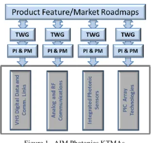
The Key Technology Manufacturing Areas (KTMAs) are structured to bring photonic integration needs from different market application segments, and thus function like “business units” in a corporation. Their charter is to select market-driven demonstrator projects that serve as drivers to advance AIM Photonics manufacturing capability. To achieve this each KTMA has a dedicated Technical Working Groups (TWGs) comprised of institute partners for inputs and project proposals, and each KTMA has industry, government, and academic co-leads. The KTMAs are illustrated in Figure 1, and today four have been identified:
1. Very High Speed Data and Communications 2. RF and Analog Photonics
3. Integrated Photonics Sensors 4. PIC Arrays Technologies
VHS Digital Data and Comm. Links Analog and RF I Communications Integrated Photon ic Sensors II PIC Array Technologies
Test, Assembly &
Packaging (TAP) r's
A9anuf cturing innovation
Centers+rzf E]aellent(R4CEgf
Electronic & Photonic Design Automation (EPDA)
MultiProject Wafer
& Assembly (MPWA)
Infine Control &Test (ICI) Figure 1. AIM Photonics KTMAs.
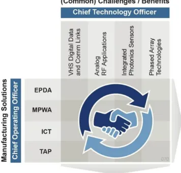
The Manufacturing Innovation Centers of Excellence (MCEs) provide the infrastructure and talent to both develop advanced manufacturing solutions and also provide baseline capabilities in each manufacturing support area. The MCEs thus function in a manner similar to the manufacturing and design platforms in a corporation, and they form the backbone for executing the AIM Photonics manufacturing mission. The MCEs also use dedicated TWGs comprised of institute partners to provide project inputs, and the enterprises represented in these TWGs also often comprise the fabric to execute the development and provision of prototyping capability for the institute. The MCE TWGs also have an industry, government, and academic co-lead. There are four MCEs, as illustrated in Figure 2:
1. Electronic and Photonics Design Automation (EPDA) 2. Multi-Project Wafer and Assembly (MPWA)
3. Inline Control and Test (ICT) 4. Test, Assembly and Packaging (TAP)
Figure 2. AIM Photonics MCEs.
Manufacturing Solutions Chief Operating Officer E D D F)
*
- a --1 D m -o 0 DVHS Digital Data and Comm Links Analog RF Applications Integrated Photonics Sensors Phased Array Technologies
To facilitate the goals of AIM Photonics the KTMAs and MCEs function together in a matrix as illustrated in Figure 3 below, with the KTMAs coordinated by the Chief Technical Officer and the MCEs coordinated by the Chief Operating Officer:
Figure 3. AIM Photonics Matrix Operations.
2. MANUFACTURING ECOSYSTEM
2.1 Advancing the Manufacturing EcosystemAs noted in Section 1.1, one of the goals of AIM Photonics is to emulate the dramatic successes experienced by the electronics industry over the past 40 years and transition key lessons, processes, and approaches to the photonic integrated circuit industry. The matrix structure described above provides a powerful vehicle to help drive industry manufacturing advances and the maturation of the ecosystem.
One of the lessons learned is the power of stratification of the ecosystem. Rather than championing the continued dominance of large, vertically integrated efforts, AIM Photonics seeks to encourage the development of industry partners, or teams formed within the MCE TWGs, that are specialized in their MCE ecosystem segment to generate and offer solutions with functionalities that benefit a broad array of applications.
The MCEs of AIM photonics are specifically chosen to encourage this stratification. As a specific example, partner companies who specialize in offering electronic and photonic design automation (EPDA) solutions can benefit by participating in the institute to understand both the rapidly developing wafer, test, and packaging technologies and the market applications that are likely to be driving the use of their future products. Early versions of products can be developed and vetted within this community, benefiting both the EPDA vendors and the leading-edge applications companies developing market applications of integrated photonics.
Similarly, the MPWA MCE provides a venue to drive advances in materials integration, process and wafer-scale assembly processes, and support high-performance devices, circuits and functional block libraries in cooperation with EPDA to benefit a broad spectrum of applications.
It is the job of the Chief Operating Officer and the MCEs to identify synergistic investments that most broadly serve the sometimes-diverse market needs of the different KTMAs. Thus, in addition to provide baseline foundry services, the
MCEs will often be pressured to support specialized projects for each KTMA. Because the goal of AIM Photonics is to drive the development of volume manufacturing solutions, in many cases if this synergy is not present or anticipated, the MCE may elect to not support the project through shared funding resources. The remaining alternative remaining is for the entire support for a narrowly-impacting manufacturing support capability to be born entirely by a corporate and/or government sponsor, and then only if capacity and resources are available.
One area where this synergy development is exceptionally challenging is in the Test, Assembly and Packaging (TAP) MCE. This is partly because the final system-level packaging is where a high-degree of market-driven product customization takes place, working against the concept of reference solutions. Additionally, customer-specific functional customization is where many of the more proprietary features are incorporated, also working against the concept of standardization.
AIM Photonics seeks to partially mitigate these challenges by partitioning the packaging into two levels. The first level is the generation of chip-stack subsystems, while the second level is the conversion of these chip-stack subsystems into product-specific solutions with system-level packaging. The first of these is supported primarily by the MPWA MCE function, while the second is supported primarily by the TAP MCE function.
This strategy is based on a belief that a large volume benefit can be achieved with wafer-scale assembly processes, where a variety of integrated photonic and integrated electronic wafer/chip solutions can strongly leverage advances in VLSI manufacturing infrastructure being driven by today’s volume markets. Specific examples of this include 3D wafer and chip-stacking manufacturing assembly technologies being driven by consumer markets in memory, imaging systems, and even functional processor/memory stacks. The principal here is that these advances are only affordable due to the associated volume markets, and integrated photonics markets need to adopt these manufacturing methods with minimal change, and hence minimal customization. Customization at this level comes primarily from the design of the chip-stack elements – i.e., the integrated photonics circuit and electronics themselves – rather than the assembly process. For the system-level packaging, AIM Photonics seeks to find synergies by advancing the application and adoption of more common toolsets in the manufacture of final product configurations. This can be partly facilitated by common interface features of chip-stack subassemblies, but also by providing a venue where product designers can make balanced judgments regarding the cost and time-to-market benefit of adopting commonality in solutions where they do not seriously compromise customer-desired features.
3. MANUFACTURING ADVANCE EXAMPLES
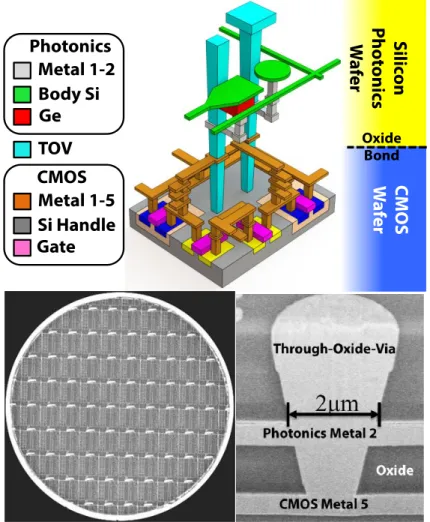
3.1 Examples of Manufacturing AdvancesIn this section several examples will be provided of manufacturing advances that AIM Photonics intends to pursue. One of these, already alluded to in the packaging discussion above, is the 3D stacking of photonics and electronics to provide functional chip-stack subassemblies as deliverables from the MPWA foundry services – and hence the inclusion of the “A” for “Assembly” in addition to the more common Multi-Project Wafer.
Work illustrating this capability has already been demonstrated by AIM Photonics members from MIT and SUNY Polyatechnic and UC Berkeley[1] and is illustrated in Figure 4 below. This wafer-scale CMOS-Silicon Photonics stacking was able to achieve Through-Oxide-Via (TOCV) face-to-face bonding with only ~1-to-2fF capacitance per contact, and pitch density of ~3μm with contact yields already > 99.999%. Using this advanced manufacturing technology, the team was able to demonstrate the lowest power silicon photonic communication link to date at 250fJ/bit. Another goal of AIM photonics EPDA MCE is to provide foundry users with the ability to co-design CMOS and Silicon Photonics, and then through the MPWA MCE take delivery of chip-stack subassemblies such as those illustrated above. Other powerful technologies being targeted include compound semiconductor integration. These range from full InP-based PIC development into new applications, to heterogeneous bonded InP/silicon photonics, to direct compound semiconductor epitaxy on silicon photonics. These technologies are being developed by AIM Photonics partner companies including Infinera, Aurrion, and Intel, in addition to UC Santa Barbara where promising epitaxial approaches have recently been demonstrated[2].
Through-Oxide-Via
Photonics Metal 2
CMOS Metal 5
maimooreasommeesuosemess
The authors would like to acknowledge, and express their gratitude to, the US Department of Defense ManTech program, participating state governments, and corporate partners for their cooperative support of AIM Photonics. The views and conclusions contained herein are those of the authors and should not be interpreted as necessarily representing the official policies or endorsements, either expressed or implied, of Air Force Research Laboratory or the U.S. Government.
REFERENCES
[1] Timurdogan, E., Su, Z., Settaluri, K., Lin, S., Moazeni, S., Sun, C., Leake, G., Coolbaugh, D. D., Benjamin R. Moss, B. R., Moresco, M., Stojanović, V., and Watts, M. R. “An Ultra Low Power 3D Integrated Intra-Chip Silicon, Electronic-Photonic Link,” in Optical Fiber Communication Conference Post Deadline Papers, OSA Technical Digest (online) (Optical Society of America, 2015), paper Th5B.8.
[2] Liu, A. Y., Zhang C., Norman, J., Snyder, A., Lubyshev, D., Fastenau, J.M., Liu, A. W. K., Gossard, A. C., and Bowers, J. E., “High performance continuous wave 1.3μm quantum dot lasers on silicon,” Appl. Phys. Lett. 104, 041104 (2014)
Figure 4 Top: Stacked architecture of silicon photonics circuit wafer placed above CMOS wafer with TOV ultra-low capacitance TOV interconnect. Bottom Left: Full 300mm stacked wafer plan view. Bottom Right: SEM of TOV plug illustrating 1-2um dimensions.