HAL Id: hal-00954424
https://hal.archives-ouvertes.fr/hal-00954424
Submitted on 4 Mar 2014
HAL is a multi-disciplinary open access
archive for the deposit and dissemination of
sci-entific research documents, whether they are
pub-lished or not. The documents may come from
teaching and research institutions in France or
abroad, or from public or private research centers.
L’archive ouverte pluridisciplinaire HAL, est
destinée au dépôt et à la diffusion de documents
scientifiques de niveau recherche, publiés ou non,
émanant des établissements d’enseignement et de
recherche français ou étrangers, des laboratoires
publics ou privés.
temperature local probing and noise
Claude Chapelier, F. Lefloch, Hervé Courtois, Klaus Hasselbach
To cite this version:
Claude Chapelier, F. Lefloch, Hervé Courtois, Klaus Hasselbach. Hybrid superconducting
nanos-tructures: very low temperature local probing and noise. International Journal of Nanotechnology,
Inderscience, 2010, 7 (4-8), pp.456-473. �10.1504/IJNT.2010.031730�. �hal-00954424�
Hybrid superconducting nanostructures: very low
temperature local probing and noise
C. Chapelier and F. Lefloch
INAC-SPSMS, CEA Grenoble,
17 avenue des martyrs, 38042 Grenoble, France E-mail: claude.chapelier@cea.fr
E-mail: francois.lefloch@cea.fr
H. Courtois* and K. Hasselbach
Institut Néel,
CNRS and Université Joseph Fourier,
25 avenue des martyrs, 38042 Grenoble, France E-mail: herve.courtois@grenoble.cnrs.fr
E-mail: klaus.hasselbach@grenoble.cnrs.fr *Corresponding author
Abstract:We review the topic of hybrid superconducting nanostructures by introducing the basic physical concepts and describing recent key experimental results. We discuss the superconductivity nucleation in mesoscopic structures, the vortex lattice imaging in doped diamond films, the superconducting proximity effect, multiple Andreev reflection in Josephson junctions and the electronic micro-cooling in hybrid tunnel junctions. An emphasis is put on very low temperature local probes and noise measurement techniques developed in Grenoble.
Keywords: near-field microscopy; tunnelling; vortex; micro-cooling; mesoscopic superconductivity; Andreev reflection; noise.
Reference to this paper should be made as follows: Chapelier, C., Lefloch, F., Courtois, H. and Hasselbach, K. (2010) ‘Hybrid superconducting nanostructures: very low temperature local probing and noise’,Int. J. Nanotechnol., Vol. 7, Nos. 4/5/6/7/8, pp.456–473.
Biographical notes:Claude Chapelier is a staff member at CEA-Grenoble. His PhD Thesis (1989) focused on phonons in superfluid helium. Then, he worked in CNRS (Grenoble) where he has been involved in Mesoscopic Physics and Persistent currents in normal metal rings. In 1993 and 1994, he designed and built a low temperature UHV STM in Lawrence Berkeley Laboratory (USA). Since 1995, he developed a very low temperature STM in CEA-Grenoble. His recent research activities deal with STM spectroscopy of non-uniform superconducting systems such as highly disordered superconducting thin films, hybrid superconducting nanostructures and magnetic vortex in type II superconducting films.
François Lefloch is engineer-physicist at the CEA-Grenoble-INAC in the Service of Statistical Physics, Magnetism and Superconductivity (SPSMS). After a PhD at CEA-Saclay (spin glass dynamics) and two years post-doc at UCLA (NRM response and vortex motion), he reached the CEA-Grenoble in 1995. His main research activity focuses on noise measurements in multi-terminal superconducting hybrid nanostructures and more generally in quantum electronic transport in nanostructures. Since 2006, he is the deputy head of the SPSMS.
Hervé Courtois is Professor at Université Joseph Fourier (UJF) since 2005 and member of the Institut Universitaire de France. His research activity at Institut Néel – CNRS and UJF covers the proximity effects between metals and superconductors, Josephson junctions and electronic cooling. This has led him to develop innovative very low-temperature local probe microscopes (STM and combined AFM-STM). Since 2005, he is the director of the European School On Nanosciences and Nanotechnologies (ESONN, www.esonn.fr).
Klaus Hasselbach is Director of Research (CNRS), PhD University Karlsruhe 1991, Germany, World Trade Post-doctoral Fellow at IBM T.J. Watson Research Lab, 1992. His research activities concern nanomagnetism, superconductivity and scanning probe microscopy. He has developed a novel scanning nano- SQUID microscope working at very low temperature.
1 Introduction
Superconductivity is a macroscopic quantum state, whose signature is zero dc-resistance and complete diamagnetism. Diamagnetism is achieved by screening currents at the surface of the sample nulling the applied field in the sample (Meissner-Ochsenfeld effect). Superconductivity sets in upon lowering of temperature as the formation of pairs of electrons allows to diminish their energy. The pairs of electrons are called Cooper pairs and consist of two undistinguishable electrons of opposite spin and momentum. Two length scales characterise superconductivity, first the coherence length, ξ, a length corresponding to the spatial extent of a Cooper pair and the penetration depth, λ, the width the superconducting screening currents need to shield the field. When a magnetic field is applied to a superconductor, it interferes in many ways with superconductivity. The quantum state wavefunction acquires a phase factor, via the vector potentialA, resulting in a space-dependent free energy Ginzburg-Landau functional. If the ratio of λ/ξ is smaller than 1/√2, a coexistence of normal and superconducting regions is observed. The regions have typically length scales of several micrometres, these materials are called type I superconductors and are mostly elemental superconductors. If the ratio λ/ξ is larger than 1/√2, it is energetically favourable for the material to admit magnetic flux in a quantised manner. These flux quanta are called vortices and contain a flux Φ0= h/2e = 2.06 × 10⁻¹⁵Wb with h being
Planck’s constant and e the charge of the electron. At its centre in a region of diameter of ξ, each vortex contains unpaired electrons. When the field rises above
a first critical field Hc1, vortices begin to penetrate the centre of the sample and
superconductivity weakens. Due to a repulsive interaction between them, the vortices arrange themselves in a triangular array (Abrikosov array) which can be more or less distorded depending on the density of pinning centres created by chemical or structural disorder in the material. Superconductivity disappears in the bulk when the vortices cores overlap at a field Hc2, and also from the surface sheath at a
fieldHc3= 1.7 Hc2. BetweenHc2 andHc3, the superconducting sheath has a typical
width of the order of the coherence length [1]. The superconductivity vanishes last and appears first at the surface, due to the wavefunction’s boundary condition of zero transverse amplitude at this place.
When a superconductor is in contact with a normal metal, single electrons are transformed in Cooper pairs and vice versa continuously. At theN/S interface, the microscopic mechanism is the Andreev reflection of an electron into a hole, which traces back almost exactly the trajectory of the incident electron. This coherent process corresponds to the transfer of a Cooper pair in S and its inverse to the diffusion of an electron Andreev pair in the normal metal [2]. In the vicinity of the interface, the diffusion of Andreev pairs induces superconducting-like physical properties in the normal metal. One aspect of this so-called proximity effect is the local modification of the energy spectrum. In the case of a N/S junction with a normal metal of finite length, the density of states in N is expected to exhibit a mini-gap: the density of states is zero within an energy window around the Fermi level. The width of this mini-gap is smaller than the intrinsic superconducting gap of the superconductor. In the case of a normal metal with an infinite length, the density of states will exhibit a pseudo-gap: the density of states is zero only at the exact Fermi level and goes approximately linearly with the energy close to the Fermi level. This behaviour can be understood by arguing that some electron trajectories travelling close to the interface never hit it, therefore do not couple to superconductivity and contribute to the density of states. Practically, the criteria of an infinite length for the normal metal should be understood as a length larger than the phase coherence length. In every case, the characteristic energy scale is given by the Thouless energyETh= !D/L2whereD is the diffusion coefficient and L is the
size of the metal or the distance from the interface.
If two superconductors are connected to a short normal metal (S/N/S junction) [3], a dissipationless supercurrent can flow. Here, we consider a length of the normal bridge smaller than the phase coherence length Lφ of the normal
metal and transparent contacts between the superconducting electrodes and the normal metal. A case of particular interest deals with long junctions defined by a junction lengthL larger than the induced superconducting coherence length in the normal metal ξN but still smaller than the single particle coherence length Lφ, in
contrast with the short junction case L < ξN met for instance in superconducting
atomic point-contacts. In a long S/N/S junction, the Thouless energy ETh=
!D/L2 is smaller than the gap ∆ and it determines the amplitude of the maximum supercurrent. At finite voltage, the charge transport though aS/N/S junction occurs mainly through Multiple Andreev Reflections (MAR): normal metal quasiparticles with an energy #< ∆ go through successive Andreev reflections at the two N/S interfaces until they reach the superconducting gap energy ∆. With an applied biasV , the number of successive MAR is equal to 2∆/eV + 1. Thus, two regimes can be met depending on the voltage bias. At low bias, the electron and hole trajectories coincide and multiple charge quanta are coherently transferred through
the S/N/S junction. In the (high-bias) incoherent regime eV > ET h, the electron
and the hole have, away from the interface, independent trajectories. The electronic transport then occurs by incoherent MAR, which induce excess noise as compared to a similarN/N/N system.
2 Superconductivity nucleation in mesoscopic structures
Two experimental set-ups described below, Scanning Tunnelling Microscopy (STM) and Scanning nano-SQUID Microscopy (SnSM), can probe, in different ways, inhomogeneous superconducting states, such as the mixed state of a type II superconductor. In the case of STM, this is the signature in the LDOS of the zeroing of the order parameter which is probed whereas in the case of SnSM, this is the local magnetic field.
2.1 Magnetic microscopy
As an applied magnetic field induces a modulation of the superconducting state and notably the appearance of vortices, magnetic microscopy is a tool of choice to observe the inhomogeneous magnetic state of a superconductor. One way to do this is to scan a microscopic flux meter above the surface of the superconductor. A very sensitive flux-meter is the Superconducting Quantum Interference Device (SQUID). The direct current (dc)-SQUID consists of a superconducting loop with two Josephson junctions.
When a magnetic flux Φ threads this superconducting loop, a circular supercurrent is induced which is periodic with Φ with a period equal to Φ0. The
presence of such a supercurrent decreases the maximal dissipationless dc-current one can drive across the SQUID. As a result, this critical currentIcis also a Φ0-periodic
function of the applied magnetic flux. The measurement of Ic(Φ, x, y) for each
position (x, y) of the nanoSQUID above the sample surface gives a direct access to the local variations of the magnetic field. For instance, for a SQUID loop area of 1 µm2
a periodic modulation of Ic corresponds to a field variation of 2.06 mT.
Such a nanoSQUID is well suited for detecting the magnetic field of a vortex in a type II superconducting film in the mixed state. Indeed, such a field can be estimated asH ≈ Φ0/2πλ2≈ 30 mT for a penetration depth λ of the order 100 nm. However
this is an upper limit of H, since it rapidly decreases when one moves away from the surface.
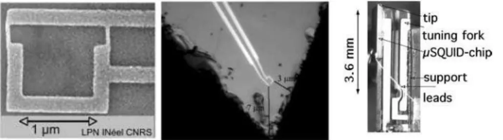
We have chosen to aim at high spatial magnetic resolution and adopted the nanoSQUID design based on Dayem bridges as Josephson junctions patterned by electron beam lithography see Figure 1 [4]. The bridges have a width of the order of 20 nm. Microscopes based on bigger and more sensitive SQUID [5] are described in literature, though their spatial resolution is lesser and their design far more complex. At a height of 1 µm above the surface, the field is reduced to about 1% of the estimated field in the centre of the sample. This rapid decrease of the field amplitude as a function of the distance between the nanoSQUID and the sample surface means that close proximity between sample surface and nanoSQUID has to be maintained. We have chosen to implement an active height regulation between the sample and the nanoSQUID tip in attaching the nanoSQUID on a piezoelectric Quartz tuning
fork [6], see Figure 1. As the tuning fork is excited by a dither piezo ceramic, its resonance frequency which depends on the sample-SQUID distance is tracked by a phase locked loop controller. Any frequency shift is then used in a feedback loop to maintain this distance constant while scanning, in a similar way as in force microscopy. Such a scanning nanoSQUID force microscope has been integrated in a reversed dilution refrigerator, allowing imaging at very low temperatures.
Figure 1 Left: SEM image of a nanoSQUID of1µm diameter made of Aluminum, the two Josephson junctions are realised by 20 nm wide Dayem Bridges. Centre: The nanoSQUID placed at the very edge of the Si chip, Right: The sensor of the SQUID force microscope, tuning fork assembled with the nanoSQUID chip
The strength of low temperature high resolution magnetic imaging relies on the possibility to follow in situ the evolution of the magnetic structure of a superconductor upon changes in temperature and field. We applied this approach to the study of the vortex arrangements in a patterned array of holes in an aluminium film [7]. We chose aluminium because of its long coherence length and in consequence the weak vortex pinning effects. Aluminium behaves as a type-II superconductor if the thickness of the film is of the order of the penetration depth, and if the lateral dimensions are much larger than the thickness. The holes were arranged in a repetitive pattern of lines and each line was made of holes of either 0.5, 1 or1.5 µm diameter. The distance between the holes was 10 µm. Upon cooling in an applied field, due to the boundary conditions of the superconducting wave-function, the first regions that become superconducting are the regions at the borders of the sample and of the holes. When the edge of an hole becomes superconducting, the wave-function must be 2π periodic around the hole. As a consequence, the flux through the hole is quantised in 1, 2, or 3 Φ0, the quantification being possible due to
circulating screening currents in the superconductor around the holes. Figure 2(b) is taken at a field of 0.2 G, which is the matching field so that each hole carries exactly one flux quantum. The temperature at a given field for which the surface of each hole becomes superconducting depends on the hole curvature. The smaller the curvature, the closer the temperature gets to the bulk critical temperature. This size dependence is clearly visible in Figure 2(c). Upon field cooling, the flux passes through the bigger holes and the screening currents are set up to establish the 2π periodicity of the wavefunction around these holes. If no flux is left over, no screening currents will appear when the smaller holes become superconducting at lower temperatures. In this image, the site of the smallest hole remain dark: there are no screening currents.
Figure 2 Left: the film is patterned by holes of three diameters 0.5, 1 and1.5µm, each 10µm apart, on the images the holes of identical diameter are aligned on diagonals. Centre: scanning NanoSQUID Microscopy (SnSM) image 28µm × 28µm with 0.2 G field cooled to 0.4 K. Screening currents appear at each hole, 0.2 G is the amplitude of the first matching field. Right: SnSM image 28µm × 28µm with 0.14 G field cooled to 1.16 K. The diagonal of the smallest holes stays void of flux (superconducting regions are dark) (see online version for colours)
When the film is cooled in an applied field higher than the first matching field, interstitial vortices appear between the holes, as in Figure 3(a) where the field was 1.14 G. These ‘Abrikosov’ vortices nucleate preferentially at defects bigger than the vortex coherence length and stay more or less pinned at their position, as long as the coherence length stays shorter than the defect size. When the sample is warmed up close to Tc, here 1.18 K, the coherence length in Al starts to diverge and the
vortices become mobile, see Figure 3(b). At the same time, the penetration depth λ diverges also and the vortices become magnetically larger and the repulsion between the vortices diminishes. In Figure 3(b), it becomes apparent that the interstitial vortices are pushed together by the screening currents that circulate around the holes. In average, each vortex cloud between the holes is constituted of four vortices. When the temperature is raised even more, a new state appears. Localised superconductivity is visible around the larger holes of 1 and 1.5 µm diameter, the superconducting surface sheath persists above Hc2 as it is governed by Hc3(r) [8],
r being the curvature of the hole, Figure 3(c). This is the first direct observation by an imaging technique of the state of localised superconductivity.
Figure 3 (a) Scanning NanoSQUID Microscopy (SnSM) image28µm × 28µm field cooled to 0.4 K at 1.14 G. Interstitial Abrikosov vortices and the vortices due to the screening currents around the holes are undistinguishable; (b) at 1.18 K the interstitial Abrikosov vortices become mobile and caged in groups of about 4 vortices by the screening currents around the holes and (c) at 1.2 K the region around the diagonal of the smallest holes is filled by flux (bright: normal state), the circular regions around the larger holes are still superconducting (dark), which is an evidence for localised superconductivity (see online version for colours)
2.2 STM at low temperature
Scanning Tunnelling Microscopy (STM) provides highly resolved images of surfaces, making individual atoms visible. It can also provide a local spectroscopy of the electronic properties of nano-objects with atomic scale resolution. The Grenoble very low temperature STMs work at about 60 mK in a dilution refrigerator [9]. They feature both an atomic resolution and a large scanning range of6 × 6 µm2 at low
temperature. In the experiments described in this paper, the cryogenic environment is not only necessary because superconductivity and quantum coherence in nanostructures take place at very low temperature but also because the energy resolution in spectroscopy techniques, such as Scanning Tunnelling Spectroscopy (STS), improves when approaching zero temperature. In this limit, the tunnelling probability of an electron between the STM tip and the sample is simply proportional to the local electron density of states (LDOS) of the two materials integrated in a energy window eV , the energy shift of the Fermi levels of the two metals. In this energy range, all the electronic states which are fully occupied in one electrode can tunnel in fully empty states in the other one. The tunnelling current can therefore be written as
I(V ) = GT
! eV 0
νt(# − eV ) νs(#) d#, (1)
where νt(#) and νs(#) are the LDOS of the tip and the sample respectively and GT
a quantity proportional to the tunnelling conductance. Since characteristic energies for spectroscopy on superconducting samples at low temperature are in the meV range, one can assume further a constant LDOS for the tip when made from a normal metal. Then the differential tunnelling conductance becomes proportional to the LDOS of the sample at an energyeV :
dI
dV = GT e νt(0) νs(eV ). (2) However, at non-zero temperature, the Fermi-Dirac distributionf (E) influences the tunnelling current, which becomes temperature dependent.
I(V ) = GT νt(0) ! +∞ −∞ νs(#) [f (#) − f(# − eV )] d# (3) and dI dV = GT e νt(0) ! +∞ −∞ νs(#) ∂f ∂E d#. (4)
In the spectroscopy mode, the energy resolution of a tunnelling experiment is thus given by the thermal energy:3.5 kBT. Our STMs have shown an energy resolution
below36 µeV. One way to improve this resolution is to use a superconducting tip whose LDOS is peaked at the superconducting gap energy and acts as an additional energy filter.
The first picture of an Abrikosov array by STS has been obtained on NbSe2 [10,11]. Moreover, since this material is a clean superconductor (l % ξ, where
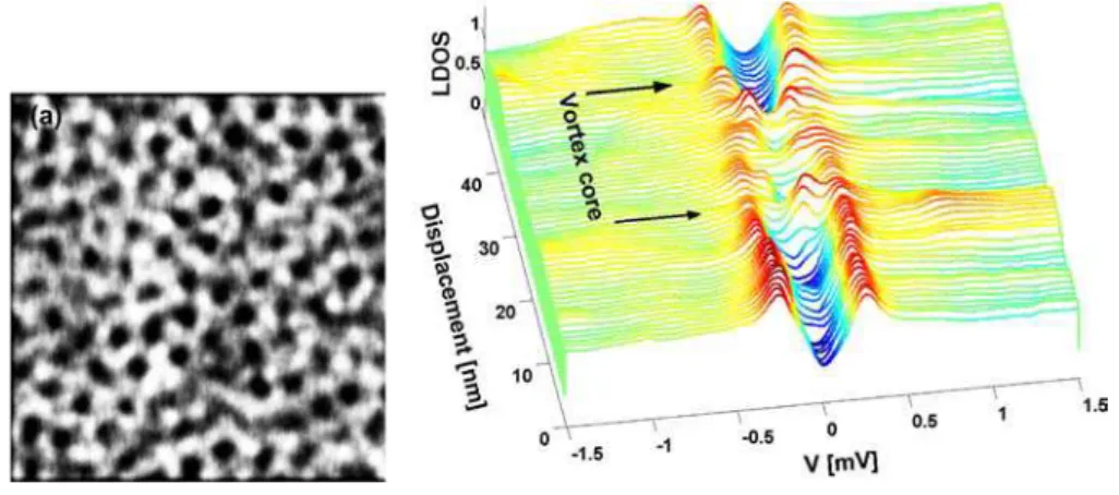
l is the mean free path), localised states in the core of the vortex have been observed. These states are similar to ballistic Andreev trajectories in shortS/N/S junctions. However in dirty superconductors (l & ξ), these trajectories mix up and one recovers a flat density of states in the vortex core [12]. We have visualised by STS the Abrikosov array in boron-doped diamond thin films [13–15]. These films become dirty superconductors material below a critical temperature of a few Kelvin, which depends on the doping level. Although the disordered triangular lattice could be observed (see Figure 4), the LDOS of the vortex core displayed a pseudogap which cannot be understood in the framework of standard metals. On the other hand, many resonant states in this pseudogap could be observed, in the vortex core but also in the vicinity of the vortex as well. The low density of electrons in this material is a possible clue for this anomalous behaviour.
Figure 4 Left: STM vortex picture1.5 × 1.5µm2
acquired below 100 mK and with a magnetic field of 1200 Oe on a boron-doped diamond film. The presence of vortices is revealed by a decrease of the differential conductance dI
dV. This yields
dark spots arranged on a disordered Abrikosov array. Right: tunnelling spectra acquired every 0.7 nm along a line crossing a vortex core which extends between the two arrows. Unexpected numerous localised resonances at non zero energies inside the gap are visible (see online version for colours)
3 The superconducting proximity effect
3.1 STM: Local Density of States
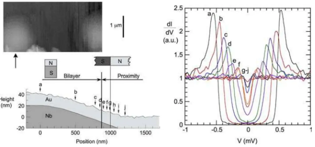
We have performed the local spectroscopy at 60 mK of a Nb/Au sample made of superconducting Nb dots with a rather smooth profile buried below a normal metal Au film [16]. We measured several series of spectroscopies as a function of distance from the centre of a Nb dot by travelling along one line. Figure 5 shows a representative selection of spectra taken during a single series. In the centre of the Nb island (curve a), the density of states exhibits a clear gap, which is reminiscent of a BCS behaviour. Compared to the bulk Nb gap value of '1.4 meV, the measured gap is significantly reduced due to inverse proximity effect. As we move away from the Nb dot centre (curves b to d), the density of states first continues to
exhibit a fully developed but reduced gap. This remains approximately true up to close to the curve e, which shows a clear pseudo-gap: the density of states goes approximately linearly to zero at the Fermi level. As the tip is moved further away (spectra e to j), the pseudo-gap width is reduced. We have been able to observe a pseudo-gap behaviour in the density of states spectra over about 300 nm. This experimental data compares favourably with the spectra calculated from the Usadel equations [16], assuming a very simple geometrical model of the complex sample geometry. In the bilayer region, we consider the sample as a bilayer with a varying Nb layer thickness. In the ‘proximity’ region, we consider a lateral N/S junction. From the fit parameters, we found that spin-flip and inelastic scattering could be neglected, which means that the related characteristic lengths should be larger than about 300 nm.
Figure 5 Right, top :2.6 × 5µm2
STM image at 60 mK captured with a 10 mV bias voltage and a 30 pA tunnel current. Two circular Nb dots are visible. Right, bottom: profile of the sample surface extracted from image (line indicated indicated by the arrow) together with a schematics of the sample geometry. Note that the vertical scale has been expanded by a factor of about 10 compared to the horizontal one. The locations where the spectra were measured are indicated, as well as the domains of application of the two geometry models used in the calculations. Left: experimental spectra measured on locations a to j during a single scan along one line (see online version for colours)
We have carried out a similar study in Nb/Au bilayers with an increased gap thanks to a larger thickness of the Nb layer [17]. This increased ∆/kBT enabled us to unveil
an anomalous behaviour of the local density of states at the surface: a non-zero density of states appears within the mini-gap and increases when the thickness of the Au layer is increased. This behaviour is presumably related to the shape of the Au Fermi surface.
3.2 Noise in S/N/S diffusive hybrid superconducting nanostructures
In this section, we describe recent results obtained on the noise in diffusiveS/N/S junctions. We have measured the current noise of junctions of various length from 0.4 µm to 0.8 µm. They are all based on aluminium – copper – aluminium contactsevaporated in situ through shadow masks. This ensures a very good electrical contact between the superconducting material (Al) and the diffusive metal (Cu).
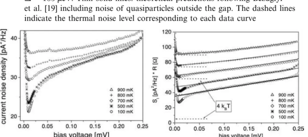
The overall behaviour of the current noise density as a function of bias voltage is shown in Figure 6. We observe a pronounced minimum atV ≈ 10 µV corresponding to the Thouless energy ETh' 7 µeV. This minimum indicates the transition from
the regime of coherent pairs transport at low voltage to the regime at higher voltage where the Andreev pairs are split off into independent quasiparticles before reaching the opposite interface. In this incoherent regime, the proximity effect can be neglected and the noise is given by:
SI(V ) =
1
32 eI × N = 2
3R(eV + 2∆). (5)
It corresponds to the zero temperature shot noise of a coherent diffusive normal metal sample times the number of Andreev reflections. This expression is exactly the prediction of semiclassical theory in the zero temperature limit and when no inelastic processes take place [18,19]. In our junctions however, proximity effect corrections persist over the whole voltage range. In order to take into account the related voltage dependence of the resistance, we usedR(V ) = V /I in equation (5) rather than the normal resistance RN and analysed the product SI(V )R(V )
(Figure 6). At T = 100 mK we obtain a very good agreement between experiment and equation (5), see Figure 6, in the range from50 µV up to the current induced transition at about 260 µV. At temperatures above 500 mK, the thermal noise of the quasiparticles outside the gap has to be taken into account. Along the lines of Bezuglyi et al. [19], we write the total noise as a sum of this thermal noise and the subgap noise. The fits obtained using the BCS temperature dependence of the superconducting gap show excellent agreement with the experimental data between 500 mK and 900 mK.
Figure 6 Left: current noise density of a diffusive Al/Cu/Al(S/N/S) junction as a function of the voltage drop across the junction for various temperatures. Right: current noise density times the resistanceR = V /I vs. bias voltage at various temperatures (the data curves are shifted successively by10 pA2
/Hz). Thick solid line: theoretical prediction in the zero temperature limit (equation (5)) with ∆ = 165µeV. Thin solid lines: theoretical predictions following Bezuglyi et al. [19] including noise of quasiparticles outside the gap. The dashed lines indicate the thermal noise level corresponding to each data curve
For small voltages (V < 50 µV) the experimental data show a nonlinear regime which extends down to its minimum at the Thouless energy. The simple model
used above to derive equation (5) supposes a ‘collisionless regime’, where the quasiparticles reach the gap without inelastic interactions. However at low voltage and finite temperature, the effective length of the junction for the multiple retroreflected particlesLeff = N L ∼ L∆/V exceeds the inelastic length Lin. In this
‘interacting regime’, electron-electron collisions interrupt the successive incoherent multiple Andreev reflections before the quasiparticles reach the gap. In the case of strong interaction, a Fermi distribution with an effective temperature Te is
restored [20,21].
Figure 7 shows the low voltage (V < 8 µV) part of the noise spectral density as a function of bias from 500 mK to 800 mK. These results have been obtained in a second set of samples of the same kind. We have focused on the temperature range where no hysteresis is present. The first striking result is the overall divergence of the noise at low bias for every temperature. The second important feature is the broad peak with a maximum between2 µV and 4 µV. When the temperature increases, it is less and less pronounced, moves to lower voltages and finally disappears around 800 mK. We analyse this peak in terms of a mixing between the ac-Josephson current IJ and the fluctuating current δIN generated by the junction through its non-linear
response. In such a situation, the voltage fluctuations S(ω) at low frequency are determined not only by the current fluctuations at the frequency ω, but also by those close to the Josephson frequency ωJand its harmonics. Under some assumption [22],
the low frequency noise can be written as
SImeas(0) = SI(0)(1 − η), (6)
where the coupling factor η accounts for the down mixing additional noise measured at low frequency. We obtained the coupling factor η from the measured quantitiesV and Rd by numerically differentiating Rd with respect to the calculated I.
We can then extract, from the measured noise, the intrinsic junction noiseSI(0) =
SImeas(0)/(1 − η), see Figure 7. For all the curves the broad peak has disappeared or,
at least, has been strongly reduced.
Figure 7 Left: current noiseSImeas vs. bias voltageV at several temperatures between
500 mK and 800 mK. Inset:SI at 500 mK up to120µV. The solid line is the
noise prediction due to incoherent MAR. Right: current noise
SI(0) = SImeas/(1 − η) vs. bias voltage V at several temperatures between
500 mK and 800 mK (Data are successively shifted by 100 pA2
/Hz for clarity). Lines are the calculated noise4kBT /(V /I). Inset: 1 − η vs. V at the same
Figure 7 shows that SI(0) exhibits a strong divergence at low voltage, which
cannot be described by the thermal noise of the normal resistance 4kBT /RN as in
Koch et al. [23]. We cannot either understand the data by introducing an effective temperature, as we would get an unrealistic effective temperature as high as 100 K. We thus propose that the low voltage noise writes as
SI(0) =
4kBT
V /I . (7)
The comparison with experimental data of SI(0) is shown in Figure 7 with no
adjustable parameter. Between 800 mK and 550 mK, the agreement is remarkable.
Equation (7) can be understood in two ways. First, it is the low voltage limit (eV & kBT ) of the quasiparticle noise of a junction with low transmitting channels:
SI(0) = 2eI coth(eV/2kBT ). If effective charges e∗> e are responsible for the
transport, e should be replaced by e∗
= Ne in the above expressions. In that case, the condition e∗
V = NeV & kBT for equation (7) to remain valid, is verified as
long as N < 30 at 1 µV and 550 mK. In this description, only channels with low transmission coefficients contribute to the current and to the noise. Equation (7) might also be related to the fluctuation – dissipation theorem in a non-linear system, in which the resistanceRN would be replaced by V /I(V ). Here, dissipation arises
from electron-electron interactions that necessarily occur at low voltage due to the large number of Andreev reflections needed for the quasiparticles to escape into the superconducting electrodes. In both cases, we conclude that, at very low voltage and ‘high’ temperature, the current noise in long S/N/S junctions is governed by the transport of incoherent quasiparticles between the two superconducting reservoirs, which induces a noise divergence when the voltage goes to zero [18].
When decreasing further the temperature, the experimental data present a large excess noise compared to equation (7) expression. Therefore, additional noise sources must be involved. It is worth noting that this deviation from a pure quasiparticles noise occurs below 525 mK, which corresponds to kBT ' 3.5 ETh,
very close to the mini-gap width (3.1 ETh) [22]. This suggests that coherent
processes, which become relevant in this energy scale, should play a role here.
4 Micro-cooling in hybrid devices
In a N-I-S tunnel junction (where I stands for Insulator), single quasi-particles can tunnel from the normal metal to the superconductor if their energy, as measured from the superconductor Fermi level, is larger than the superconducting gap. This energy selectivity induces a cooling of the electronic population of the normal metal in a S-I-N junction biased at a voltage below the gap ∆/e. As the heat current direction does not depend on the sign of the bias, S-I-N-I-S micro-coolers based on a double tunnel junction feature a double cooling power and an improved efficiency due to the better thermal isolation of the metal. The electronic temperature reduction reaches an optimum at a voltage bias just below the gap. In a Al-based device, normal metal electrons can cool from a bath temperature of 300 mK down to below 100 mK [24,25].
We have studied the electron transport properties of S-I-N-I-S electronic micro-coolers down to very low cryostat temperature (90 mK) [26]. A differential
conductance peak is observed at zero bias and identified as the contribution of the Andreev reflection to the sub-gap current, see Figure 8 left. As the temperature is decreased, this Andreev current increases, as it arises from the phase coherence in the normal metal. We have shown that the Andreev current introduces additional dissipation in the normal metal, equivalent to Joule heating. By analysing quantitatively the heat balance in the superconducting micro-cooler, we provide a full description of the evolution of the electronic temperature with the voltage. The dissipation induced by the Andreev current is found to dominate the single particle tunnelling-based cooling over a large bias range, see Figure 8 right. This newly uncovered contribution is thus of great importance for the analysis of the thermal behaviour of superconducting micro-coolers as well as of other hybrid devices.
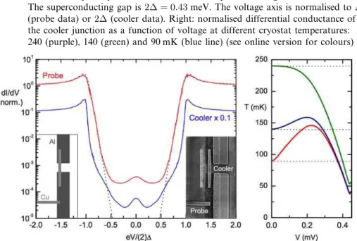
Figure 8 Left: differential conductances measured at a cryostat temperature of 90 mK. Top (red) curve: data of one probe junction1.55µm from the cooler junction and of normal-state resistanceRN= 2.76 kΩ. The black dotted line is a fit
describing the single quasi-particle tunnelling current. Bottom (blue) curve: cooler junction data with a normal state resistanceRN = 1.9 kΩ. Inset: schematics and
micrograph of a cooler made of two Al-AlO(x)-Cu junctions in series. The area of a cooler junction is1.5 × 0.3µm2
. In addition to the cooler, one of the three Al-AlOx-Cu probe junctions on the bottom superconducting electrode is visible.
The superconducting gap is2∆ = 0.43 meV. The voltage axis is normalised to ∆ (probe data) or2∆ (cooler data). Right: normalised differential conductance of the cooler junction as a function of voltage at different cryostat temperatures: 240 (purple), 140 (green) and 90 mK (blue line) (see online version for colours)
5 Conclusion and perspectives
The studies of hybrid superconducting nanostructures described in this paper offer new inroads into mesoscopic physics, nanoscale devices and low temperature experimental developments which provide the ground for ongoing researchs in Grenoble. Apart from unexpected observations in granular superconductors [27], proximity effect in diffusive systems is well understood, and many experiments
have been performed to investigate it on a mesoscopic scale [16,28,29]. Proximity effects in ballistic materials remains a difficult experimental challenge. However, a breakthrough can be done with the recent discovery of graphene [30]. This new material made of a single atomic layer of carbon atoms arranged on a hexagonal array is expected to allow ballistic transport on very long distances up to several microns. Moreover, because of a peculiar band structure, under certain circumstances, Andreev conversion of an electron into a hole and a Cooper pair is associated with a specular reflection. One can imagine devices where, by varying the Fermi level of graphene with the help of an electrostatic gate, the transfer of current between graphene and a superconductor can be tuned from a specular Andreev reflection into a usual retroreflection.
We have seen that inhomogeneous superconducting states can either be induced by a magnetic field or artificially tailored by lithography techniques. A third possibility is to weaken the superconductivity of a thin film by increasing its disorder. When impurities are incorporated or the film thickness reduced, the slow diffusion of the electrons impairs their ability to screen Coulomb repulsion, which competes with the attractive Cooper pairing. Ultimately, at a critical disorder and T = 0, a quantum transition happens, which drives the two-dimensional superconductor into an insulator. Although disorder can be made homogeneous down to a microscopic level, it is characterised by strong spatial fluctuations, like any statistical quantity. Close to the quantum superconductor-insulator transition but on the superconducting side, these spatial fluctuations induce an inhomogeneous superconducting state on a mesoscopic scale [31]. Many works are devoted to understand what kind of insulator can grow on this inhomogeneous superconducting state. Is it a Bose insulator where Cooper pairs still exist locally or is it a Coulomb glass with only electronic-like excitations? Local probes but also mesoscopic devices will probably shed light in a near future on these fundamental questions.
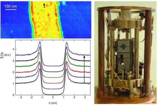
Requiring a metallic surface, STM is not well adapted for mesoscopic or nanoscopic structures built on insulating substrates. On the other hand, Atomic Force Microscopy (AFM) can image any kind of surface, but gives no information about electronic properties. We have developed a new kind of near field microscopy which combines force microscopy with tunnelling spectroscopy, working at very low temperatures [32]. This instrument, see Figure 9, can be used for near field studies of nanostructures with partly insulating surfaces. To achieve this, we use a piezo-electric tuning fork on which we make electrical contact with a glued tunnelling tip. The quartz tuning fork provides its natural rigidity to this hybrid probe, providing excellent stability for the tip in spectroscopic mode. The very low working temperatures achieved for this microscope (50 mK) guarantee very good energy resolution. We have studied the local superconducting properties for a sub-micron epitaxial wire of niobium on sapphire. The AFM image enabled us to localise the 8 nm high wire on the insulating sapphire surface. Once the point is positioned on the metal wire, the microscope is switched over to tunnelling mode to do local spectroscopy, measuring the variation of the density of electronic states with position. This new experimental approach opens new perspectives for the measurement of non-equilibrium effects in superconducting nanostructures.
Scanning nanoSQUID Microscopy has been successfully employed to study the magnetic state in crystals of unconventional superconductors [33,34]. Very often the
surface state of these materials is so delicate that STM techniques fail to access the electronic bulk state, but magnetic microscopy can detect vortex arrangements, and particular magnetic states, spontaneous currents etc. . . The nanoSQUID force microscopy has a huge potential of improvements: shaping tips by Si deep-etching in order to come closer to the surface and increase the magnetic flux-coupling, novel SQUID readout schemes . . . Several orders of magnitude can be won in spatial, magnetic and temporal resolution. This progress will allow to observe dynamic processes, and magnetic noise in superconducting quantum devices to name just a few new potentialities.
Figure 9 Top, left:115 × 950 nm2
AFM image of a 300 nm-wide Nb wire patterned on a sapphire substrate at 100 mK. Frequency shift is 0.15 Hz, tip oscillation
amplitude is 1 nm, scanning speed is 175 nm/s. Bottom: Differential conductance spectra acquired at 100 mK in units of the high bias conductance equals to 50 MΩ. The spectroscopies from bottom to top were acquired along a
25 nm-long displacement of the tip on the Nb wire as indicated by an arrow on the image. Right: Photograph of a very low temperature AFM-STM operating at 50 mK in a home-made upside-down dilution refrigerator. The motor stacks holding the sample are visible at the bottom and in front of the piezo-electric tube holding the tip (see online version for colours)
We have shown that current noise measurements provide a precise description of electronic transport in Josephson junctions. Having now a clear description of the current noise in diffusive S/N/S junctions and in diffusive S/N contacts [35,36], we are now addressing the problem of crossed correlations in multi-terminal superconducting hybrid nanostructures. The idea is to fabricate a normal nanostucture that is connected to one or several superconducting electrodes. If the nanostructure is small enough, an Andreev pair emitted by one superconducting electrode into the normal metal can split and one of the two quasiparticles
can propagate in one electrode connected to the nanostructure and the second quasiparticle in a different electrode. This crossed Andreev reflection process could be detected by crossed current correlations measurements. This would be the first step towards the fabrication and the detection of an electronic Einstein-Podolsky-Rosen (EPR) source [37] (and references therein).
Acknowledgements
The authors would like to acknowledge their collaborators P. Achatz, E. Bustarret, O. Coupiac, L. Crétinon, F. Dahlem, V. Dolocan, T. Dubouchet, W. Escoffier, P. Gandit, A.K. Gupta, N. Hadacek, F.W.J. Hekking, C. Hoffmann, D. Hykel, T. Klein, E. Lhotel, P.S. Luo, C. Marcenat, N. Moussy, F. Omnes, Z. Osvath, B. Pannetier, L. Pascal, T. Quaglio, S. Rajauria, B. Sacépé, M. Sanquer, J. Senzier, J-C. Villégier, A. Vasenko, C. Veauvy-Ladam, M. Vinet.
References
1 Fink, H.J. (1965) ‘Internal currents and magnetic fields close to the surface for a type-II superconductor for applied magnetic fields near the upper critical fieldHc2’,Phys. Rev.
Lett., Vol. 14, p.853.
2 Courtois, H., Gandit, P., Pannetier, B. and Mailly, D. (1999) ‘Long-range coherence and mesoscopic transport in N-S metallic structures’,Superlattices Microstruct., Vol. 25, Nos. 5–6, pp.721–732.
3 Dubos, P., Courtois, H., Pannetier, B., Wilhelm, F., Zaikin, A. and Schön, G. (2001) ‘The Josephson critical current in a long mesoscopic S-N-S junction’, Phys. Rev. B, Vol. 63, No. 6, p.064502.
4 Hasselbach, K., Veauvy, C. and Mailly, D. (2000) ‘Microsquid magnetometry and magnetic imaging’,Physica C, Vol. 332, p.140.
5 Kirtley, J.R., Ketchen, M.B., Stawiasz, K.G., Sun, J.Z., Gallagher, W.J., Blanton, S.H. and Wind, S.J. (1995) ‘High-resolution scanning SQUID microscope’,Appl. Phys. Lett., Vol. 66, p.1138.
6 Veauvy, C., Hasselbach, K. and Mailly, D. (2002) ‘Scanningµ-superconducting quantum interference device force microscope’,Rev. Sci. Instrum., Vol. 73, p.3825.
7 Veauvy, C., Hasselbach, K. and Mailly, D. (2004) ‘Micro-squid microscopy of vortices in a perforated superconducting Al film’,Phys. Rev. B, Vol. 70, p.214513, 5 pages. 8 Buzdin, A.I. (1993) ‘Multiple-quanta vortices at columnar defects’,Phys. Rev. B, Vol. 47,
p.11416.
9 Moussy, N., Courtois, H. and Pannetier, B. (2001a) ‘A very low temperature scanning tunnelling microscope for the local spectroscopy of mesoscopic structures’, Rev. Sci. Instrum., Vol. 72, No. 1, pp.128–131.
10 Hess, H.F., Robinson, R.B., Dynes, R.C., Valles, J.M. and Waszczak, J.V. (1989) ‘Scanning-tunneling-microscope observation of the Abrikosov flux lattice and the density of states near and inside a fluxoid’,Phys. Rev. Lett., Vol. 62, No. 2, p.214.
11 Hess, H.F., Robinson, R.B. and Waszczak, J.V. (1990) ‘Vortex-core structure observed with a scanning tunnelling microscope’,Phys. Rev. Lett., Vol. 64, No. 22, p.2711. 12 Renner, Ch., Kent, A.D., Niedermann, Ph., Fischer,Ø. and Lévy, F. (1991) ‘Scanning
tunnelling spectroscopy of a vortex core from the clean to the dirty limit’, Phys. Rev. Lett., Vol. 67, No. 12, p.1650.
13 Sacépé, B., Chapelier, C., Marcenat, C., Kaˇcmarˇcik, J., Klein, T., Bernard, M. and Bustarret, E. (2006a) ‘Tunneling spectroscopy and vortex imaging in boron-doped diamond’,Phys. Rev. Lett., Vol. 96, No. 9, p.097006.
14 Sacépé, B., Chapelier, C., Marcenat, C., Kaˇcmarˇcik, J., Klein, T., Omnes, F. and Bustarret, E. (2006b) ‘Experimental indications of a BCS behaviour in superconducting diamond’,Phys. Status Solidi A, Vol. 203, No. 13, p.3315.
15 Bustarret, E., Achatz, P., Sacépé, B., Chapelier, C., Marcenat, C., Ortega, L. and Klein, T. (2008) ‘Metal-to-insulator transition and superconductivity in boron-doped diamond’,Philos. Trans. R. Soc. A, Vol. 366, p.267.
16 Moussy, N., Courtois, H. and Pannetier, B. (2001b) ‘Local spectroscopy of a proximity superconductor at very low temperature’,Europhys. Lett., Vol. 55, No. 6, pp.861–867. 17 Gupta, A.K., Crétinon, L., Moussy, N., Courtois, H. and Pannetier, B. (2004)
‘Anomalous density of states in a metallic film in proximity with a superconductor’, Phys. Rev. B, Vol. 69, No. 10, p.104514.
18 Nagaev, K.E. (2001) ‘Frequency-dependent shot noise in long disordered-normal-metal-superconductor contacts’,Phys. Rev. Lett., Vol. 86, No. 14, p.3112.
19 Bezuglyi, E.V., Bratus, E.N.v., Shumeiko, V.S. and Wendin, G. (2001) ‘Current noise in long diffusive SNS junctions in the incoherent multiple Andreev reflections regime’, Phys. Rev. B, Vol. 63, No. 10, p.100501.
20 Hoss, T., Strunk, C., Nussbaumer, T., Huber, R., Staufer, U. and Schonenberger, C. (2000) ‘Multiple Andreev reflection and giant excess noise in diffusive superconductor/normal-metal/superconductor junctions’,Phys. Rev. B, Vol. 62, No. 6, p.4079.
21 Hoffmann, C., Lefloch, F. and Sanquer, M. (2002) ‘Inelastic relaxation and noise temperature in S/N/S junctions’,Eur. Phys. J. B, Vol. 29, No. 4, p.629.
22 Lhotel, E., Coupiac, O., Lefloch, F., Courtois, H. and Sanquer, M. (2007) ‘Divergence at low bias and down-mixing of the current noise in a diffusive superconductor-normal-metal-superconductor junction’,Phys. Rev. Lett., Vol. 99, No. 11, p.117002.
23 Koch, R.H., Van Harlingen, D.J. and Clarke, J. (1982) ‘Measurements of quantum noise in resistively shunted Josephson junctions’,Phys. Rev. B, Vol. 26, No. 1, p.74.
24 Giazotto, F., Heikkila, T.T., Luukanen, A., Savin, A.M. and Pekola, J.P. (2006) ‘Opportunities for mesoscopics in thermometry and refrigeration: physics and applications’,Rev. Mod. Phys., Vol. 78, No. 1, p.217.
25 Rajauria, S., Luo, P.S., Fournier, T., Hekking, F.W.J., Courtois, H. and Pannetier, B. (2007) ‘Electron and phonon cooling in a superconductor-normal-metal-superconductor tunnel junction’,Phys. Rev. Lett., Vol. 99, No. 4, p.047004.
26 Rajauria, S., Gandit, P., Fournier, T., Hekking, F.W.J., Pannetier, B. and Courtois, H. (2008) ‘Andreev current-induced dissipation in a hybrid superconducting tunnel junction’,Phys. Rev. Lett., Vol. 100, No. 20, p.207002.
27 Escoffier, W., Chapelier, C., Hadacek, N. and Villégier, M. (2004) ‘Anomalous proximity effect in an inhomogeneous disordered superconductor’, Phys. Rev. Lett., Vol. 93, No. 21, p.217005.
28 Vinet, M., Chapelier, C. and Lefloch, F. (2001) ‘Spatially resolved spectroscopy on superconducting proximity nanostructures’,Phys. Rev. B, Vol. 63, No. 16, p.165420. 29 Escoffier, W., Chapelier, C. and Lefloch, F. (2005) ‘Ballistic effects in a proximity
induced superconducting diffusive metal’,Phys. Rev. B, Vol. 72, No. 72, p.140502(R). 30 Novoselov, K.S., Geim, A.K., Morozov, S.V., Jiang, D., Zhang, Y., Dubonos, S.V.,
Grigorieva, I.V. and Firsov, A.A. (2004) ‘Electric field effect in atomically thin carbon films’,Science, Vol. 306, p.666.
31 Sacépé, B., Chapelier, C., Baturina, T.I., Vinokur, V.M., Baklanov, M.R. and Sanquer, M. (2006) ‘Disorder-induced inhomogeneities of the superconducting state close to the superconductor-insulator transition’, Phys. Rev. Lett., Vol. 101, No. 15, p.157006.
32 Senzier, J., Luo, P.S. and Courtois, H. (2007) ‘Combined scanning force microscopy and scanning tunnelling spectroscopy of an electronic nanocircuit at very low temperature’, Appl. Phys. Lett., Vol. 90, No. 4, p.043114.
33 Dolocan, V.O., Veauvy, C., Servant, F., Lejay, P., Liu, Y., Mailly, D. and Hasselbach, K. (2005) ‘Observation of vortex coalescence in the anisotropic spin-triplet superconductor Sr2RuO4’,Phys. Rev. Lett., Vol. 95, p.97004.
34 Dolocan, V.O., Lejay, P., Mailly, D. and Hasselbach, K. (2006) ‘Observation of two species of vortices in the anisotropic spin-triplet superconductor Sr2RuO4’,Phys. Rev. B,
Vol. 74, p.144505.
35 Jehl, X., Sanquer, M., Calemczuk, R. and Mailly, D. (2000) ‘Detection of doubled shot noise in short normal-metal/superconductor junctions’,Nature, Vol. 405, p.50.
36 Lefloch, F., Hoffmann, C., Sanquer, M. and Quirion, D. (2000) ‘Doubled full shot noise in quantum coherent superconductor-semiconductor junctions’, Phys. Rev. Lett., Vol. 90, p.067002.
37 Duhot, S., Houzet, M. and Lefloch, F. (2009) ‘Cross correlation of incoherent multiple Andreev reflections’,Phys. Rev. Lett., Vol. 102, p.086804.