Publisher’s version / Version de l'éditeur:
Journal of Vacuum Science and Technology A, 20, 3, pp. 1145-1148, 2002
READ THESE TERMS AND CONDITIONS CAREFULLY BEFORE USING THIS WEBSITE. https://nrc-publications.canada.ca/eng/copyright
Vous avez des questions? Nous pouvons vous aider. Pour communiquer directement avec un auteur, consultez la première page de la revue dans laquelle son article a été publié afin de trouver ses coordonnées. Si vous n’arrivez pas à les repérer, communiquez avec nous à [email protected].
Questions? Contact the NRC Publications Archive team at
[email protected]. If you wish to email the authors directly, please see the first page of the publication for their contact information.
NRC Publications Archive
Archives des publications du CNRC
This publication could be one of several versions: author’s original, accepted manuscript or the publisher’s version. / La version de cette publication peut être l’une des suivantes : la version prépublication de l’auteur, la version acceptée du manuscrit ou la version de l’éditeur.
For the publisher’s version, please access the DOI link below./ Pour consulter la version de l’éditeur, utilisez le lien DOI ci-dessous.
https://doi.org/10.1116/1.1467358
Access and use of this website and the material on it are subject to the Terms and Conditions set forth at
Characterization of thin ZrO2 films deposited using Zr(Oi-Pr)2(thd)2 and
O2
Chen, H. -W.; Landheer, D.; Wu, X.; Moisa, S.; Sproule, G. I.; Chao, T. -S.;
Huang, T. -Y.
https://publications-cnrc.canada.ca/fra/droits
L’accès à ce site Web et l’utilisation de son contenu sont assujettis aux conditions présentées dans le site LISEZ CES CONDITIONS ATTENTIVEMENT AVANT D’UTILISER CE SITE WEB.
NRC Publications Record / Notice d'Archives des publications de CNRC:
https://nrc-publications.canada.ca/eng/view/object/?id=a358318c-5156-4fa5-841c-5afe1dee7069 https://publications-cnrc.canada.ca/fra/voir/objet/?id=a358318c-5156-4fa5-841c-5afe1dee70692 2 2
and O
2on Si„100…
H.-W. Chena)Institute of Electronics Engineering, National Chiao-Tung University, Hsinchu 300, Taiwan, Republic of China
D. Landheer, X. Wu, S. Moisa, and G. I. Sproule
Institute for Microstructural Sciences, National Research Council of Canada, Ottawa, Ontario K1A OR6, Canada
T.-S. Chaob)
Department of Electrophysics, National Chiao-Tung University, Hsinchu 300, Taiwan, Republic of China
T.-Y. Huangb)
National Chiao-Tung University, Hsinchu 300, Taiwan, Republic of China
~Received 9 August 2001; accepted 11 February 2002!
The properties of ZrO2films deposited using molecular oxygen and a recently developed precursor,
zirconium Zr(Oi– Pr)
2(thd)2 have been investigated. The organometallic was dissolved as a 0.15
molar solution in octane and introduced into the deposition chamber using a liquid injection system. The deposition rate was insensitive to molecular oxygen flow but changed with liquid injection rate and was thermally activated in the range 390 °C–550 °C. Carbon concentrations, ,0.1 at. %, the detection limit of the x-ray photoelectron spectroscopy depth profiling measurements, were obtained at the lowest deposition temperatures and deposition rates. High-resolution transmission electron microscopy showed the films to be polycrystalline as deposited, with a zirconium silicate interfacial layer. After proper annealing treatments, an equivalent oxide thickness ~EOT! of around 2.3 nm has been achieved for a 5.2 nm thick film, with a leakage current two orders of magnitude lower than that of SiO2with the same EOT. Promising capacitance–voltage characteristics were also achieved,
but some improvements are required if these films are to be used as a gate insulator. © 2002
American Vacuum Society. @DOI: 10.1116/1.1467358#
I. INTRODUCTION
As the dimensions of complementary metal oxide semi-conductor ~CMOS! devices are scaled in the deep submicron regime, the thickness of the required gate dielectric will steadily decrease to dimensions ,1 nm.1For SiO
2, however,
the large resulting direct tunneling currents result in large power consumption and reduced reliability.2,3 With higher dielectric constant, k, the gate insulator thickness can in-crease, while maintaining the equivalent oxide thickness ~EOT!, and reducing significantly the tunneling leakage cur-rent. Thus, in recent years, high-k materials which are pre-dicted to be thermodynamically stable with Si,4 such as ZrO2, HfO2, La2O3, Al2O3, and their silicates have been
considered as candidates for alternative gate dielectrics.5
ZrO2 is a candidate because of its high dielectric constant
~;25!, high bandgap energy ~5.8–7.8 eV!,5,6 and thermal
compatibility with contemporary CMOS processes.7–9
Although electron-beam evaporation or sputtering are useful techniques for depositing new materials for evalua-tion, they can damage electrical devices, have difficulties with uniformity and purity and are hard to maintain in pro-duction. Thus chemical vapor deposition ~CVD! is usually preferred and, in this article, metalorganic CVD ~MOCVD! was used to deposit ZrO2. A mature MOCVD process
re-quires precursors, stable upon exposure to atmosphere, to replace the moisture- and air-sensitive chloride or alkoxide precursors usually employed. This article reports the investigation of the physical and electrical properties of thin ZrO2 films deposited using molecular oxygen
and a recently developed precursor, zirconium Zr(Oi– Pr)
2(thd)2 ~Oi– Pr is isopropoxide and thd is
2,2,6,6-tetramethyl-3,5-heptanedionate!10introduced into the
chamber with a liquid injection system. Pure, stoichiometric ZrO2 films have been deposited and the effects of
postdepo-sition annealing have been investigated. Low leakage current density–voltage ~J–V! characteristics and capacitance– voltage ~C–V! characteristics with small hysteresis have been demonstrated.
II. EXPERIMENT
Si~100! substrates, 100 mm diameter, n-type ~r 50.02– 0.06 V cm! were given a HF-last Radio Corporation of America clean prior to film deposition. The CVD chamber is equipped with a 360 l/s turbomolecular pump and a liquid injection system. The latter consisted of a liquid pump to pump the precursor, a 0.15 molar solution of Zr (Oi– Pr)
2(thd)2 in octane, through a hot nickel frit at a rate
of 0.2 ml/min. The vapors were carried with a 50 sccm flow of Ar to a gas distribution ring 10 cm from the substrate. The nickel frit, the components of the vaporizer, the gas ring, and the connecting tube were maintained at a temperature of
a!Electronic mail: [email protected]
190 °C, while the substrate temperature was controlled in the range 390 °C–550 °C with quartz-halogen lamps and a ther-mocouple. Oxygen was introduced in the chamber at flow rates of 0–150 sccm through a separate gas distribution ring 30 cm from the substrate. Just prior to deposition the wafers were heated for 10 min at 500 °C in 10 mTorr of O2 to
replace the surface hydrogen termination with oxygen. Films were analyzed by x-ray photoelectron spectroscopy ~XPS! using a PHI 5500 system with a monochromatic Al
Kax-ray source in a standard 90° geometry and a band-pass energy of 58.7 eV. Thick films were typically stoichiometric ZrO2 when analyzed by Rutherford backscattering. Depth
profiles of the C 1s peaks showed that the films were con-taminated with 1–2 at. % carbon, with the smallest contami-nation at the lowest temperatures where the deposition rates were lowest.
Since the liquid pump was not sufficiently stable at flow rates below 0.2 ml/min, to reduce deposition rates and fur-ther reduce the carbon contamination, subsequent deposi-tions were done in ‘‘pulse mode’’ in which the precursor and oxygen were introduced separately with intervening pump-ing periods of 15 s. Nitrogen at a flow rate of 100 sccm was introduced into the oxygen gas ring and flowed during the complete deposition cycle. Thus each cycle of deposition consisted of four stages: 100 sccm N2, 150 sccm O21100 sccm N2, 100 sccm N2, and 50 sccm Ar1100 sccm N21Zr
precursor ~0.2 ml/min!. Pressures at various stages of the deposition cycle were in the 8–12 mTorr range.
The depositions were monitored with an in situ ellipsom-eter operating at a wavelength of 633 nm. The ellipsometric angles were used to calculate the deposited film thickness in real time from the known optical constants for Si and assum-ing the film was uniform, nonabsorbassum-ing, and had a refractive index of 2. This results in an approximate thickness measure-ment that must be calibrated by ex situ analysis.
Atomic force microscopy ~AFM! measurements were made on the as-deposited and annealed samples using a Digi-tal Instruments Nanoscope III operating in tapping mode with 5 nm diameter silicon probes. The structure of the films and the effect of annealing was observed directly in high-resolution transmission electron microscope ~HRTEM! mi-crographs made on a Philips EM-430T instrument operating at 250 keV.
Samples were annealed in a Heatpulse 610 ~Steag RTP Systems! rapid thermal processor. For spike anneal in O2, the temperature was ramped at 125 °C C/s to 800 °C to 900 °C, or 950 °C and held for 1 s. Forming gas anneals ~FGAs! were done in a 4% H2 in N2 mixture for 10–30 min in the
tem-perature range from 380 °C–600 °C.
For the electrical measurements, Al-gated capacitors were made by evaporating aluminum through a shadow mask and back contacts were made with In–Ga eutectic. The FGAs were done before metal deposition to avoid reaction of the Al with the films. Electrical measurements were made by prob-ing the Al gates in a probe station attached to two instru-ments, a multifrequency LCR meter ~HP Model 4275A! for
C–V characteristics, and picoammeter dc voltage source ~HP
Model 4140B! for current–voltage characteristics. The equivalent oxide thickness ~EOT! was obtained from the 100 kHz C–V characteristics by using the NCSU C–V fitting routine,11which includes quantum effects in the channel.
III. RESULTS AND DISCUSSIONS A. Physical characteristics
For our flow parameters, the film thickness depends on the number of deposition cycles, substrate temperature, O2
time, and precursor injection time. In the range of tempera-ture and pressure investigated here, the film deposition rate did not saturate as the precursor injection time was increased. Furthermore, when the oxygen was turned off the deposition rate did not decrease significantly. This indicates that we were not operating in the atomic layer deposition mode, pos-sibly because background water vapor from the chamber or the process was sufficient to effect the oxidation. Since the Zr is coordinated to six oxygens in the precursor, it is also possible that an oxidant is not necessary to form ZrO2 with
this precursor. However, without oxygen the carbon in the films was significant. With this pulse mode deposition, O2
can react with the film and reduce the carbon in the film effectively. A plot of the log of the average deposition rate as a function of inverse temperature is shown in Fig. 1. The activation energy determined from the slope of the fit to the data in the range 390 °C–550 °C is 1.27 eV. The thickness from the in situ ellipsometer during one cycle is shown in the inset of Fig. 1 for substrate temperatures of 470 °C, 510 °C, and 550 °C. The film thickness increases during the precursor injection but seems to decrease during oxygen flow. The lat-ter decrease is recovered during the subsequent pump down ~period with nitrogen flow only! and may be associated with adsorption and desorption of oxygen on the surface.
FIG. 1. Logarithimic plot of the deposition rate vs 1/T. The activation energy determined from the slope is 1.27 eV. the inset shows that film thickness as a function of time obtained from the in situ ellipsometer during one cycle of deposition for temperatures substrate temperature 470, 510, and 550 °C.
1146 Chenet al.: Characterization of thin ZrO2films 1146
Figure 2 shows XPS Si 2p spectrum of a thin ZrO2 film
deposited with 75 cycles at 390 °C. The peak near the bind-ing energy of ;103 eV is 3.3 eV from the Si substrate peak, a chemical shift smaller than the .4 eV shift observed for 1.8 nm thick SiO2 films.12This is characteristic of a silicate
layer consistent with the transmission electron microscopy ~TEM! image and C–V data shown later. A C1s peak was visible on the surface of the film, but this disappeared during depth profiling, indicating that the carbon contamination in the bulk of this film is less than the detection limit ~estimated to be ,0.1 at. %!. The root-mean-square surface roughness of this film measured by AFM is 4.4 Å.
Figure 3 shows the HRTEM image of the same film. An amorphous interfacial layer is evident between the substrate and the polycrystalline ZrO2layer and this is identified as the silicate layer responsible for the Si 2p feature in the XPS spectrum. The interface between silicate and Si is atomically sharp. After spike anneal in O2at 850 °C and FGA, the
thick-ness of the silicate layer was increased by 2 Å. This is due to
oxygen penetration to the Si substrate since ZrO2is a fast ion
conductor with significant oxygen ion diffusivity.6
Although the silicate layer reduces the effective dielectric constant of the whole gate dielectric, it could reduce the interface state density. It could also improve the carrier mo-bility in the channel of a metal–oxide–semiconductor field-effect transistor8by providing a smoother interface in direct
contact with the Si substrate. B. Electrical characteristics
The 100 kHz C–V characteristics of ZrO2films deposited
using 75 deposition cycles are shown in Fig. 4 for different annealing treatments. For the as-deposited sample, there is a significant hump in the C–V curve in accumulation most likely associated with Pb centers.13A flatband voltage VFB
520.06 V ~scan from inversion to accumulation! corre-sponding to a large negative fixed charge density ~Nf5
21.131012/ cm2!, and a significant clockwise hysteresis ~ DVFB;0.21 V! associated with charge trapping and detrap-ping are also observed. For the sample spike annealed for 1 s in O2 at 850 °C, the flatband voltage shifts from 20.06 to
20.76 V (Nf56.031012/cm2), and the hysteresis becomes
smaller. Some samples spike annealed at 850 °C for 1 s in O2
were subsequently given an FGA at 380 °C, which passivated the Pb centers. For the 20 min FGA, the charge associated
with the hysteresis, DNt, is reduced to 5.031010/cm2, where
DNt is the effective density of trapped charge. For the 30
min FGA, the flatband voltage shifts toward the ideal flat-band voltage ~ideal VFB;20.2 V!.14The fixed charge
den-sity is reduced to 2.631011/cm2 and this may be due to the
introduction of negative fixed charge or the annealing of the positive fixed charge. However, the hysteresis is increased by 10%, so there appears to be a trade off between trapped and fixed charge.
FIG. 2. XPS Si 2p spectrum for the as-deposited ZrO2 film with a TEM thickness of 4.7 nm. The peak near 103 eV shifted 3.3 eV from the substrate peak is associated with a silicate layer at the Si interface.
FIG. 3. HRTEM cross section image of film as-deposited on Si~100! at 390 °C.
FIG. 4. High frequency C–V characteristics of capacitors with ZrO2 gate dielectrics obtained at 100 kHz. The samples were spike annealed for 1 s in O2at 850 °C first, then FGA at 380 °C for 10–30 min: ~jjj! no anneals, ~ddd!spike anneal only, ~mmm! 10 min FGA, ~...! 20 min FGA, and ~...!30 min FGA.
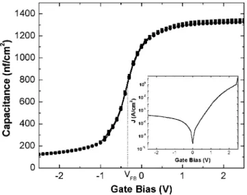
Figure 5 shows the 10 kHz and 100 kHz C–V character-istics and the J – V charactercharacter-istics of the sample spike an-nealed and anan-nealed in forming gas for 20 min. From the 100 kHz C–V curve, the EOT is 22.7 Å, with the quantum cor-rection, corresponding to k59.3. This is lower than that of ZrO2 due to the interfacial silicate layer. In addition, there is
slight frequency dispersion in the C–V curves, mainly below midgap. The inset to Fig. 5 shows the asymmetric J–V curve measured with light illumination for the same sample. The leakage current densities are 631024 A/cm2 at 1 V and
4.731026A/cm2at 21 V. For a pure SiO
2film with an EOT
22.7 Å, the leakage current density is about two orders of magnitude larger for a gate potential VG5VFB11 V.3
How-ever, the leakage is larger than expected from tunneling, Frenkel–Poole conduction, or Schottky emission.15 This
might be due to the difference of the barrier heights under different voltage polarity or might be due to a peaked distri-bution of traps in the dielectric that favors trap-assisted tun-neling for substrate injection.16 Further investigation of the
leakage mechanism is necessary but reducing the film sur-face roughness observed by HRTEM and AFM should im-prove performance.
IV. CONCLUSIONS
In this work it has been shown that thin stoichiometric, carbon-free ZrO2films can be deposited on Si~100! using the novel precursor Zr(Oi– Pr)
2(thd)2 dissolved in octane. O2
introduced into the chamber is necessary to reduce the car-bon contamination. XPS and HRTEM analysis shows that a Zr silicate layer is formed at the interface during deposition. Although the silicate layer reduces the effective dielectric constant of the gate dielectric, it may provide a better and more stable interface with Si.
The thin ZrO2 films exhibit good C–V and J–V
charac-teristics. After proper annealing treatments, an equivalent ox-ide thickness of around 2.3 nm has been achieved for a 5.2 nm thick film, with a leakage current two orders of magni-tude lower than that of SiO2 with the same EOT. The Pb
centers in the ZrO2 films were effectively passivated by FGA. The slight remnant frequency dispersion below midgap might be reduced if a proper FGA were performed after, rather than before gate electrode definition. These electrical properties demonstrate that thin ZrO2 films formed by
Zr(Oi– Pr)
2(thd)2 and O2 might be a promising gate
dielec-tric material for deep submicron CMOS devices if the rough-ness of the layers and the thickrough-ness of the interfacial layer can be reduced. In addition, it might be plausible to apply the thin ZrO2 films in flash memory as the gate dielectric over
the floating gate to increase the coupling ratio. However, further investigation of its reliability is indispensable before using this ZrO2 film process in CMOS technology.
ACKNOWLEDGMENTS
The authors are grateful to E. Estwick and T. Quance for the assistance in the preparation of the samples. The authors also wish to thank J. R. Hauser for use of the NCSU C–V analysis program. This work was supported by the National Science Council of the Republic of China under Contract No. NSC89-2215-E-009-071.
1The International Technology Roadmap for Semiconductors
~Semicon-ductor Industry Association, 2000!.
2S.-H. Lo, D. A. Buchanan, Y. Taur, and W. Wang, IEEE Electron Device
Lett. 18, 209 ~1997!.
3B. Brar, G. D. Wilk, and A. C. Seabaugh, Appl. Phys. Lett. 69, 2728
~1996!.
4D. J. Hubbard and D. G. Schlom, J. Mater. Res. 11, 2757 ~1996!. 5G. D. Wilk, R. M. Wallace, and J. M. Anthony, J. Appl. Phys. 89, 5243
~2001!.
6J. Robertson, J. Vac. Sci. Technol. B 18, 1785 ~2000!.
7W.-J. Qi et al., Tech. Dig. - Int. Electron Devices Meet., 145 ~1999!. 8W.-J. Qi et al., Tech. Dig. VLSI Symp., 40 ~2000!.
9C.-H. Lee et al., Tech. Dig. - Int. Electron Devices Meet., 27 ~2000!. 10A. C. Jones et al., Chem. Vap. Deposition 4, 46 ~1998!.
11J. R. Hauser and K. Ahmed, Characterization and Metrology for ULSI
Technology: 1998 International Conference,edited by D. G. Seiler, A. C. Diebold, W. M. Bullis, T. J. Shaffner, R. McDonald, and E. I. Walters ~The American Institute of Physics, Melville, N.Y., 1998!.
12S. Iwata and A. Akitoshi, J. Appl. Phys. 79, 6658 ~1996!. 13P. Lundgren and M. O. Andersson, J. Appl. Phys. 74, 4780 ~1993!. 14E. H. Nicollian and J. R. Brews, MOS (Metal Oxide Semiconductor)
Physics and Technology ~Wiley, New York, 1982!, p. 465.
15S. M. Sze, Phsyics of Semiconductor Devices, 2nd ed. ~Wiley, New York,
1981!, p. 403.
16M. Houssa, M. Tuominen, M. Naili, V. Afanas’ev, A. Stesmans, S.
Haukka, and M. M. Heyns, J. Appl. Phys. 87, 8615 ~2000!. FIG. 5. Frequency dependence of the C–V characteristics of a ZrO2film on
n1Si with an EOT of 2.27 nm after spike anneal at 850 °C in O
2for 1s and FGA at 380 °C for 20 min: ~jjj! 10 kHz, ~ddd! 100 kHz. A slight frequency dispersion is evident below midgap. The hysteresis ~DVFB;6 mV! is small. The inset shows the corresponding J–V curve, which is asym-metric and has a leakage current density of 631024A/cm2at 1 V ~substrate injection!.
1148 Chenet al.: Characterization of thin ZrO2films 1148