Publisher’s version / Version de l'éditeur:
Applied Physics Letters, 97, 153306, pp. 1-3, 2010-10-14
READ THESE TERMS AND CONDITIONS CAREFULLY BEFORE USING THIS WEBSITE. https://nrc-publications.canada.ca/eng/copyright
Vous avez des questions? Nous pouvons vous aider. Pour communiquer directement avec un auteur, consultez la première page de la revue dans laquelle son article a été publié afin de trouver ses coordonnées. Si vous n’arrivez pas à les repérer, communiquez avec nous à PublicationsArchive-ArchivesPublications@nrc-cnrc.gc.ca.
Questions? Contact the NRC Publications Archive team at
PublicationsArchive-ArchivesPublications@nrc-cnrc.gc.ca. If you wish to email the authors directly, please see the first page of the publication for their contact information.
NRC Publications Archive
Archives des publications du CNRC
This publication could be one of several versions: author’s original, accepted manuscript or the publisher’s version. / La version de cette publication peut être l’une des suivantes : la version prépublication de l’auteur, la version acceptée du manuscrit ou la version de l’éditeur.
For the publisher’s version, please access the DOI link below./ Pour consulter la version de l’éditeur, utilisez le lien DOI ci-dessous.
https://doi.org/10.1063/1.3499368
Access and use of this website and the material on it are subject to the Terms and Conditions set forth at
Impact of interfacial dipole on carrier transport in bulk heterojunction
poly„3-hexylthiophene and †6,6‡-phenyl C61-butyric acid methyl ester
blends
Tsang, S. W.; Drolet, N.; Tse, S. C.; Tao, Y.; Lu, Z. H.
https://publications-cnrc.canada.ca/fra/droits
L’accès à ce site Web et l’utilisation de son contenu sont assujettis aux conditions présentées dans le site LISEZ CES CONDITIONS ATTENTIVEMENT AVANT D’UTILISER CE SITE WEB.
NRC Publications Record / Notice d'Archives des publications de CNRC:
https://nrc-publications.canada.ca/eng/view/object/?id=edb33a61-09e9-4468-b234-a3253205f3a0 https://publications-cnrc.canada.ca/fra/voir/objet/?id=edb33a61-09e9-4468-b234-a3253205f3a0Impact of interfacial dipole on carrier transport in bulk heterojunction
poly„3-hexylthiophene… and †6,6‡-phenyl C
61-butyric acid methyl ester blends
S. W. Tsang,1,2,a兲 N. Drolet,2S. C. Tse,2Y. Tao,2and Z. H. Lu1,b兲1
Department of Material Science and Engineering, University of Toronto, Toronto, Ontario M5S 3E4, Canada
2
Institute for Microstructural Sciences, National Research Council of Canada, Ottawa, Ontario K1A 0R6, Canada
共Received 21 August 2010; accepted 20 September 2010; published online 14 October 2010兲 The electron transport properties in various poly共3-hexylthiophene兲 共P3HT兲 and 关6,6兴-phenyl C61-butyric acid methyl ester共PC61BM兲 blend films, prepared by various process conditions, were
investigated by admittance spectroscopy at different temperatures. It was found that the electron mobility and the dispersive transport behavior showed a strong dependence on the thermal treatment condition; the blend with the fastest growth rate had orders of magnitude reduction in the mobility and a much more dispersive transport. Using the Gaussian disorder model, it was found that the energetic disorder of the density-of-states between blends plays a significant role in the observed phenomena. It is proposed that the difference in the energetic disorder is due to the interfacial dipole effect at the P3HT/ PC61BM heterojunctions in the various blend films. © 2010 American Institute
of Physics.关doi:10.1063/1.3499368兴
It is well-known that the efficiency of the bulk-heterojunction organic photovoltaics cells 共OPVs兲 is highly sensitive to the nanoscale morphology of the active layer.1–5 It is mainly determined by the growth rate of the active layer right after spin-casting. The electron donor poly共3-hexylthiophene兲 共P3HT兲 and the electron acceptor 关6,6兴-phenyl C61-butyric acid methyl ester 共PC61BM兲 are
proto-typical materials in OPV technology. It has been demonstrated that the power conversion efficiency共PCE兲 for P3HT: PC61BM device can be varied from 3–6% with
differ-ent growth conditions of the polymer blend. Such variations in device performance is closely related to the balance be-tween the exciton diffusion and the carrier transport with different domain sizes of the donor and acceptor materials. It is generally believed that the degree of ordering of the active material, the spatial effect, is necessarily the key factor in determining the charge-carrier transport properties.6 How-ever, recently, it has been observed that a spontaneous trans-fer of a negative charge from P3HT: PC60in bilayer structure
forms an interface dipole.7 Similarly, in P3HT: PC61BM
bulk-heterojunctions, there are numerous interfaces between the individual materials. It can be deduced that the presence of the possible dipoles at these numerous interfaces will alter the charge-carrier transport properties in the blend film.
In this letter, the authors report on the electron transport properties in various P3HT: PC61BM blends as a function of
the film microstructure. Admittance spectroscopy 共AS兲, a powerful tool for probing the charge carrier dynamics, is employed to extract the electron mobility at various tempera-tures and to understand the physical mechanism for electron transport in the bulk-heterojunction thin films.
The samples fabricated in this study consist of a single active layer of P3HT: PC61BM 共1:1, wt %兲 sandwiched
be-tween an anode共Al, 70 nm兲 and a cathode 共Mg:Ag, 10:1, 50
nm兲 on glass substrates. The cathode was further covered by 50 nm of Ag used as capping layer. The metal electrodes were thermally evaporated in vacuum at a base pressure of 10−7 Torr. The active layers were prepared by spin-coating
the blend solution in dichlorobenzene onto the Al electrode. The organization in the active layer was controlled by vary-ing the growth rate of the active layer. Control of the growth rate was achieved by controlling the solution concentration, spinning speed and thermal treatment of the active layer after spin-coating. Details of the active layer preparation condi-tions are summarized in TableI. The growth rate in the dif-ferent samples was in the order of sample A ⬎ B ⬎ C ⬎ D. The thicknesses of the active layer were measured by a pro-filometer. The electron mobility in P3HT: PC61BM thin films
was characterized by AS with an HP 4284A LRC meter. Details of the principle and the experiment setup of AS have been reported elsewhere.8 Although electron injection from Mg:Ag into P3HT is possible, the injected electrons will be rapidly transferred to the PC61BM molecules which has a
lower lowest-unoccupied molecular orbital energy level. Prior to the charge carrier mobility measurements, any ab-sorbed ambient effect during sample transfer or residual sol-vent was eliminated by moderately heating the sample at 50 ° C for 24 h inside a temperature regulated cryostat with a base pressure of 10−6 Torr.
Figure1shows the typical capacitance versus frequency characteristics of the different samples measured by AS. A
a兲
Author whom correspondence should be addressed. Electronic mail: sai-wing.tsang@nrc-cnrc.gc.ca.
b兲Electronic mail: zhenghong.lu@utoronto.ca.
TABLE I. Summary of preparation condition of the P3HT: PC61BM 共1:1, wt %兲 blends. Sample Solution concentration 共mg/ml兲 Spinning condition 共rpm兲 Thermal treatment Thickness 共m兲 A 112 1000共60s兲 Baked 200 ° C 共30mins兲 1.20 B 112 1000共60s兲 Baked 100 ° C 共30mins兲 1.16 C 112 1000共60s兲 Naturally dried for 24 h 1.16 D 42.5 300共60s兲 Naturally dried for 24 h 1.50 APPLIED PHYSICS LETTERS 97, 153306共2010兲
0003-6951/2010/97共15兲/153306/3/$30.00 97, 153306-1 © 2010 American Institute of Physics
minimum capacitance Cminat a certain frequency is found in
samples B, C, and D. This feature corresponds to the space charge effect in the bulk of the material.8,9It also proves that a quasi-Ohmic contact is formed at the Mg: Ag/ PC61BM
interface.10 The electron mobilityecan be effectively
ex-tracted from the measured capacitance. Briefly, if Cminoccurs
at higher frequency it indicates a higher charge carrier mo-bility. Therefore, eincreases from sample B to sample D,
corresponding to a fast and a slow growth rate, respectively. Moreover, the degree of charge carrier mobility dispersion can be revealed by considering the ratio of Cmin/Cgeo, where
Cgeois the geometrical capacitance of the sample. In the case
of nondispersive transport, Cmin/Cgeo= 0.75.
8,9
The value of Cmin/Cgeoincreases for more dispersive transport. For highly
dispersive transport the capacitance minimum vanishes. As shown in Fig.1, there is no capacitance minimum observed in sample A. The value of Cmin/Cgeodecreases from 0.98 in
sample B to 0.92 in sample D, which suggests that the elec-tron transport becomes less dispersive as the growth rate of the active layer decreases. It is worth considering that the dispersive transport behavior can originate from the presence of trap states, or from the disordered properties of the trans-porting sites, both positional and energetic. However, since the samples are prepared with the same batch of materials, the variation in bulk trap states in different samples is safely excluded. Furthermore, it has been demonstrated that a slower growth rate of the active layer leads to a more ordered P3HT: PC61BM film.
3,5
Therefore, the difference of the dis-ordered properties between samples is attributed to the varia-tion in the observed electron transport behavior.
The electron mobilities of sample B, C, and D measured by AS at various temperatures are shown in Fig. 2. In gen-eral, the mobilities follow the Poole–Frenkel type of electric field F dependencee⬀ exp共F1/2兲, where is the field
de-pendence coefficient. It is found that ein sample B, which
has the fastest growth rate among samples B, C, and D, has the highest temperature and electric field dependence. From the measured e, the disordered properties of the electron
transporting site in PC61BM can be revealed by analyzing the
data with the Gaussian disordered model 共GDM兲:11
共E,T兲 = infexp
冋
−冉
2 3kT冊
2册
exp再
C冋
冉
kT冊
2 − ⌺2册
冑
F冎
, 共1兲whereinfis a prefactor, is the energetic disorder
param-eter that can be understood as the width of the Gaussian density-of-state 共DOS兲, ⌺ is the positional disorder param-eter, and C is a constant. By extrapolating the measuredeto
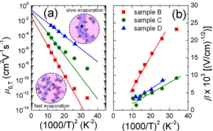
zero field, can be obtained from the plot of the zero field mobility0,Tversus 1 / T2as shown in Fig.3共a兲. On the other
hand, ⌺ can be extracted by plottingversus 1 / T2as shown in Fig. 3共b兲. The extracted disorder parameters for different samples are summarized in TableII. As expected, the largest positional disorder parameter ⌺ is found in sample B and the smallest in sample D. A more organized film of P3HT: PC61BM blend can be formed from a slower growth
rate of the active layer. Although it is generally believed that such improved ordering is only a result of the increase in crystalline packing of P3HT, there is no doubt that more PC61BM will also pack together to retain a constant effective
volume. This has been proved by the observed phase segre-gation between P3HT and PC61BM measured by atomic
force microscopy.4Surprisingly, there is a large difference in
TABLE II. Extracted GDM parameters of different samples from the mea-sured electron mobilityein Fig.3.
Sample inf 共cm2V−1s−1兲 共meV兲 C 共V / cm兲−1 ⌺ B 0.041 124 4.53⫻ 10−4 2.63 C 0.19 106 2.12⫻ 10−4 2.06 D 0.30 82 3.93⫻ 10−4 1.58
FIG. 1.共Color online兲 Measured capacitance vs frequency characteristics of sample A 共black, square兲 at T = 263 K and F = 2.0⫻ 105 V / cm; B共red, circle兲 at T = 263 K and F = 2.0⫻ 105 V / cm; C 共green, up-triangle兲 at T= 263 K and F = 2.0⫻ 105 V / cm; D共blue, down-triangle兲 at T = 270 K and F = 1.3⫻ 104 V / cm. The capacitance C is normalized to the geometrical capacitance Cgeoof individual sample.
FIG. 2. 共Color online兲 Measured electron mobilityevs square root of applied electric field F1/2of sample共a兲 B 共red兲, 共b兲 C 共green兲, and 共c兲 D 共blue兲. The solid lines are the best fit of the data to the Pool–Frenkel type of electric field F dependencee⬀ exp共F1/2兲.
FIG. 3. 共Color online兲 共a兲 The zero-field mobility0,Textrapolated from the measuredein Fig.2vs 1 / T2of sample B共red兲, C 共green兲, and D 共blue兲. 共b兲 The corresponding field dependence coefficient vs 1 / T2. The solid lines are the best fits to the data at temperature T ⬎ 220 K. Insets show the illustrations of the phase segregation of P3HT: PC61BM for slow and fast growth rate of the active layer. Interface dipoles are formed at P3HT: PC61BM heterojunctions.
153306-2 Tsang et al. Appl. Phys. Lett. 97, 153306 共2010兲
the energetic disorder parameter between different samples. As depicted in Eq. 共1兲, the low field mobility is mainly determined by theinfand. Taking sample B and D
as an example, infin sample B is about one order of
mag-nitude lower than that in sample D. However, a large value ofin sample B attributes to more than two orders of mag-nitude reduction in mobility. Extensive experimental studies on carrier transport properties in polymers doped with hole-transporting molecules have been reported by Borsenberger and co-workers,12,13with detailed discussion ofinfandin
different polymer hosts. The prefactor inf depends on the
intersite distance R and wave function decay constant␣, i.e.,
inf⬀ R2exp共−2␣R兲. Owning to the energy difference of the
transporting sites in P3HT and PC61BM, the wave function
overlap is larger between PC61BM molecules. Moreover, in a
less organized blend that with smaller degree of phase seg-regation, more PC61BM molecules are homogeneously
dis-persed with the P3HT polymers which increases the intermo-lecular distance R between the PC61BM molecules for
electron transport. Considering a typical value of ␣= 5 ⫻ 107
cm−1 for organic materials,14,15 and R varies from a few to tens of nanometers which depends on the processing conditions. A larger R in the less organized blend reduces the
inf. Despite the spatial effect, it is found that the increased
energetic disorder of PC61BM in the less organized blend
also plays an important role for the reduction in the electron mobility.
The variation in in different blend films can be ex-plained by considering the presence of interface dipoles be-tween P3HT and PC61BM. The dipolar effect on the energy
profile of the DOS and the charge-carrier transport in a dis-ordered media was originally proposed by Dieckmann16and Young17 under the framework of the GDM. The energetic disorder parameter takes into account both the dipole-induced disorder d and the Van der Waals interactions
be-tween moleculesvdw, i.e.,2=d 2
+vdw 2
. The additional d
broadens the Gaussian DOS which depends on the amount and the orientation of the dipole moments in the system.17It has been recently reported that there exists an interface di-pole between P3HT and C60 by photoemission study.
7
As-suming the magnitude of the dipole at the P3HT/ PC61BM
interface in different blend films are comparable, it is pro-posed that the origin of the difference ofdbetween samples
with slower and faster growth rate of the active layer is due to the variation of the interfacial area of the heterojunctions as illustrated in the insets of Fig. 3共a兲. Less phase segrega-tion between P3HT and PC61BM is expected for the film
grown faster. The area of the P3HT/ PC61BM interface, and
therefore the number of interface dipoles is larger inside this blend. Moreover, as the PC61BM phase is smaller, the
in-jected electrons have higher probability to experience the interface dipole effect during the multidirectional hopping process. This attributes to a larger overall energetic disorder
for the sample having a faster growth rate of the active layer. A largerreduces the electron mobility and results in much more dispersive transport behavior. In other words, in the absence of dipoles at the P3HT/ PC61BM interface, the
difference in charge carrier mobility between samples are
mainly determined by the prefactor inf and the positional
disorder parameter ⌺, which depends on the degree of the self-organization of samples. However, the presence of di-poles at the P3HT/ PC61BM interface additionally increases
the energetic disorder parameterwhich further reduces the charge carrier mobility. The contribution of the dipole disor-derdalso depends on the degree of the self-organization of
the samples; a largerdis expected in less organized blends
that have larger P3HT/ PC61BM interface area.
In conclusion, the electron transport properties in P3HT: PC61BM共1:1兲 blend films have been studied by AS at
various temperatures. It is found that both the electron mo-bility and the dispersive transport behavior depend strongly on the growth rate of the active layer. According to the re-sults of the measured electron mobility of different samples at various temperatures, the electron mobility is mainly de-termined by the variation in the energetic disorder, rather than by the spatial distribution of the transporting sites in PC61BM. This is proposed to be a result of the variation in
the induced-dipole disorder at the P3HT/ PC61BM interfaces
within the blend films. A faster growth rate with less phase segregation between P3HT and PC61BM leads to larger
ef-fective area of interfacial dipole at the P3HT/ PC61BM
het-erojunctions which impede electron transport in the blend films by increasing the energetic disorder of the DOS.
Financial support for this project was provided by Natu-ral Sciences and Engineering Research Council of Canada 共NSERC兲 and National Research Council Canada 共NRC兲.
1
W. Ma, C. Yang, X. Gong, K. H. Lee, and A. J. Heeger,Adv. Funct. Mater. 15, 1617共2005兲.
2
G. Li, V. Shrotriya, J. Huang, Y. Yao, T. Moriarty, K. Emery, and Y. Yang,
Nature Mater. 4, 864共2005兲. 3
Y. Kim, S. Cook, S. M. Tuladhar, S. A. Choulis, J. Nelson, J. R. Durrant, D. D. C. Bradley, M. Giles, I. McCulloch, C.-S. Ha, and M. Ree,Nature Mater. 5, 197共2006兲.
4
V. Shrotriya, Y. Yao, G. Li, and Y. Yang,Appl. Phys. Lett. 89, 063505
共2006兲. 5
C.-W. Chu, H. Yang, W.-J. Hou, J. Huang, G. Li, and Y. Yang,Appl. Phys. Lett. 92, 103306共2008兲.
6
R. Pacios, J. Nelson, D. D. C. Bradley, and C. J. Brabec,Appl. Phys. Lett. 83, 4764共2003兲; S. A. Choulis, J. Nelson, Y. Kim, D. Poplavskyy, T. Kreouzis, J. R. Durrant, and D. D. C. Bradley,Appl. Phys. Lett. 83, 3812
共2003兲; J. Huang, G. Li, and Y. Yang, Appl. Phys. Lett. 87, 112105
共2005兲. 7
W. Osikowicz, M. P. Jong, and W. R. Salaneck,Adv. Mater. 19, 4213
共2007兲. 8
S. W. Tsang, S. K. So, and J. B. Xu,J. Appl. Phys. 99, 013706共2006兲. 9
H. C. F. Martens, H. B. Brom, and P. W. M. Blom, Phys. Rev. B 60,
R8489共1999兲. 10
S. W. Tsang, S. C. Tse, K. L. Tong, and S. K. So,Org. Electron. 7, 474
共2006兲. 11
H. Bässler,Phys. Status Solidi B 175, 15共1993兲. 12
P. M. Borsenberger,J. Appl. Phys. 68, 5188共1990兲. 13
J. A. Sinicropi, J. R. Cowdery-Corvan, E. H. Magin, and P. M. Borsen-berger,Proc. SPIE 2850, 202共1996兲.
14
E. L. Wolf, Principle of Electron Tunneling Spectroscopy共Oxford Univer-sity Press, New York, 1995兲.
15
S. W. Tsang, M. W. Denhoff, Y. Tao, and Z. H. Lu,Phys. Rev. B 78,
081301共R兲 共2008兲. 16
A. Dieckmann, H. Bässler, and P. M. Borsenberger,J. Chem. Phys. 99,
8136共1993兲. 17
R. H. Young,Philos. Mag. B 72, 435共1995兲.
153306-3 Tsang et al. Appl. Phys. Lett. 97, 153306 共2010兲