HAL Id: hal-01068655
https://hal-univ-rennes1.archives-ouvertes.fr/hal-01068655
Submitted on 26 Sep 2014HAL is a multi-disciplinary open access
archive for the deposit and dissemination of sci-entific research documents, whether they are pub-lished or not. The documents may come from teaching and research institutions in France or abroad, or from public or private research centers.
L’archive ouverte pluridisciplinaire HAL, est destinée au dépôt et à la diffusion de documents scientifiques de niveau recherche, publiés ou non, émanant des établissements d’enseignement et de recherche français ou étrangers, des laboratoires publics ou privés.
Low-Return-Loss Printed Log-Periodic Dipole Antenna
Antoine Chauloux, Franck Colombel, Mohamed Himdi, Jean-Louis Lasserre,
Philippe Pouliguen
To cite this version:
Antoine Chauloux, Franck Colombel, Mohamed Himdi, Jean-Louis Lasserre, Philippe Pouliguen. Low-Return-Loss Printed Log-Periodic Dipole Antenna. IEEE Antennas and Wireless Prop-agation Letters, Institute of Electrical and Electronics Engineers, 2014, 13, pp.503 - 506. �10.1109/LAWP.2014.2310057�. �hal-01068655�
Low return loss Printed Log Periodic Dipole Antenna
Antoine Chauloux, Franck Colombel, Mohamed Himdi, Jean Louis Lasserre, and Philippe PouliguenAbstract - In this paper, a low return loss printed log periodic dipole antenna (PLPDA) fed by a coaxial cable is presented. The widths of dipole elements are optimized to increase the bandwidth. A study of coaxial cable position is included in order to improve the antenna behavior. The measured return loss is lower than -15 dB from 2.1 to 4.3 GHz. The measured gain varies between 6 dBi and 7 dBi. The measurements, including input impedance, gain and radiation patterns, and simulations are in agreement.
Index Terms - Printed log-periodic dipole antenna array (PLPDA), low return loss,
coaxial cable.
I. INTRODUCTION
OG-periodic dipole antennas (LPDA) are widely used because of their frequency independent radio electrical characteristics. This typeof antennas was recommended at the beginning of the 60’s [1]. In [2], R. Carrel demonstrates how to design a LPDA according to specifications in terms of bandwidth and directivity. For HF and VHF applications, there is no major practical limit for the use of such antennas. Nevertheless at microwave frequencies, it seems more convenient to use printed technology in order to make it as accurate as possible.
In [3], Campbell and al. demonstrate the design a two layer printed log-periodic dipole antenna (PLPDA) fed by a stripline conductor. The measured input impedance is in agreement with the simulation over 1 – 2 GHz range. Self-complementary structure can be employed for LPDA. Due to their constant impedance properties it allows very stable input impedance over a wide frequency range [4]-[5]. PLPDA could also be printed on both sides of the dielectric slab. In this configuration, every consecutive dipole element is printed on the opposite side of the substrate in order to have the required phase opposition for LPDA. Printed technology is very helpful to work on the antenna design for various optimizations such as size reduction [6]-[7] or gain improvement [8] or even bandwidth enhancement [9]. In [6] the simulated S11 is under -15 dB between 1.8 and 4.25 GHz whereas the measured
return loss rises and achieves -10 dB. In [7] the VSWR of a log-periodic Koch dipole antenna (LPKDA) is compared to the return loss of a Euclidean PLPDA. The measured VSWRs are lower than 2.35 (S11 = -8 dB) between 2.05 and 3.2 GHz for both antennas. PLPDA input
impedance is influenced not only by the antenna design but also the feeding system. One of the pl
A. Chauloux, F. Colombel and M. Himdi are with the Institut d’Electronique et
Télécommunications de Rennes (IETR) – Université de Rennes 1 – France. (e-mail : [email protected]; [email protected];
J.-L. Lasserre is with the CEA, DAM, GRAMAT, F-46500 Gramat, France (e-mail : [email protected])
P. Pouliguen is with the DGA/DS/MRIS (e-mail : philippe.pouliguen@ L
dga.defense.gouv.fr)
most common ways to feed a PLPDA is to use a coaxial cable as described by Carrel for free space LPDA [2]. On the one hand, the external shield of the cable is soldered to the boom printed on one side of the substrate. On the other hand, the inner conductor of the cable is connected to the opposite side of the boom directly through a hole drilled in the dielectric substrate. In this way the antenna acts as its own balun and wideband coverage can be achieved. Nevertheless, this technique modifies the antenna symmetry [10] and the return loss is usually around -10 dB in the whole frequency band. Two types of feeding techniques are presented in [8]. The first is a balanced feeding system with a coaxial cable soldered along one antenna’s side and the second is a differential feeding system. In this case a square patch is printed close to the smallest dipole element in order to solder a SMA connector that is used to connect a coaxial cable. The measured VSWR is maintained lower than 2 (S11 = -9.5 dB). When the balanced feeding system is used, the VSWR is worse.
In this paper, a PLPDA designed for High Power Microwave (HPM) applications is presented. The return loss of the antenna has to be very low (around -20 dB) in order to limit energy back to the power generator. It is placed over a ground plane and fed by a coaxial cable. The position of the cable and the scale factor of the antenna are optimized to improve the return loss level and the bandwidth. A set of measurements including S11, gain and
radiation patterns is presented and compared to simulation.
II. ANTENNA DESIGN
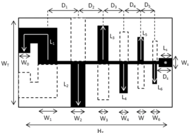
The proposed PLPDA is designed to operate between 2 and 4 GHz. As depicted in Fig. 1, the antenna is printed on a dielectric substrate and fed with a cable and placed over a ground plane (30 cm x 30 cm). The size of the ground plane is intentionally high because the presented PLPDA will be further included in an antenna array. The ground plane protects electrical devices associated with the antenna. Used coaxial cable is provided by Huber and Suhner (SM 141). Owing to its flexibility no additional mechanical support is needed to maintain the antenna in appropriate position. The cable is also low losses and its power handling is more than 200 W (CW) up to 4 GHz. The distance between the coaxial cable placed in parallel with the antenna’s boom is called d. The feeding point of the antenna was designed very cautiously – the outer conductor of the coaxial cable is soldered on one side of the antenna and the inner conductor of the coaxial cable runs through the substrate via a drilled hole and is soldered to the other side of the antenna. In order to solder the copper shield of the cable properly a small rectangular patch has been placed (LS = 6.8 mm, WS = 4.6 mm and DS = 7.8 mm) at the top of the antenna which means it is fed differentially. The other side of the cable is soldered to a copper ring which is screwed in the ground plane. A SMA connector is then soldered to the cable to feed the antenna under the ground plane. The antenna (see Fig. 2) is printed on a NELTEC dielectric substrate (NX9300) with εr = 3
and a thickness equal to 0.8 mm. According to [2], when scale and spacing factors are equal to 0.824 and 0.146 respectively, the expected gain is 8 dBi and the bandwidth is [2-4GHz] with 8 dipoles. In this case the total height of the antenna is 98 mm which exceeds our dimensional constraint. To lower this length to 85 mm, the smallest and the longest dipoles are removed. This leads to the decreasing of the frequency bandwidth of the antenna. In order to extend the upper part of the bandwidth, the lengths of the dipoles are adjusted. The length of the longest dipole is now 54 mm instead of 63 mm before modifications. Based on the length of the longest dipole, the lengths of other dipoles are calculated using the
procedure given in [2]. In order to reduce the width of the antenna, the longest dipole can be folded. The lengths and widths are Li and Wi respectively, L1 and W1 represent the
dimensions of the longest dipole. Distances between dipoles are Di (see Fig. 2.). The scale
factor is applied to determine the element’s sizes as follows: - L2= τ.L1 ; L3= τ.L2= τ².L1 ; …
- W2= τ.W1 ; W3= τ.W2= τ².W1 ; …
- D2= τ.D1 ; D3= τ.D2= τ².D1 ; …
The dipoles printed on back of the substrate are dotted in Fig. 2. We also point out that on the back of the printed circuit, the boom line continues up to the hole so there is no rectangular patch needed.
Fig. 1. PLPDA arranged above the ground plane - (a) Overview - (b) Front view - (c) Side view
Design details of the proposed antenna are shown in fig 2.
Fig. 2. Details of the design of the modified PLPDA on both sides of the substrate. Z X Y θ φ M A
III. RESULTS AND DISCUSSION
A. Antenna Optimization
The whole structure has been designed and simulated with the electromagnetic software CST Microwave Studio 2013. The design includes the PLPDA, the coaxial cable (designed following Huber and Suhner data sheet specifications) and the ground plane. The length of the coaxial cable under the ground plane is 5 cm and 12 cm on the antenna’s side of the ground plane. The first step of the optimization is focused on the S11 versus d, the distance between the cable and the substrate. In this first part, as mentioned in the previous section, L1 = 54 mm, τ = 0.824 and the spacing factor is equal to 0.146. Dimensions of the antenna
are those provided in Table 1.The S11 parameter is presented in Fig. 3 for 3 values of the
parameter d.
TABLE I
DIMENSIONS OF THE PROPOSEDPLPDA Half Dipole Length (mm) Dipole Spacing (mm) Element Width (mm) L1 27 D1 15.8 W0 5 L2 22.2 D2 13 W1 5 L3 18.3 D3 10.7 W2 4.1 L4 15.1 D4 8.8 W3 3.4 L5 12.4 D5 7.2 W4 2.8 L6 10.2 W5 W6 2.3 1.9
Fig. 3. Return losses of the proposed antenna versus d the distance between the antenna and the cable.
When d = 0, the coaxial cable is placed on the antenna’s boom in a balanced configuration [2]. There is an electrical contact between the outer conductor of the cable and the boom. In this first configuration, the return loss grows to -9.1 and -8.8 dB at 2.7 and 3.36 GHz. Simulations lead to a S11 close to -20 dB between 2.1 and 3.5 GHz when d is equal to 20
mm. This optimization demonstrates that by moving apart the cable from the antenna □ τ = τ τ = τ τ = τ □d = 0 mm d = 10 mm d = 20 mm
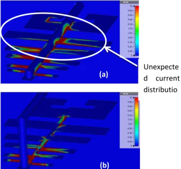
substrate, the return loss becomes lower. Fig. 4 highlights that, when d = 0, current among the outer conductor of the cable disrupts the current distribution of the antenna’s dipoles.
Fig. 4. Simulated current circulation on the PLPDA when d = 0 mm (a) and d = 20 mm (b) (F = 3.9 GHz).
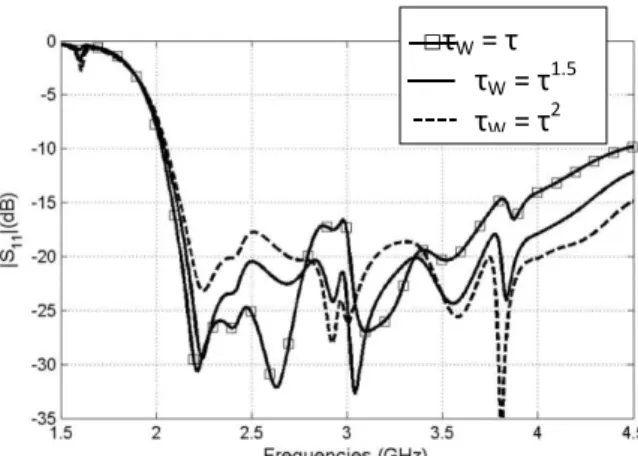
In a conventional design such as Carrel’s, the scale factor τ is the same for the width and the length of dipoles and the distance between dipoles. In the second step of optimization, we have calculated the S11 versus τW where τW is a scale factor used only for the width of the
dipoles. For the other parameters (length of dipoles and distance between them), scale factor τ is the same and equal to 0.824. In Fig. 5, we notice that the bandwidth and S11 level vary
versus τW. As a result when τW = τ1.5 = 0.75 the return loss is close to -20 dB in the frequency
range 2.16 – 3.9 GHz and lower than -15 dB up to 4.25 GHz. In table II, we have summarized the complete set of dimensions of the optimized PLPDA simulated with τW = τ1.5
and d = 20mm.
TABLE II
DIMENSIONS OF THE PROPOSEDPLPDA Dipole Length (mm) Dipole Spacing (mm) Element Width (mm) L1 27 D1 15.8 W0 6 L2 22.2 D2 13 W1 10 L3 18.3 D3 10.7 W2 7.5 L4 15.1 D4 8.8 W3 5.6 L5 12.4 D5 7.2 W4 4.18 L6 10.2 W5 W6 3.1 2.3 Unexpecte d current distributio n (a) (b)
Fig. 5. Return loss of the proposed antenna versus τW the scale factor applied for the width.
We highlight the fact that the total height (HT) and the width (WT) of the optimized antenna
are 79.5 mm and 46 mm respectively. The total height of the antenna is equal to 83.5 mm including the distance (4mm) between the ground plane and the top of the antenna.
B. Measurements and Simulations results
The optimized antenna has been manufactured and measured. Measurement of return loss is shown in Fig.6. The antenna was measured in an anechoic chamber in order to prevent parasitic reflection. So, the environment can be considered the same as in simulation. As depicted in Fig. 5, simulations and measurements are in agreement. The S11
is lower than -15 dB between 2.1 and 4.3 GHz. Moreover, we notice that the measured return loss is close to -20 dB in a large part of the frequency band. Despite the frequency bandwidth coverage being as wide as expected, the number of dipole elements is limited to 6 instead of 8 as recommended by Carrel [2].
Fig. 6. Return loss of the optimized PLPDA.
Measurement Simulation □τW= τ τW= τ 1.5 τW= τ 2
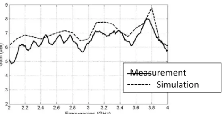
Fig. 7. Gain of the optimized PLPDA.
In Fig. 7, the simulated and measured gains are shown. The measured gain starts from 5 dBi at 2 GHz up to 8 dBi at 3.75 GHz. In the main part of the bandwidth, the gain varies between 6 and 7 dBi. The theoretical and the measurement resultsare in agreement.
(a) (b) (c) (d) (e) (f) Measurement Simulation Co-polar measurement Co-polar simulation Cross-polar measurement Cross-polar simulation
Fig. 8. Radiation patterns of the optimized PLPDA. (a) E plane for f = 2 GHz - (b) H plane for f = 2 GHz - (c) E plane for F = 3 GHz - (d) H plane for F = 3 GHz - (e) E plane for F = 4 GHz - (f) H plane for F = 4 GHz.
Fig. 8 depicts the radiation patterns for both E-plane and H-plane. To clarify, in the E-plane (Z0Y), E-θ and E-φ are the co-polarization and cross-polarization components respectively. In the H-plane (Z0X), E-φ is the co-polarization component whereas E-θ is the cross-polarization. The co-polarization simulations and measurements are in agreement for all frequencies. The -3dB beamwidth varies from 74° up to 86° and from 100° to 102° in the E-plane and H-E-plane respectively. The front to back ratio is better than 10 dB for the overall frequency band due to the antenna design and the size of the ground plane which is 30x30 cm. The cross polarization component measured in the H-plane of the antenna is higher than theone measured in the E-plane. However all values are lower than -10 dB compared to the co-polarization component for all frequencies.
IV. CONCLUSION
The design of printed log-periodic dipole antenna presented in this paper was obtained with two optimizations in order to allow a low return loss on a wide frequency range. It should be noted that the antenna is also size-reduced – in fact, the height of the antenna proposed in this paper is 83.5 mm instead of 98 mm foran antenna designed using Carrel procedure. The antenna is fed by a coaxial cable and the distance between this cable and the antenna has been optimized. An appropriate scale factor used for the width of dipoles has also been determined. As a result, the measured return loss is close to -20 dB between 2.2 and 3.9 GHz. The gain of this optimized antenna varies from 6 to 7 dBi. Theoretical results and measurements are satisfactory for all the significant parameters of the antenna. With the results described in this paper, we consider that this antenna should be a good candidate for high power applications.
V. ACKNOWLEDGMENT
This work was sponsored by the Commissariat à l’Energie Atomique et aux énergies alternatives (CEA) de Gramat and the Direction Générale de l’Armement (DGA). The authors are very grateful to Laurent Cronier and Christophe Guitton for the mechanical set up and would also like to extend their thanks to Jérome Sol and Laurent Lecoq for help with measurements.
REFERENCES
[1] D. Isbell, “Log periodic dipole arrays,” IRE Trans. Antennas Propag., vol. AP-8, no. 3, pp. 260-267, May 1960.
[2] R. Carrel, “The design of log-periodic dipole antennas,” in IRE Int. Convention Rec., 1961, pp. 61-75.
[3] C.K. Campbell, I. Traboulay, M.S. Suthers, H. Kneve, “Design of a stripline log-periodic dipole antenna,” Antennas and Propagation, IEEE Transactions on , vol.25, no.5, pp.718-721, Sep 1977
[4] Y. Mushiake, “Self-complementary antennas,” Antennas and Propagation Magazine,
IEEE , vol.34, no.6, pp.23,29, Dec. 1992
[5] Y. Mushiake, “A report on Japanese development of antennas: from the Yagi-Uda antenna to self-complementary antennas,” Antennas and Propagation Magazine, IEEE , vol.46, no.4, pp.47,60, Aug. 2004
[6] A. A. Gheethan and D. E. Anagnostou, “Reduced size planar log-periodic dipole arrays (LPDAs) using rectangular meander line elements,” in Proc. AntennasPropag. Soc. Int.
Symp., 2008, pp. 1-4.
[7] D. E. Anagnostou, J. Papapolymerou, M. M. Tentzeris, and C. G. Christodoulou, “A printed log-periodic Koch-dipole array (LPKDA),” IEEE Antennas Wireless Propag. Lett., vol. 7, pp. 456-460, 2008.
[8] S.M. Hashemi, V. Nayyeri, M. Soleimani, A.R.Mallahzadeh, “Designing a Compact-Optimized Planar Dipole Array Antenna,” Antennas and Wireless Propagation Letters,
IEEE , vol.10, no., pp.243-246, 2011
[9] A.A. Gheethan, D.E. Anagnostou, “The design of reconfigurable planar log-periodic dipole array (LPDA) using switching elements,” Antennas and Propagation Society
International Symposium, 2009. APSURSI '09. IEEE , vol., no., pp.1,4, 1-5 June 2009
[10] G.A. Casula, P. Maxia, G. Mazzarella, G. Montisci, “Design of a printed log-periodic dipole array for ultra-wideband applications,” Progress In Electromagnetics Research C, Vol. 38, 15-26, 2013.
[11] F.F. Dubrovka, M.M. Lytvyn, S.M. Lytvyn, S.Y. Martynyuk, Y.V. Ryabkin, O.O Vtorov, “Ultra wideband log-periodic dipole antenna arrays for the frequency range 0.7-12 GHz,” Antenna Theory and Techniques, 2005. 5th International Conference on , vol., no., pp.110,115, 24-27 May 2005
![[PPT] Formation CSS avec exemples d'application | Cours informatique](data:image/gif;base64,R0lGODlhAQABAIAAAP///wAAACH5BAEAAAAALAAAAAABAAEAAAICRAEAOw==)