Characterization and Analysis of Process
Variability in Deeply-Scaled MOSFETs
by
Karthik Balakrishnan
Submitted to the Department of Electrical Engineering and Computer
Science
in partial fulfillment of the requirements for the degree of
Doctor of Philosophy
at the
MASSACHUSETTS INSTITUTE OF TECHNOLOGY
ARCHIVES
MASSACHUSETS INSUiNE' OF TECHNOLOGYMAR 2
0
2012
LIBRARIES
February 2012
@
Massachusetts Institute of Technology 2012. All rights reserved.
Author ...
...
.
...
Department of Electrical Engineering and Computer Science
November 1, 2011
Certified by...
Professor of Electrical Engineering and
Duane S. Boning
Computer Science
Thesis Supervisor
,-.\ I i
Accepted by...
Leslie A. Kolodziej
ski
Chairman, Department Committee on Graduate Students
Characterization and Analysis of Process Variability in
Deeply-Scaled MOSFETs
by
Karthik Balakrishnan
Submitted to the Department of Electrical Engineering and Computer Science on November 1, 2011, in partial fulfillment of the
requirements for the degree of Doctor of Philosophy
Abstract
Variability characterization and analysis in advanced technologies are needed to en-sure robust performance as well as improved process capability. This thesis presents a framework for device variability characterization and analysis. Test structure and test circuit design, identification of significant effects in design of experiments, and decomposition approaches to quantify variation and its sources are explored. Two ex-amples of transistor variability characterization are discussed: contact plug resistance variation within the context of a transistor, and AC, or short time-scale, variation in transistors. Results show that, with careful test structure and circuit design and ample measurement data, interesting trends can be observed. Among these trends are (1) a distinct within-die spatial signature of contact plug resistance and (2) a picosecond-accuracy delay measurement on transistors which reveals the presence of excessive external parasitic gate resistance. Measurement results obtained from these test vehicles can aid in both the understanding of variations in the fabrication process and in efforts to model variations in transistor behavior.
Thesis Supervisor: Duane S. Boning
Acknowledgments
I would first like to thank my research advisor, Prof. Duane Boning. Duane, you have provided me with excellent research guidance and direction throughout this doctoral program. I have learned a tremendous amount from you about not just technical research, but also how to overcome difficult challenges and be in a position to be successful.
Three other professors provided excellent support and guidance over the last few years and their invaluable input helped me tremendously to complete this research. Prof. Dimitri Antoniadis helped to pinpoint the cause of systematic variations in the contact resistance measurement data and also gave numerous suggestions for strengthening the foundation of the AC variability work. Prof. Luca Daniel was helpful in placing my work in the larger framework of a characterization-modeling-mitigation context and provided suggestions for test structure design that yielded meaningful results. Prof. Vladimir Stojanovic's expertise in integrated circuit design aided me to better analyze the AC variability measurement results and determine their significance towards ICs. To all of them, I am extremely grateful for their time and patience in helping me complete this Ph.D research and thesis.
I would like to thank many of the research staff members at IBM Research. The summer internship opportunity extended to me by Dr. Keith Jenkins, Dr. Vijay Narayanan and Dr. Mukesh Khare turned into an ongoing collaboration which even-tually resulted in the AC variability characterization part of my thesis work. Keith and Vijay, you were both very helpful and I thank you for your support and guidance.
I also thank Dr. Leland Chang, Dr. Paul Solomon, and Dr. Jae-Joon Kim of IBM
Research for their technical support.
My family, of course, deserve my infinite gratitude for supporting me throughout. My mom, dad, and brother have all been very supportive of me and shown me lots
of love and I could not have accomplished this without them. To my fiance Lavanya - you have been extremely loving and caring from the time we met and I cannot thank you enough.
My friends have all been great to me and I have a huge amount of respect for
them. To my best friend Cyrus, I can't describe how good of a friend you are so I won't try. Michael, Daihyun, and Nigel - your friendship throughout the years has been invaluable and you have all helped me in so many different ways. Thanks to all of you for everything.
I am grateful to all the past and present members of the Boning research group, with whom I've shared many conversations about endless topics, and who have also helped me in numerous ways.
I acknowledge the support of the Interconnect Focus Center (IFC), one of five research centers funded under the Focus Center Research Program, a Semiconductor Research Corporation Program.
Contents
1 Introduction 25
1.1 Thesis Organization . . . . 31
2 Addressing Process Variation in Deeply-Scaled Technologies 33 2.1 Characterization of Process Variation in Devices . . . . 34
2.1.1 Classification of Transistor Parameters . . . . 35
2.1.2 Challenges in Variability Characterization . . . . 36
2.1.3 Test Structures for Device Variability Characterization . . . . 37
2.1.4 Statistical Metrology to Enable Variation Analysis . . . . 40
2.2 Modeling Device Variation . . . . 42
2.2.1 Variation-Aware Modeling for Devices . . . . 42
2.2.2 Variation Modeling for Unit Processes . . . . 44
2.3 Mitigating Process Variation . . . . 45
2.3.1 Mitigation at the Process Level . . . . 45
2.3.2 Mitigation at the Device Level . . . . 46
2.4 Sum m ary . . . . 47
3 Contact Plug Resistance Variability 3.1 Contacts in a Device Context . . . . 3.2 Background Work . . . . 3.2.1 Individual Contact Measurement
3.2.2 Failure and Defect Analysis . . . 3.2.3 Analytical Modeling . . . . 49 50 51 52 54 55
3.2.4 Arrayed Test Structures . . . .
3.3 Test Structure for Contact Plug Resistance Variability Characterization
3.3.1 Contact Plug Resistance Measurement Circuit . . . .
3.3.2 Simultaneous Contact and Device Measurement Circuit . . . . 3.3.3 Measurement Accuracy . . . .
3.3.4 Design of Experiments . . . . 3.4 Variation Decomposition Methodology . . . . 3.4.1 Spatial Correlation Computation . . . . 3.4.2 Decomposition of Variation Sources . . . . 3.4.3 Analysis of Variance (ANOVA) . . . . 3.5 Statistical Analysis Results . . . . 3.5.1 Overall Trends . . . .
3.5.2 Die-to-Die Trends . . . .
3.5.3 Within-Die Systematic Layout-Dependent Trends 3.5.4 Within-Die Systematic Position-Dependent Trends
3.5.5 Random Spatially Uncorrelated Variation . . . . . 3.5.6 Spatial Correlation Via Sparse Regression . . . . .
3.6 Simultaneous Bank Measurement Results . . . . 3.7 Need for Variability Models . . . .
3.8 Sum m ary . . . . 4 Array-Based Test Structure for AC Variability Characterization
4.1 Array-Based Test Circuit . . . . 4.1.1 DUT Array . . . .
4.1.2 Design Optimization for AC Variability Measurement . . . .
4.1.3 Signal Propagation . . . . 4.1.4 Delay Measurement Circuit . . . . 4.1.5 Measurement Setup and Methodology . . . . 4.1.6 Measurement Accuracy . . . . 4.1.7 Test Chip . . . . . . . . 60 . . . . 62 . . . . 62 . . . . 63 . . . . 65 . . . . 65 . . . . 66 . . . . 67 . . . . 69 . . . . 75 . . . . 77 . . . . 79 . . . . 80 . . . . 83 85 87 89 90 94 96 98 100 101 102
4.2 Summary ... .0
5 Ring Oscillator-Based Test Structure 105 5.1 Introduction . . . . 105
5.2 Transistor Propagation Delay . . . . 106
5.3 Test Circuit Description . . . . 108
5.4 Delay Measurement Circuit . . . . 111
5.5 Test Circuit for Compensation of SOI Variations . . . . 112
5.6 Simulation Results . . . . 112
5.6.1 RO-Based Test Circuit Accuracy and Sensitivity . . . . 114
5.6.2 Sensitivity of tmea, in the Absence of AC Variations . . . . 117
5.7 Test Chip . . . . 119
5.8 Measurement Results . . . . 120
5.8.1 Off-Chip Measurement Accuracy . . . . 122
5.8.2 Single-Die Results . . . . 122
5.8.3 Wafer-Averaged Results . . . . 124
5.8.4 Multiple Operating Voltage Results . . . . 125
5.8.5 Potential Circuit Impact and Implications . . . . 127
5.9 Summary . . . . 130 6 Conclusions 131 6.1 Contributions . . . . 131 6.2 Conclusions . . . . 133 6.3 Future Work . . . . 134 6.3.1 Characterization . . . . 135 6.3.2 Variation-Aware Modeling . . . . 135 6.3.3 Mitigation of Variation . . . . 136 102
List of Figures
1-1 Polysilicon CD window versus technology node in Intel's manufacturing
process [1]. Shrinking upper and lower bounds on allowable critical dimensions present a significant challenge to transistor scaling. . . . . 26
1-2 Random dopant fluctuation [2], causing the number of dopants and their locations in the within the channel of a transistor to vary from transistor to transistor. . . . . 27 1-3 Number of dopants decrease as a function of technology node, which
means that random dopant fluctuations in advanced technology nodes cause increased deviations relative to the mean [2]. . . . . 27
1-4 Constant standard deviation with scaling and linear relationship be-tween input parameter and output performance. An input parame-ter which has these characparame-teristics does not pose a variation or yield-related challenge to technology scaling. . . . . 28 1-5 Constant relative standard deviation with scaling and linear
relation-ship between input parameter and output performance. An input pa-rameter which has these characteristics does not pose a variation or yield-related challenge to technology scaling. . . . . 29 1-6 Constant standard deviation with scaling and superlinear relationship
between input parameter and output performance. An input parame-ter which has these characparame-teristics poses significant variation and yield-related challenges to technology scaling because the relative variation in output performance increases as the technology scales. . . . . 29
1-7 Constant relative standard deviation with scaling and superlinear
rela-tionship between input parameter and output performance. An input parameter which has these characteristics poses variation and yield-related challenges to technology scaling because the relative variation in output performance increases as the technology scales. . . . . 30
2-1 Multi-pronged approach for addressing process variation in deeply-scaled technologies: modeling, characterization and mitigation. ... 34
2-2 Simulations showing the effect of polysilicon pattern density variations on spatial RTA temperature distribution [3]. Before optimization to obtain uniform polysilicon pattern density across the chip area, the simulated RTA temperature is significantly higher for regions of low polysilicon pattern density than for regions of high polysilicon pattern density. After optimization, the temperature gradient across the chip
is reduced... 39
2-3 Transistor matching as it relates to device area [4]. The standard
de-viation of the difference in threshold voltage between two identically designed transistors is inversely proportional to the square root of the transistor area. Therefore, the scaling of transistors to smaller
dimen-sions increases the threshold voltage mismatch between them. .... 43
2-4 Example of how DFM is used in Intel's SRAM cell design from 90nm to 45nm nodes [3]. The implementation of single-orientation polysilicon, relaxed pitch features, and a polysilicon endcap process which results in square polysilicon ends can be seen as the SRAM cell scales from the 90nm node to the 45nm node. . . . . 46
3-1 Contact in the context of a transistor and relevant extrinsic parasitic resistances [5]. The parasitic resistance components which most signifi-cantly involve the contact are RCONTACT, RsILICIDE, and RINTERFACE.
However, other choices, such as that to use elevated source-drain re-gions, can significantly impact the magnitude of these parasitics and others. ... 51 3-2 Resistor-grid model of metal-semiconductor contact [6]. R' is the
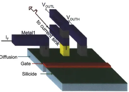
resis-tivity of the doped silicon source/drain junction and G' is the resisresis-tivity of the metal-semiconductor contact interface. . . . . 53 3-3 Three-dimensional transistor view with path of current flow through
contact to determine contact resistance of middle contact under test (yellow). The gate is switched off so no current flows from the source to the drain of the transistor itself. . . . . 57
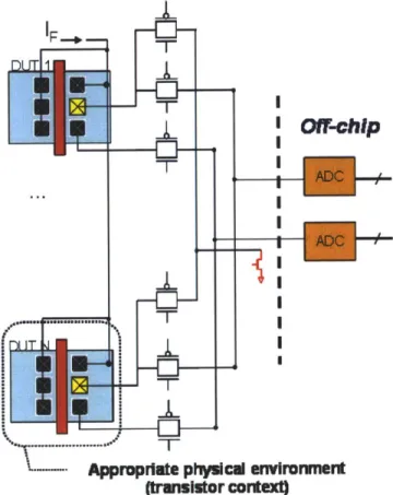
3-4 Test circuit to measure contact plug resistances in an arrayed set of DUTs. Three transmission gate switches are used to control access to
the VOUTL, VOUTH, and IF- Off chip-analog-to-digital converters are
used to sense the output voltages. . . . . 58 3-5 Test circuit to measure both contact plug resistances and transistor I-V
characteristics for an arrayed set of DUTs. An additional transmission gate switch is used to control the gate voltage of the transistor DUT and off-chip operational amplifiers are used to force the source and drain voltages to their desired values. The device current is measured through the measurement of voltage across an off-chip resistor that is
located in the current path of the DUT transistor. . . . . 59 3-6 Geometry-based variables in the DOE (half transistor shown for
sim-plicity). Contact-to-gate distance, (deg), contact-to-diffusion edge dis-tance (ded), and metallization layer to contact overlap for the y-dimension
(d,) are varied to determine any possible impact on contact plug
3-7 Design of experiments for contact resistance variability analysis. Values
are chosen such that many DUT geometries exist at or near "nominal"
case of dcg = 80nm, dcd = 40nm, and d, = 10nm. . . . . 61
3-8 Spatial correlation analysis-based variation decomposition
methodol-ogy. Spatially correlated contact plug resistance values can indicate the presence of a systematic trend, which can be subtracted from the measured data points to obtain a residual resistance map, for which the same analysis can be performed until there is no significant spatial correlation detected. . . . . 64
3-9 ANOVA results on wafer-level measurement data of contact plug
re-sistance. The largest sum of squares terms are those coming from the source-drain width parameter, the die parameter, and the error term for unexplained variance. The sum of squares of the three interaction terms are much smaller in comparison. . . . . 65 3-10 Contribution of each variation source to total variation in contact plug
resistance. More than half of the total variance can be attributed to die-to-die variations, while over 25% of the variance comes from the layout-dependent systematic component. Random within-die variation represents roughly 15% of the total variance. . . . . 66
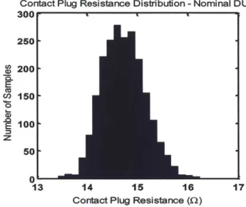
3-11 Distribution of measured contact plug resistances across one die. . . . 67
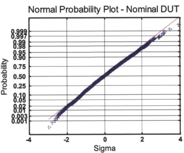
3-12 Normal probability plot of contact plug resistance measurements over
one die. . . . . 68 3-13 Distribution of measured contact plug resistances over the entire wafer,
which has a mean of 14.36Q and a standard deviation of 0.92Q. . . . 68
3-14 Normal probability plot of contact plug resistance measurements over the entire wafer show that the distribution is not Gaussian. In this case, this is due to the presence of various systematic effects due to various factors. . . . . 69
3-15 Wafer map of average die contact plug resistance for 43 measured die.
Given the observed data, no statistically significant wafer-level trend is observed. Some outlier die are located at the corners of the wafer. . 70 3-16 A plot of contact plug resistance resistance mean and standard
devia-tion versus dc shows an increase in mean contact plug resistance for those contacts which are located further away from the polysilicon gate of the transistor. However, the standard deviation of the measured re-sistance does not change as a function of dcg. . *.. . . . *71
-3-17 A plot of resistance mean and standard deviation versus dd shows an increase in mean contact plug resistance for those contacts which are located further away from the edge of the diffusion region of the transistor. However, the standard deviation of the measured resistance
does not change as a function of dd. . . . . 71
3-18 A 3D structure closely replicating the test structure design is used
for device simulations. Determining the current flow and electrostatic potentials at the surface of the silicide region can help to understand systematic trends in the measurement data. . . . . 72 3-19 A contour plot of electrostatic potential at silicon surface of a narrow
diffusion region shows that current crowding occurs near the top of contact B, resulting in some difference in average electrostatic potential between contacts B and C. . . . . 73 3-20 A contour plot of electrostatic potential at silicon surface of a wide
diffusion region shows that less current crowding occurs because of the large amount of diffusion area through which current can flow. In this case, the difference in average electrostatic potential between contacts B and C changes from its value in the case of a narrow diffusion region. 74
3-21 A plot of contact plug resistance as a function of source-drain width
shows that the average measured plug resistance increases with larger source-drain widths. For very large widths, the average resistance ap-proaches an asymptotic value. . . . . 75
3-22 Residual resistance as a function of column (x-location) shows two
dis-tinct regions of plug resistance. Contact plugs located at x > 1210pum have an average resistance which is 1.3% lower than those located at
x < 1210pm . . . . . 76
3-23 (a) Spatial correlation analysis computed with systematic die-to-die
effects included, (b) Spatial correlation analysis computed with sys-tematic die-to-die effects removed, (c) Spatial correlation analysis com-puted for single die located at wafer edge . . . . 78
3-24 Spatial maps of contact plug resistance for both a normal die and die located at edge are shown. The outlier die located at the edge of the wafer has an additional systematic spatial trend. . . . . 80 3-25 DCT coefficients from applying S-OMP-based algorithm on raw
mea-surement data reveal the periodic patterns present in the DUT array due to the repeating order of DUT types in the layout. . . . . 81 3-26 A die-level map showing systematic layout-dependent trends in contact
plug resistance, created from the extracted DCT coefficients from the measurement data, matches the distribution map of DUT types across the chip. . . . . 81 3-27 A scatter plot of normalized contact plug resistance versus normalized
transistor current, measured at V, = 1.OV and V, = 0.2V. A positive
correlation of 0.33 exists between the two variables. . . . . 82 3-28 Correlation coefficients between measured device currents at various
operating points and measured contact plug resistance. Correlations are strongest in the linear region of operation (low values of V, and
high values of Vd,). . . . . 83
3-29 A plot of device current as a function of Wed demonstrates that, while
ld is shown to be correlated with the contact plug resistance, the cause
is due to unintentional stress which is a function of the distance from the gate to the STI edge. . . . . 84
4-1 Some AC-relevant parasitics in a conventional MOSFET. The charac-teristics of such parameters are difficult to capture by performing DC measurements on the transistor, and therefore other characterization techniques which involve transients or high frequency operation are necessary. . . . . 88
4-2 A proposed test circuit design approach which measures delay variation among multiple transistors, but for which the delay is primarily due to targeted AC variation sources rather than all sources including DC sources such as threshold voltage and channel length. . . . . 89
4-3 Array-based test circuit schematic consisting of a clock source, an array of DUTs, and a delay detector. The relative delay mismatches through all DUTs in the array are measured by comparing the arrival time of node B, the DUT output, with the arrival time of node C, a common reference. . . . . 90
4-4 Schematic of a transmission gate DUT array. In this case, both the
DUT select enable device and the DUT are the same transmission gate. 91
4-5 Schematic of an NMOS DUT array. The input clock has access to the gate of one of the NMOS DUTs, controlled by the DUT select input and the transmission gates, and the output node is connected to a weak PMOS pull-up transistor to enable the output to swing high. . . . . . 91
4-6 Schematic of a PMOS DUT array. The input clock has access to the gate of one of the PMOS DUTs, controlled by the DUT select input and the transmission gates, and the output node is connected to a weak
NMOS pull-down transistor to enable the output to swing low. . . . . 92
4-7 Tradeoff involving number of DUTs in array versus AC variability cap-tured. A large number of DUTs results in a large load capacitance, which makes the overall transition at the drain dominated by DC vari-ation sources. On the other hand, a small load capacitance results in a DUT delay which is too small and whose variability can be over-whelmed by external variation sources. . . . . 93
4-8 DUT array optimization for AC variability characterization shows that
128 DUTs ensures that 98% of the variance in delay is attributable to AC variation sources. . . . . 95
4-9 Simulated DUT delay distributions for different array sizes and vari-ability sources. In the case of 8 DUTs, the distribution of delays when
AC variation sources are imposed differs significantly from that when
only DC variation sources are imposed. However, in the case of 1024 DUTs, the distributions are more similar to each other. . . . . 96
4-10 Variation in relative delay as a function of number of DUTs - DC
variations imposed versus all variations imposed. The point at which the distributions deviate from one another is qualitatively marked in
red... 97
4-11 A buffered H-tree for input signal propagation into transmission gate
array... .. .. . .. ... . .. . .. . . ... 98
4-12 Delay measurement technique using a logic gate followed by a first-order low-pass RC filter (NAND can be replaced with NOR depending
on whether the falling or rising edge needs to be characterized). . . . 99 4-13 Waveforms describing the operation of the delay measurement
tech-nique. Nodes B and C are the inputs to a NAND gate, whose output is shown in D. The low-pass filter then produces an average DC voltage,
VDC. --.-.--.-.-..-.-.-..-.-... .. 100
4-14 Limitations on accuracy of delay measurement technique. For up to 30ps of relative delay mismatch, the error in measurement is bounded
by 2ps. . . . . 101
4-15 The array-based test circuit layout is divided into three blocks: PMOS
DUT array, NMOS DUT array, and transmission gate DUT array. A
scan chain is implemented in the vertical direction which controls DUT access for all blocks. . . . 103
5-1 Propagation delay metrics which characterize the short time-scale
be-havior of a transistor. . . . . 107 5-2 Ring oscillator-based test circuit for AC variability characterization,
which operates in two modes and requires two clock period measure-ments and a delay measurement in order to characterize the DUT. . . 108 5-3 Waveforms at PMOS DUT terminals during pass mode, in which both
transitions at the drain of the DUT are triggered by transitions at the source of the DUT. . . . . 109
5-4 Waveforms at PMOS DUT terminals during wait mode, in which one transition at the drain of the DUT is triggered by a transition at the source of the DUT, while the other transition at the drain of the DUT is triggered by a transition at the gate of the DUT. . . . . 110 5-5 Array of RO blocks for statistical characterization of DUT AC
per-formance. Both the ring oscillator period and delay measurement pins are shared outputs, while each RO is accessed through an enable signal controlled by a scan chain. . . . . 110 5-6 Delay measurement using a logic gate and RC filter, which converts the
delay between two signals into a pulse whose duty cycle is proportional to the delay, and the converts the pulse into a DC voltage whose value is also proportional to the delay. . . . . 111 5-7 Modification of pass mode operation to minimize variations due to SOI
history effect difference between modes. The XOR gate before the pass switch only affects the pass mode of operation, while leaving the wait mode of operation unchanged. . . . . 113 5-8 Waveform at PMOS DUT terminals during pass mode in SOI history
effect-compensated test circuit. The average duty cycle of Vg, is similar in both the pass and wait modes of operation by creating periods during which time the DUT gate is switched off when it does not affect the propagation of the source signal to the drain. . . . . 113
5-9 Ring oscillator waveforms for NMOS DUT type show how the
transi-tions occur during the two modes of operation. . . . . 114
5-10 Ring oscillator waveforms for PMOS DUT type show how the
transi-tions occur during the two modes of operation. . . . . 116 5-11 Quantile-quantile plot showing tmeas distributions under DC variations
and all variations. The distribution of tmeas when the DUT is subject to all variation sources deviates from the case of only DC variation sources at a low standard deviation value. . . . . 116 5-12 Simulation results showing a plot of the distribution of tmeas when only
certain DC variation sources are present. These results indicate that threshold voltage is the parameter to which the output parameter tmeas is m ost sensitive. . . . . 118 5-13 A normal probability plot showing the simulated decomposition of
dif-ferent DC variation sources and how sensitive tmeas is to each of them. Threshold voltage variation is the DC source predominantly captured
by the output parameter, tmeas. . . . . 118
5-14 Ring oscillator layout showing the device under test (DUT), inverter stages, a logic block, and the resistor used for the delay measurement block. . . . 119
5-15 Test circuit layout which includes four ring oscillator blocks which
char-acterize NMOS DUTs and PMOS DUTs in both standard and SOI-compensated configurations. . . . . 120
5-16 Schematic of identifier RO block, which includes an external gate
re-sistor in series with the gate of the DUT. . . . 121
5-17 Layout of identifier RO block, which includes a 30kQ polysilicon
resis-tor connected to the gate of the DUT. . . . 121
5-18 Measured output parameters for PMOS DUTs on a single chip show
5-19 tmeas for PMOS DUTs on a single chip, calculated from the direct
measurement results in Figure 5-18. Identifier DUTs which exhibit larger values of tmea, are clearly distinguishable from other data points. 123
5-20 tmea, for all DUTs averaged over 40 die on wafer shows the presence
of identifier DUTs more clearly, in addition to some weak systematic trends due to power supply variations. . . . . 124
5-21 Schematic for PMOS DUT-based RO, showing all transistors and gates
as well as their relative sizes. . . . . 125 5-22 Schematic for NMOS DUT-based RO, showing all transistors and gates
as well as their relative sizes. . . . . 126 5-23 tmea, for multiple VDDL values for PMOS DUT shows that the identifier
is distinguishable at all voltages, but some voltage-dependent effects also change the measurement values relative to one another. . . . . . 128
5-24 tmea, for multiple VDDL values for NMOS DUT shows that the identifier
is distinguishable at all voltages, but some voltage-dependent effects also change the measurement values relative to one another. . . . . . 128 5-25 Simulation study of a 7-stage ring oscillator frequency variation due to
AC variation sources equal to that measured from the test chip, scaled
to a 32nm technology node. Results indicate that the frequency has a
List of Tables
2.1 Classification of device-related parameters to enable the understanding of challenges involved in device variability characterization. . . . . 35 3.1 Layout design parameter values chosen for the DOE: 4 factors and 55
DUT types representing a subset of all possible combinations of these
4 factors . . . . 62 5.1 Transistor and gate parameters for ring oscillator-based test circuit. . 127
Chapter 1
Introduction
In 1965, Gordon Moore observed that every 18 months, the density of transistors on a die increased by a factor of two [7]. This observation, which has been rebranded "Moore's Law" by the microelectronics industry consumers, has propelled the micro-electronics industry forward at an astonishing pace over the past 30 years. However, the challenges of integrating billions of transistors on a single die are becoming in-creasingly difficult to overcome. Fabricating two nominally identical transistors so that they behave identically is not possible due to imperfections and non-uniformities in the manufacturing process, also known as process variations. With smaller transis-tors and increased transistor density, the effect of process variations is more significant and meeting performance and yield specifications is increasingly challenging.
One example of process variations becoming more significant with scaling involves transistor gate length. Transistor gate length is a key parameter, along with gate pitch, that ultimately determines overall transistor density. For this reason, the min-imum feature size able to be fabricated for a given process technology, which is used to create a transistor gate, is also known as the gate "critical dimension" (CD). A technology node is defined as the minimum half-pitch between two features that is printable for that given technology. The technology node therefore serves as a mea-sure of achievable transistor density for a given technology. Shown in Figure 1-1 is the polysilicon CD target window for Intel at their different technology nodes to achieve yield and performance specifications for that node [1]. As the technology node
be-Poly Gate 3 Sigma window verse Technology nodes 500 400 300 -UCL Target 200 -- LCL 100 a. 0 0 50 100 150 200 250 300 350 400 Technology Nodes nm
Figure 1-1: Polysilicon CD window versus technology node in Intel's manufacturing process [1]. Shrinking upper and lower bounds on allowable critical dimensions present a significant challenge to transistor scaling.
comes more (smaller number), the window of allowable polysilicon CD, represented
by the red line upper and lower control limits, shrinks. For previous technology nodes
such as 0.35pum, process variations which cause the CD to differ across multiple tran-sistors is more tolerable because there is more margin for variations in CD. However, for advanced technology nodes such as 32nm and 22nm, the CD can only vary by a small amount, which is difficult to achieve in the presence of process variations. As an example, from Intel's 130nm to the 32nm technology node, both the scaling factor for the channel length and the bounds on the upper and lower control limits, have been the same (around 0.7) [8]. This indicates that the percentage tolerance limits on channel length as calculated from the nominal value are staying the same as technology scales.
Fabricating nominally identical transistors which behave identically has become more difficult due to scaling for other reasons as well. For example, the number of dopants in the transistor channel must be controlled to within certain boundaries to ensure performance and yield specifications are met. Figure 1-2 shows Intel's simulated distribution and location of dopants within the channel of a transistor [2]. Random dopant fluctuation (RDF) is a form of process variation resulting in variations in the number or location of dopant atoms implanted into the channel of each transistor. For previous technology nodes where the channel had a large area and
Figure 1-2: Random dopant fluctuation [2], causing the number of dopants and their locations in the within the channel of a transistor to vary from transistor to transistor.
the average number of dopants was large, the statistics of large numbers meant that the distribution of the number of dopants for multiple transistors was very tight with a small variance. In that case, RDF did not have a significant effect. However, when the transistor shrinks, the average number of dopants in the channel decreases, as shown in Figure 1-3 [2]. Consequently, there is less of an averaging effect when observing the number of dopants across multiple transistors. These increased deviations relative to the mean are larger, which in turn makes RDF more problematic. This is a difficult challenge because overcoming process variations in order to control the number or location of dopants in the transistor channel so precisely is difficult.
100000 a
E
10000ES
1000 100 10 1 10000 1000 100 10 1Technology Node (nm)
Figure 1-3: Number of dopants decrease as a function of technology node, which means that random dopant fluctuations in advanced technology nodes cause increased deviations relative to the mean [2].
With continued Moore's Law scaling, one can expect that process variations will play a more significant role in ultimately determining the performance and yield of a chip designed using a particular technology. To demonstrate this more clearly, it is useful to determine how both the absolute and relative variations of input parameters scale with technology, as well as the nature of the relationship between the input parameters and the performance and yield. First, the relative variation of a device parameter, represented by the quantity ", may scale with technology node in multiple ways. It may decrease, increase, or remain constant with technology scaling. Second, the relationship between the device parameter and the performance metric of interest may be linear, sublinear, or superlinear. Four examples are shown for hypothetical input parameters and relationships to the output performances in Figures 1-4, 1-5,
1-6, and 1-7.
Constant a scaling,
linear
I) - -CL ~~. ....144 . ... input Pnew Poldscaling
Figure 1-4: Constant standard deviation with scaling and linear relationship between input parameter and output performance. An input parameter which has these char-acteristics does not pose a variation or yield-related challenge to technology scaling.
Each device parameter which impacts performance, and whose variation impacts yield, can be categorized in this manner. For example, the scaling of channel length variation with technology can be characterized as having a constant relative standard deviation with respect to the mean channel length for a given technology. In
addi-Constant a/p scaling,
linear
0 input Pnew Pold4scaling
Figure 1-5: Constant relative standard deviation with scaling and linear relationship between input parameter and output performance. An input parameter which has these characteristics does not pose a variation or yield-related challenge to technology scaling.
Constant a scaling,
superlinear
0 input Pnew Poldscaling
Figure 1-6: Constant standard deviation with scaling and superlinear relationship between input parameter and output performance. An input parameter which has these characteristics poses significant variation and yield-related challenges to tech-nology scaling because the relative variation in output performance increases as the
Constant alp scaling,
superlinear
Cao
input
Pnew Pold 'scalingFigure 1-7: Constant relative standard deviation with scaling and superlinear re-lationship between input parameter and output performance. An input parameter which has these characteristics poses variation and yield-related challenges to tech-nology scaling because the relative variation in output performance increases as the technology scales.
tion, the relationship between channel length and performance, or more specifically saturation current in this case, can be described as superlinear. Because the device saturation current depends inversely on the channel length of the device, a percent deviation from a smaller nominal channel length will result in a larger percent de-viation in saturation current than that caused by the same percent dede-viation from a larger nominal channel length. Similarly, the number of dopants in the channel play a significant role in determining threshold voltage, and consequently, leakage current. The number of dopants scaled with technology in a constant standard devi-ation manner, but the reldevi-ationship between threshold voltage and leakage current is exponential in nature. Therefore, it can be concluded that random dopant fluctua-tion will cause more variafluctua-tion with technology scaling. Considering these effects along with variations in other device parameters, it is apparent that process variations will play a more significant role in determining yield and performance as the technology continues to scale.
being explored in order to continue Moore's Law scaling. These novel approaches are likely to be sensitive to process variations, both well-studied and new. With that serving as motivation, this thesis contributes test circuit-based methodologies to characterize such variations and statistical analysis tools to better understand them.
1.1
Thesis Organization
Challenges associated with addressing process variation are presented in Chapter 2. Previous work in the development of test structures to characterize transistor vari-ations is described and a classification of transistor parameters for the purposes of variation-related analysis is introduced. Two ways of coping with variation, namely modeling and mitigation, are discussed. On the modeling front, methodologies to in-corporate variation in existing component models as well as techniques for fast circuit simulation using such variation-aware models are described. Variation-based models for unit process steps in IC manufacturing are also discussed. On the mitigation front, existing techniques to reduce transistor variation in two different areas are presented: design for manufacturability (DFM) and process control.
Chapter 3 presents a test structure-based methodology for characterizing contact plug resistance. After motivating the need for such work, a test structure is presented along with a variation decomposition methodology. Then, silicon measurement results from a test chip are presented and various trends are described. The chapter concludes with a discussion on the need for variability-aware models for future technologies.
The need for the analysis of AC, or short time-scale, performance variations in transistors is motivated and an array-based test structure to characterize them is presented in Chapter 4. Such short time-scale variations in transient behaviors can be caused by variations in device geometries, parasitics, or other device parameters. A design-time optimization is used to make the test circuit sensitive to individual device
AC variations, and simulation results are shown which illustrate the effectiveness of
the measurement technique. Furthermore, the implementation and fabrication of a test chip are outlined along with details regarding the measurement setup and
methodology.
Then, Chapter 5 continues the discussion on AC variation analysis by introducing another test circuit to characterize the same. A ring oscillator-based test structure is introduced and simulations are shown which confirm the high sensitivity of the measurement technique to AC variation sources. Then, silicon measurement results from a test chip are presented and analyzed.
Finally, Chapter 6 concludes with a summary of this thesis and thoughts for future work in this area to address the challenges outlined earlier.
Chapter 2
Addressing Process Variation in
Deeply-Scaled Technologies
Addressing the impact of process variation in deeply-scaled technologies requires a multi-pronged approach involving variability characterization, variation-aware mod-eling, and techniques for mitigation. Such an approach is necessary whether the issues involving process variation are tackled at the process, device, circuit, or sys-tem level. This discussion will focus on the challenges of addressing variation in devices, although a fair bit of overlap will inevitably exist with the process and cir-cuit levels. A diagram of how such a multi-pronged approach might work is shown in Figure 2-1. The problem of addressing process variation in deeply-scaled transistors begins with variability characterization, which will be discussed in more detail in Sec-tion 2.1. The combinaSec-tion of test structure design and statistical metrology serves this function. Then, the results of the variability characterization and analysis can be fed into two different areas. One area is in variation modeling (Section 2.2). For device-level variation trends, the variations caused by different processing steps such as lithography, etch, oxide growth, ion implantation, annealing, and polishing can be modeled. In addition, the devices themselves lend themselves to variability-aware compact modeling, which works towards modeling variations in device performance due to variations in transistor parameters. Finally, the results of variability charac-terization of devices can also lead to techniques for mitigation. In the device and
Modeling Prcs anMitigation
charact riztion
Figure 2-1: Multi-pronged approach for addressing process variation in deeply-scaled technologies: modeling, characterization and mitigation.
circuit spectrum, design for manufacturability, or DFM, is based on improving circuit performance and yield by employing design techniques informed by variability data. In the IC manufacturing process, statistical process control is used to improve yield
by ensuring that steps in the manufacturing process will meet relevant specification
bounds. This control is guided by results of variability characterization of the process steps through the use of test structures. A detailed discussion on mitigating variation will be presented in Section 2.3.
2.1
Characterization of Process Variation in
De-vices
The characterization of process variation in deeply-scaled devices involves two ma-jor components: test structure design/measurement and variability decomposition. Before delving into the realm of existing research in these areas, it is useful to clas-sify transistor parameters into different groups to better understand the challenges of device variability characterization. The classification outlined in the following sec-tion also helps to understanding the compact modeling of variasec-tion in devices, as the characterization and modeling efforts are generally closely coupled.
2.1.1 Classification of Transistor Parameters
The characterization of a set of transistors and the determination of the distribution of one or more parameters requires an understanding of four mostly non-intersecting sets of transistor parameters: physical device parameters, device model parame-ters, device-measurable parameparame-ters, and geometry-based layout parameters. Some of these key parameters are shown in Table 2.1 and are discussed in more detail in Section 2.1.1.
Relevant Device-Related Parameters
Physical Device Device Model Device-Measurable Layout channel doping threshold voltage saturation current channel length dopant locations carrier mobility drain leakage current channel width
oxide thickness intrinsic gate cap. gate leakage current source/drain areas channel length source/drain resistance DIBL coefficient well proximity
channel width other parasitic RC sub-threshold swing distance to shapes cutoff frequency pattern density
unity gain frequency
Table 2.1: Classification of device-related parameters to enable the understanding of challenges involved in device variability characterization.
Physical device parameters are physical (non-electrical or structural) parameters whose values are the direct result of the process steps involved during transistor fabrication. Channel doping concentration, NA, locations of the dopant atoms, gate oxide thickness, t,., effective channel length, Leff, and channel width, W, are some fundamental transistor parameters which may differ from transistor to transistor due to variations in the manufacturing process.
Device model parameters are those which are derived from physical device param-eters and geometry-based layout paramparam-eters and used to model transistor behavior. Some of these parameters include threshold voltage, VT, electron or hole mobility,
p, intrinsic gate capacitance, COG, source-drain resistance, Rd, and various parasitic resistances and capacitances associated with the extrinsic portion of the transistor.
Device-measurable parameters are those which can be relatively easily charac-terized by low or high-frequency electrical voltage or current-based measurements of a device. Some of these parameters include drain saturation current, ID,sat,
off-state leakage current, Ioff, drain induced barrier lowering (DIBL) coefficient, r,
sub-threshold swing, S,_th, cutoff frequency, fT, and unity gain power frequency, fmax.
These measurements can usually be made using dedicated probe pads for each tran-sistor during in-line testing.
Geometry-based layout parameters are those which can be manipulated at the integrated circuit-design level. While, for a particular transistor type, a circuit de-signer cannot change the gate oxide thickness or channel doping for each individual transistor, geometry-based layout parameters may be changed. Some of these layout parameters may include the drawn channel length, Ldawn, the channel width, W,
the area of the source and drain regions, the number of contacts and their locations within the source and drain regions, the proximity of the transistor to a well, the separation distances to nearby polysilicon, active, and shallow trench isolation (STI) shapes, and effective pattern density.
2.1.2
Challenges in Variability Characterization
Two challenges in variability characterization and modeling stem from the previous discussion involving the classification of transistor parameters.
First, the relationship between device-measurable parameters and device model parameters is interdependent and correlated. As a result, building a test structure which determines the variances of a set of device-measurable parameters may not necessarily lead to the determination of the variances of a set of device model pa-rameters. Careful test structure design and circuit simulation are often required to
determine variances in model parameters with confidence.
Second, the relationship between the physical device structure parameters and the device model parameters is also interdependent and correlated by nature. There-fore, attributing a variation in a device-measurable parameter to variations in one or more physical device parameters requires a carefully planned design of experiments, adequate replication, and a sound variation decomposition methodology.
2.1.3
Test Structures for Device Variability Characterization
With the challenges in variability characterization now described, it is important to discuss test structures to characterize such device variability which have been developed over the years. While the characterization of individual transistors by using dedicated pads has its advantages in ease of design and measurement, statistical data necessary for variation analysis cannot be obtained without adequate replication. The variability characterization of deeply-scaled transistors can be performed in two ways. The first can be described as isolation-based characterization, in which an isolated parameter which has an impact on the overall transistor variation is characterized. Examples of such parameters are threshold voltage and channel length. The second is to obtain a more holistic or broad set of measurements on each of multiple transistors. This would include test structures that, for example, measure the I-V characteristics of multiple transistors in an array.Isolation-based Test Structures
One important parameter in devices as they have scaled has been the threshold voltage (VT). Because variability in device performance and leakage has increased substan-tially due to VT variation as technology has scaled, a number of test structures have been developed to characterize it. For example, [9] uses a test structure comprised of an array of devices whose individual off-state leakage currents are measured by an on-chip integrating analog-to-digital converter. Then, device equations are used to obtain relative intrinsic threshold voltage values for each device. Another approach, presented in [10], focuses on monitoring VGS for each transistor in an individually addressable array for a fixed current and then correlating that value back to the threshold voltage of the device.
Another important transistor parameter is its gate length, which can change across transistors due to variations in the lithography and etch processes. In order to deter-mine the critical dimension (CD) variability for a given technology, a test structure was designed in [11] which measured the CD of multiple polysilicon lines through
electrical resistance measurements.
Another variation-related issue, particularly for analog circuit and memory ap-plications, is matching between two or more identically designed devices. Therefore, a significant amount of work has been done to characterize the mismatch between transistors. For example, [12] discusses a test circuit that uses current mirrors to characterize transistor mismatch in the sub-threshold region of operation. More re-cently, a large addressable array of devices was characterized to assess the impact of different doses of implantation on the mismatch in both individual device threshold voltage and leakage current [13]. In this work, the leakage current of each device was measured while using techniques to cancel the off-state leakage of the other devices in the array which were not being measured.
More recently, studies have also been done to analyze the impact of other sources of variation. One such source is the rapid thermal annealing (RTA) process. Differ-ent pattern densities of polysilicon or shallow trench isolation (STI) may change the annealing temperature and therefore transistor properties. This is illustrated in simu-lation results performed by Intel, which shows that the annealing temperature during the RTA process varies across a die when dummy polysilicon is not used to create a uniform polysilicon density (Figure 2-2). However, a uniform pattern density makes the temperature profile across the die more uniform. To investigate the consequences of this effect, a test structure was designed to determine the impact of different pat-tern densities on doped poly-silicon sheet resistance, gate length, transistor currents,
and ring oscillator frequencies [14]. Each structure was carefully designed to maximize the impact of potential RTA-induced variations by modulating the pattern densities accordingly. In addition, the impact of shallow trench isolation (STI) edge effects on transistor variability was also characterized in [15]. In this work, a mismatch sweep analysis technique is used, in which intentionally dissimilar pairs of transistors are laid out and measurement results are used to quantify the impact of STI-induced stress variations.
While most of the previously discussed structures focus on front-end-of-line (FEOL) variations, a significant amount of research has also been done on investigating
back-0.800 -Poly Layout Extraction .. 00- Temperature --.a- ISimulation 4.00 --
-4.00-Figure 2-2: Simulations showing the effect of polysilicon pattern density variations on spatial RTA temperature distribution [3]. Before optimization to obtain uniform polysilicon pattern density across the chip area, the simulated RTA temperature is significantly higher for regions of low polysilicon pattern density than for regions of high polysilicon pattern density. After optimization, the temperature gradient across the chip is reduced.
end-of-line (BEOL) variations. One such example involves the building of a test structure to investigate variations in the chemical-mechanical polishing (CMP) pro-cess due to layout-based pattern-dependent effects such as feature area, density, and pitch [16].
Holistic-based Test Structures
A variety of test structures have been designed which obtain I-V characteristics of
multiple transistors located in an array or a bank. Often, one primary objective of such a test structure is to quickly gather data for a large number of devices so as to enable in-line characterization. Such is the case in [17] and [18], where a scribe line test structure is built for product wafer monitoring which obtains I-V character-istics for transistors quickly by using parallel testing methods and pad multiplexing. Similarly, an integrating ADC-based approach for obtaining I-V characteristics of multiple transistors was employed in [19]. In addition, an array of devices which
included transistors, capacitors, resistors, and ring oscillators, was designed in [20] as a comprehensive test vehicle for technology characterization. Leakage-minimization and noise immunity techniques were employed in order to obtain high-accuracy cur-rent and voltage measurement for the various test blocks.
2.1.4
Statistical Metrology to Enable Variation Analysis
Once measurement data is obtained from any test vehicle, one primary objective is to use the measurement results to obtain information about the potential variation sources at work, their relative magnitudes, and relationships among them. To perform such a task generally requires the use of statistical tools to determine the relationships between input design parameters, such as transistor size, surrounding layout geome-tries, or layout pattern density, and measured output parameters, such as threshold voltage, channel length, saturation current, gate capacitance, or transistor delay.In [21], the concept of statistical metrology as it applies to the semiconductor manufacturing process is introduced. Furthermore, the term "statistical metrology" is defined as "the body of methods for understanding variation in micro-fabricated structures, devices, and circuits." For the purposes of this discussion, we use the term as a way to express the methodologies by which statistical measurements are interpreted to obtain useful information. Reference [21] also motivates the need for statistical data analysis techniques to aid in increasing process yield by analyzing the case of interlayer dielectric thickness (ILD) variations due to variations in the chem-ical mechanchem-ical polishing (CMP) process. More recently, motivation for improved statistical analysis tools has come from the need to determine the root cause of large device variations which have a significant impact on yield and performance when the cause is difficult to predict due to the interactions of multiple process steps and pa-rameters. A case study to determine the source of a large bipolar junction transistor leakage current variation in Motorola's manufacturing process is presented in [22]. In this study, a "blind" approach where the measurement data is analyzed in a pure sta-tistical fashion without interpreting the meaning of any of the measurements was able to determine the root cause more quickly than the conventional design of experiments
(DOE) approach. Ideally, the use of a good DOE combined with good pure statistical
techniques should serve to optimize process control and process optimization.
One such methodology which combines a DOE with statistical analysis techniques is used to analyze wafer-level, die-level, and wafer-die interaction components of vari-ation in the CMP process by employing filtering, spline, and regression-based ap-proaches as well as spatial Fourier transform methods [23]. Another use of statistical metrology is in analyzing the line edge roughness (LER) of critical dimension fea-tures. In [24], the line edge roughness of multiple features are characterized using scanning electron microscopy (SEM). The measurement results were then fitted to an analytical model for LER, considering the impact of correlations of edge roughness between both sides of the feature. Such an analysis can also be considered a spatial variation analysis, but at a much shorter length scale.
Lately, several efforts to analyze measurement results have been focused on the within-die spatial variation component. For example, I-V characteristics of multiple transistors in an array were used to fit channel length, threshold voltage, and mobility parameters in a BSIM4 model, as described in [25]. Then, spatial correlation analysis was performed to determine that, in the 65nm node, unlike that of a previously char-acterized 130nm technology, the spatial correlation of channel length was negligible. In addition, a mathematical construct to ensure the extraction of valid spatial corre-lation functions was presented in [26]. In this work, techniques to extract both a valid spatial-correlation function and a valid spatial-correlation matrix in the presence of measurement noise are presented. Finally, a technique for the extraction and model-ing of non-stationary spatial variations is presented in [27]. Edge-detection algorithms for detecting sharp transitions in measurement data, methods for chip-partitioning into non-overlapping regions, and the development of a quantitative measure of sta-tionarity are presented.
2.2
Modeling Device Variation
With the development of various test structures to measure process-induced variations in devices and methodologies to extract key statistical trends, it becomes important to model these device or structure variations for two main purposes. The first is to enable process control and process optimization, especially through the use of variation-based models of unit processes in the manufacturing line. The second is to enable the mitigation of process variation effects through techniques such as design for manufacturability (DFM). In addition, developing compact models for variation at the device level will enable the development of similar models at the circuit level, which then lends itself to circuit-level variation mitigation techniques. The discussion of variation modeling is divided into two parts: variation modeling for devices and variation modeling for unit processes.
2.2.1
Variation-Aware Modeling for Devices
Because the literature on variation-aware device modeling is vast and wide-ranging, a few examples which illustrate some of the main modeling techniques commonly employed will be discussed. The introduction of the Pelgrom model for transistor matching, motivated by the need for transistor matching for analog applications, has been a key enabler for more advanced variation models for devices. The Pelgrom model for transistor matching states that the standard deviation of the difference in threshold voltage of two nominally identical devices is inversely proportional to the square root of the transistor area, with a proportionality constant, AVT. Shown in Figure 2-3 is a plot of oA, versus 1 for a set of n-channel MOSFETs fabricated
in a 0.18pm process. Analytical models, particularly those which help to understand threshold variation, have been instrumental in understanding how to design transis-tors with less variation and how to design circuits for manufacturability and yield. For example, the dependence of transistor threshold voltage on different channel-depth doping profiles was studied in [28] by analyzing and simulating continuous doping profiles. Studies on threshold voltage variation have also involved the "atomistic"
![Figure 1-3: Number of dopants decrease as a function of technology node, which means that random dopant fluctuations in advanced technology nodes cause increased deviations relative to the mean [2].](https://thumb-eu.123doks.com/thumbv2/123doknet/14232528.485706/27.918.271.633.715.978/decrease-function-technology-fluctuations-advanced-technology-increased-deviations.webp)
![Figure 2-2: Simulations showing the effect of polysilicon pattern density variations on spatial RTA temperature distribution [3]](https://thumb-eu.123doks.com/thumbv2/123doknet/14232528.485706/39.918.247.657.128.448/figure-simulations-showing-polysilicon-pattern-variations-temperature-distribution.webp)
![Figure 2-3: Transistor matching as it relates to device area [4]. The standard deviation of the difference in threshold voltage between two identically designed transistors is inversely proportional to the square root of the transistor](https://thumb-eu.123doks.com/thumbv2/123doknet/14232528.485706/43.918.264.625.130.434/transistor-deviation-difference-threshold-identically-transistors-proportional-transistor.webp)