HAL Id: tel-01206934
https://tel.archives-ouvertes.fr/tel-01206934
Submitted on 29 Sep 2015
HAL is a multi-disciplinary open access
archive for the deposit and dissemination of sci-entific research documents, whether they are pub-lished or not. The documents may come from teaching and research institutions in France or abroad, or from public or private research centers.
L’archive ouverte pluridisciplinaire HAL, est destinée au dépôt et à la diffusion de documents scientifiques de niveau recherche, publiés ou non, émanant des établissements d’enseignement et de recherche français ou étrangers, des laboratoires publics ou privés.
Process modeling for proximity effect correction in
electron beam lithography
Thiago Rosa Figueiro
To cite this version:
Thiago Rosa Figueiro. Process modeling for proximity effect correction in electron beam lithography. Micro and nanotechnologies/Microelectronics. Université Grenoble Alpes, 2015. English. �NNT : 2015GREAT011�. �tel-01206934�
THÈSE
Pour obtenir le grade de
DOCTEUR DE L’UNIVERSITÉ DE GRENOBLE
Spécialité : Nano Electronique Nano TechnologiesArrêté ministériel : 7 août 2006
Présentée par
Thiago ROSA FIGUEIRO
Thèse dirigée par Jean-Herve TORTAI et Patrick SCHIAVONE
préparée au sein du Laboratoire des technologies de la
microélectronique dans l'École Doctorale Electronique, Electrotechnique, Automatique et Traitement du Signal
Modélisation des procédés pour
la correction des effets de
proximité
en
Lithographie
électronique
Thèse présentée et soutenue à Grenoble le 19/01/2015 devant le jury composé de:
Christophe VALLEE – Président du jury
Dominique DROUIN – Membre du Jury Régis OROBTCHOUK – Membre du Jury Bertrand IOOSS – Membre du Jury
3
“My most brilliant achievement was my ability to be able to persuade my wife to marry me.”
5
Acknowledgement
I would like to thank my advisors Jean-Herve Tortai and Patrick Schiavone who took me on this journey and made their best to help me achieve the knowledge required to accomplish this task. I also would like to acknowledge their friendship that was important for coping with all changes: returning to the academia after five years working on the industry, moving to a different country with all the cultural and language differences, etc.
This work was developed as a CIFRE thesis inside Aselta Nanographics. I’m very thankful for this great team that supported me in several occasions and helped me develop this thesis work both with valuable ideas and their implementations. I would like to specially thank Clyde Browning who, from day one, shared his technical experience and his expat knowledge, both extremely valuable for me during this period. Moreover, I would like to thank Mohamed Saib for the all the research that we did together which is reflected in several different results presented on this thesis and the patents originated from it. Sébastien Bayle and Luc Martin were also really important during this period helping me understanding Inscale and Aselta all at once. The friendship and support from the entire Aselta team was remarkable. I would like to express my gratefulness for the discussions, the moments shared and encouragement they all gave me: Alexandre Chagoya, Alexis Blanchemain, Anne Adolphe, Bruno Gilles, Charles Tiphine, Christophe Guittard, Céline Tranquillin, Guillaume Renault, Hervé Guegan, Jean Mirallie, Julien Nicoulaud, Mathieu Dirrenberger, Matthieu Millequant, Nassim Halli, Paolo Petroni, Pascal Borot, Serdar Manakli, Sergei Postnikov, Stéphane Buisson, Thomas Quaglio, Vincent Annezo and Virginie Baticle. Thank you for all the cultural advices, French lessons, jokes, wine and cheese knowledge sharing, and basic information that made this period more meaningful and pleasant.
I would like to thank the Laboratoire des Technologies de la Microélectronique (LTM) for the opportunity of developing this thesis and for the collaboration with Sebastien Labau and Nader Jedidi. I would also like to thank the support from Jumana Boussey during this entire period.
During this period I have also cooperated with people from different Aselta partnerships. I’ve learned a lot from these interactions with Fraunhofer CNT and CEA LETI. I would like to specially acknowledge Kahn-Hoon Choi, Christophe Hohle, Michael Kaiser, Xaver Thurn, Manuela Gutsch and Katja Steidel, from CNT and Aurélien Fay, Jonathan Pradelles, Cyril Vannuffel, Martin Thornton, Stephanie Meunier, Jessy Bustos and Jerome Belledent from LETI. These collaborations enriched my thesis work and contributed significantly for improving my technical knowledge on this field which was not my own.
I also would like to thank the friends I made in France since our arrival. Especially I would like to thank Marie Browning and Justin Rouxel for their friendship and the nice conversations we had over these almost four years.
Moreover, I want to thank my mother Cristina, my brothers Rodrigo and Otávio, and my friend Regis for the support and understanding. They understood my absence in several important family moments. I also would like to thank how they always made me feel at home. I thank them for the visits both in Brazil and in France, for the trips we did together as well as the Skype calls that kept us close
6
together at any time. I would also like to thank my godsons Vitor and João Pedro. I hope I will be able to compensate the absence during this important part of their lives and Fernando, who I only could be with for two short months and knows me more as the “guy on the computer screen”.
Finally, I would like to thank my wife that took this adventure with me for sharing the burden and multiplying the joys. I thank her for moving to a distant country, learning its language and culture and facing the distance from friends and family with me. Without her love and support, I doubt that this mission could have being accomplished at all.
7
Abstract
Since the development of the first integrated circuit, the number of components fabricated in a chip continued to grow while the dimensions of each component continued to be reduced. For each new technology node proposed, the fabrication process had to cope with the increasing complexity of its scaling down. The lithography step is one of the most critical for miniaturization due to the tightened requirements in both precision and accuracy of the pattern dimension printed into the wafer. Current mass production lithography technique is optical lithography. This technology is facing its resolution limits and the industry is looking for new approaches, such as Multi-patterning (MP), EUV lithography, Direct Write (DW), Nanoimprint or Direct Self-Assembly (DSA). Although these alternatives present significant differences among each other, they all present something in common: they rely on e-beam writers at some point of their flow.
E-beam based lithography is subject to phenomena that impact resolution such as are electron scattering, fogging, acid diffusion, CMP loading, etc. The solution the industry adopted to address these effects is to predict and compensate for them. This correction requires predicting the effects, which is achieved through modeling. Hence the importance of developing accurate models for e-beam process.
In this thesis, the basic concepts involving modeling are presented. Topics such as data quality, model selection and model validation are introduced as tools for modeling of e-beam lithography. Moreover, the concepts of local and global sensitivity analysis were also presented. Different strategies of global sensitivity analysis were presented and discussed as well as one of the main aspects in its evaluation, which is the space sampling approach.
State-of-the-art strategies for todays and future lithography processes were presented and each of their main steps were described. First Principle models that explain the physics and chemistry of the most influential steps in the process resolution were also discussed. Moreover, general Compact models for predicting the results from e-beam lithography were also presented. Finally, some of the limitations of the current approach were described.
New compact models described as Point-Spread-Function (PSF) are proposed based on new distributions, such as Gamma and Voigt. Besides, a technique using Splines for describing a PSF is also proposed. Moreover, a flexible resist model able to integrate most of the observed behavior was also proposed, based on evaluating any pattern on the layout using metrics. Results using such method further improved the any of the PSF distribution approach on the critical features that were limiting the future technology nodes. Other specific models and strategies for describing and compensating for extreme-long-range effects is also proposed and described in this work.
The calibration layout is a key factor for providing the calibration algorithm with the experimental data necessary to determine the values of each of the parameters of the model. Several strategies from the literature were briefly described before introducing one of the main propositions of this thesis, which is employing variance-based global sensitivity analysis to
8
determine which patterns are more suitable to be used for calibration. A complete flow for selecting patterns for a calibration layout was presented. A study regarding the impact of process and metrology variability over the calibration result was presented, indicating the limits one may expect from the generated model according to the quality of the data used. Finally, techniques for assuring the quality of a model such as cross-validation were also presented and demonstrated in some real-life situations.
9
Résumé
Depuis l’apparition du premier circuit intégré, le nombre de composants constituant une puce électronique n’a cessé d’augmenter tandis que les dimensions des composants ont continuellement diminué. Pour chaque nouveau nœud technologique, les procédés de fabrication se sont complexifiés pour permettre cette réduction de taille. L’étape de lithographie est une des étapes la plus critique pour permettre la miniaturisation. La technique de lithographie qui permet la production en masse est la lithographie optique par projection. Néanmoins cette technologie approche de ses limites en résolution et l’industrie cherche de nouvelles techniques pour continuer à réduire la taille des composants. Les candidats sont l’écriture en plusieurs passes, la lithographie EUV, l’écriture directe, la nano-impression ou l’auto-organisation dirigée. Même si ces alternatives reposent sur des principes très différents, chacune a en commun l’utilisation de la lithographie électronique à un moment ou à un autre de leur réalisation.
La lithographie électronique est sujette à des phénomènes spécifiques qui impactent la résolution finale, tels la diffusion des électrons, le « fogging », la diffusion d’acide, la CMP etc… La solution choisie par l’industrie pour tenir compte de tous ces phénomènes est de les prévoir puis de les compenser. Cette correction nécessite de les prédire à l’aide de modélisation, la précision de ces modèles décrivant les procédés étant primordiale.
Dans cette thèse, les concepts de base permettant de développer un modèle sont présentés. L’évaluation de la qualité des données, la méthodologie de choix d’un modèle ainsi que la validation de ce model sont introduites. De plus, les concepts d’analyse de sensibilité locale et globale seront définis.
L’état de l’art des stratégies utilisées ou envisagées pour les procédés lithographiques actuels ou futurs sont énoncés, chacune des principales étapes lithographiques étant détaillée. Les modèles tenant compte de la physique et de la chimie impactant sur la résolution après écriture par e-beam sont étudiés. De plus, les modèles compacts permettant de prédire les résultats obtenus par e-beam seront détaillés, pour finalement décrire les limitations des stratégies actuelles.
De nouveaux modèles compactes sont proposés en introduisant de nouvelles familles de fonctions telles que les fonctions Gamma ou les fonctions de Voigt. De plus, l’utilisation des fonctions d’interpolations de type Spline sont également proposés. Un modèle résine d’utilisation souple a également été développé pour tenir compte de la plupart des comportements expérimentaux observés en évaluant les dimensions de motifs d’un dessin en utilisant des métriques appropriés. Les résultats obtenus en utilisant de telles méthodes montrent une amélioration de la précision de la modélisation, notamment en ce qui concerne les motifs critiques. D’autres modèles spécifiques permettant de décrire les effets d’extrême longue portée sont également décrits dans ce travail.
10
Le choix du jeu de motifs de calibration est critique pour permettre à l’algorithme de calibration d’obtenir des valeurs robustes des paramètres du modèle. Plusieurs stratégies utilisées dans la littérature sont brièvement décrites avant l’introduction d’une technique qui utilise l’analyse de sensibilité globale basée sur la variance afin de sélectionner les types de géométries optimales pour la calibration. Une stratégie permettant la sélection de ces motifs de calibration est détaillée. L’étude de l’impact du procédé et des incertitudes de mesures issue de la métrologie est également abordée, ce qui permet d’énoncer les limites à attendre du modèle sachant que les mesures peuvent être imprécises. Finalement, des techniques permettant de s’assurer de la qualité d’un modèle sont détaillées, telle l’utilisation de la validation croisée. La pertinence de ces techniques est démontrée pour quelques cas réel.
11
Summary
Acknowledgement ... 5 Abstract ... 7 Résumé ... 9 Introduction ... 171. Integrated Circuit Fabrication ... 23
1.1. Lithography Process ... 23
1.1.1. Photolithography ... 24
1.2. Candidate Lithography Processes ... 26
1.2.1. Extreme-ultra-violet (EUV) Lithography ... 27
1.2.2. Multiple-patterning ... 28
1.2.3. Directed self-assembly (DSA) ... 30
1.2.4. Electron-beam lithography... 32
1.2.5. Nanoimprint lithography (NIL) ... 38
1.3. Lithography Process Comparison ... 39
1.4. Conclusion ... 40
2. Modeling ... 43
2.1. Data Analysis ... 44
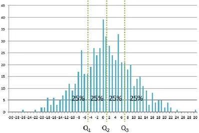
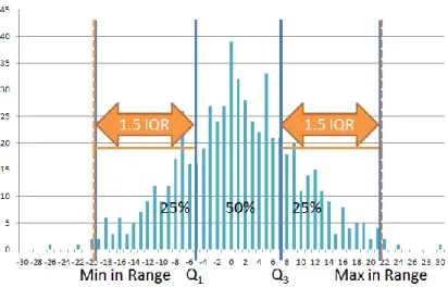
2.1.1. Quantiles and Quartiles ... 44
2.1.2. Univariate and Multivariate Distributions ... 45
2.1.3. Outliers ... 46
2.1.4. Data Variation (Noise) ... 49
2.2. Model Qualification ... 49 2.2.1. Cost function ... 50 2.2.2. Overfitting ... 50 2.3. Model Verification ... 52 2.4. Model Validation... 52 2.4.1. Cross-validations... 53 2.4.2. Holdout validation ... 54
2.4.3. Model Validation Summary ... 54
2.5. Model Selection... 54
2.5.1. Statistical Estimators ... 55
12
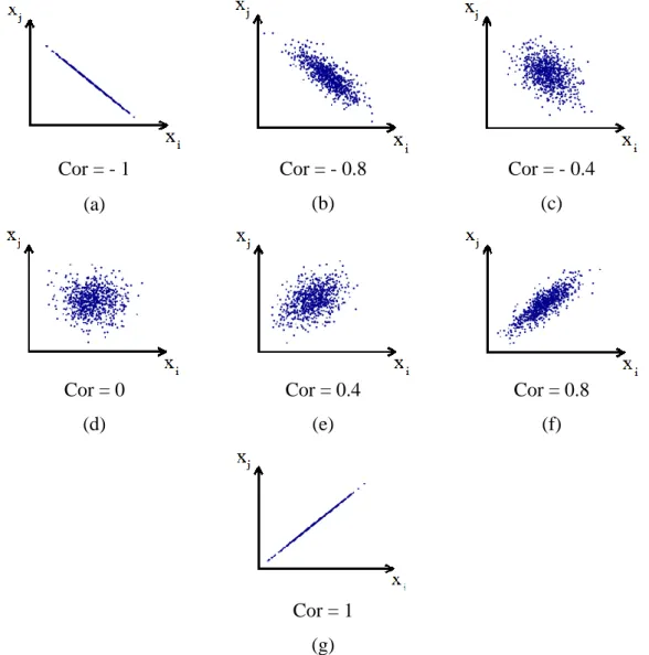
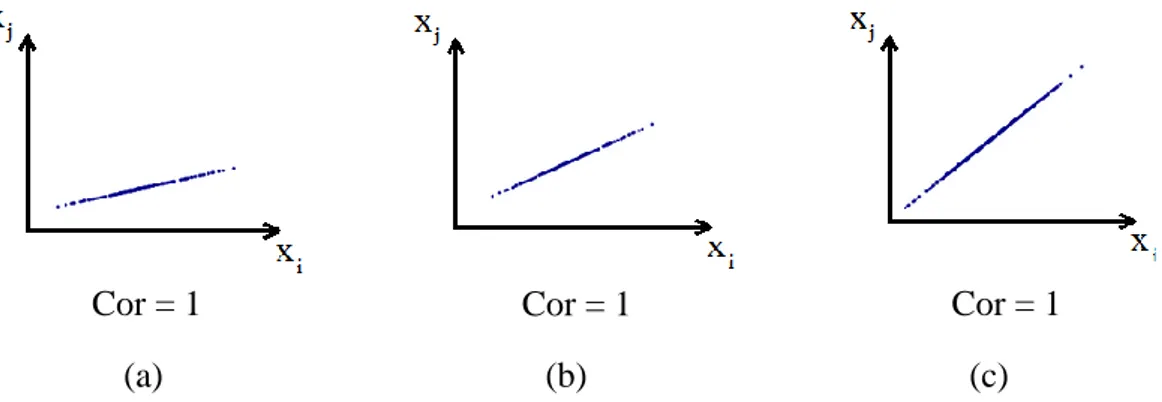
2.5.3. Correlation Matrix ... 61
2.5.4. Model Selection Synthesis ... 64
2.6. Conclusion ... 65
3. Sensitivity Analysis ... 69
3.1. General Steps for Performing Sensitivity Analysis ... 69
3.1.1. Specify the right output variable for the problem ... 69
3.1.2. Select the inputs of interest ... 70
3.1.3. Explore the input space ... 70
3.1.4. Evaluate the model for each sample set of input values ... 71
3.1.5. Apply an estimator of sensitivity to the output variable ... 72
3.2. Local Sensitivity Analysis ... 72
3.3. Global Sensitivity Analysis ... 73
3.3.1. Generate a sample of the inputs distributions: ... 74
3.4. Sampling Techniques ... 74
3.4.1. Sampling Evaluation Criteria ... 75
3.4.2. Sampling Strategies ... 78
3.5. Global Sensitivity Analysis Algorithms ... 85
3.6. Variance-based Sensitivity Analysis ... 87
3.6.1. First-order indices ... 89
3.6.2. Higher-order indices ... 89
3.6.3. Total-order indices ... 90
3.6.4. Example of Sensitivity Indices ... 90
3.6.5. Estimation of the Sensitivity Indices ... 91
3.7. Conclusion ... 98
4. Lithography Modeling ... 101
4.1. E-beam process characteristics... 101
4.1.1. Forward Scattering ... 102
4.1.2. Backscattering ... 102
4.1.3. Secondary Electrons... 102
4.1.4. Flare or Fogging ... 102
4.1.5. Acid Diffusion on Chemically Amplified Resists (CARs) ... 103
4.1.6. Etching ... 103
13
4.2.2. Exposure Simulation ... 107
4.2.3. PAG Simulation ... 108
4.2.4. PEB Simulation ... 108
4.2.5. Resist Development Simulation ... 109
4.3. Compact Models ... 110 4.3.1. Electron Scattering ... 110 4.3.2. Extreme-long-range Effects ... 118 4.3.3. Etching Model ... 119 4.3.4. Resist Model ... 120 4.4. Conclusion ... 124 5. Model Calibration ... 129
5.1. Compact Model Calibration for E-beam Lithography ... 129
5.1.1. Calibration Design ... 131
5.1.2. Verifying a Calibration Design ... 137
5.1.3. Building a Calibration Design ... 141
5.1.4. Impact of Process Variation ... 147
5.1.5. Calibration Layout Pre-correction ... 151
5.1.6. Calibration Layout for Extreme Long-Range Effects ... 152
5.2. E-beam Lithography Model Validation ... 154
5.3. E-beam Lithography Model Selection ... 155
5.3.1. Cost Function for e-beam modeling ... 155
5.3.2. Coefficient of Determination for e-beam modeling ... 156
5.4. Conclusion ... 159
6. Other Applications ... 163
6.1. Extreme-long-range Effects Correction ... 163
7. Results ... 169
7.1. Impact of Process Variability over Model Calibration ... 169
7.1.1. Experimental Variability Quantification... 169
7.1.2. Variability Impact over Model Calibration... 173
7.1.3. Summary ... 176
7.2. Model Calibration Use Cases ... 177
7.2.1. Gamma PSF ... 177
14
7.2.3. Calibration Using Only Pre-available Data ... 184
7.3. Extreme-Long-Range Calibration Results ... 190
7.4. Use of Cross-validation ... 193
7.5. Sensitivity Analysis Characteristics ... 196
7.5.1. Influence of dominating parameters over Sensitivity Analysis indices ... 196
7.5.2. Impact of the pre-correction on the Sensitivity Analysis... 197
7.5.3. Sensitivity Analysis and the Range of the Parameters... 198
Conclusion ... 203 Glossary ... 206 Publications ... 209 Papers ... 209 Patents ... 210 References ... 211
Annex I - Lithography Characteristics Metrics ... 225
Annex II - Exposure Compensation ... 229
15
Introduction
“In the strict formulation of the law of causality—if we know the present, we can
calculate the future—it is not the conclusion that is wrong but the premise.”
17
Introduction
Since the development of the first integrated circuit, the number of components in a chip continued to grow and the dimensions of each component continued to be reduced. These two effects combined give rise to impressive improvements in system performance. Reducing the size of transistors improves their performance [DENNARD 1974]. Moreover, adding more transistors to the same circuit increases its capacity for arithmetic and logic operations as well as its memory. As the integrated circuits became more powerful and versatile, more sectors of the industry started employing them in order to improve their own products. Nowadays, even equipment as simple as coffee machines and dishwashers may present a few integrated circuits, while complex ones, such as cars and airplanes, may present from hundreds to thousands of chips.
The economic model of this apparently ever expanding market relies on achieving and maintaining a given pace when it comes to higher circuit integration. This pace is well known in the industry as the Moore’s law. In its most common definition, Moore’s law predicts that the number of transistors in a chip would double every two years [MOORE 1975]. In another formulation it says that computer performance would double every eighteen months. This last formulation, although very common, was never stated by Moore [MOORE 1995]. Eventually, many other predictions stating that something would double every eighteen or twenty four months have been called Moore’s law as well.
In his original formulation [MOORE 1965], the Moore’s law predicted that the number of components in an integrated circuit would double every year. Figure 1 (a) shows the graph used originally by Moore indicating the number of components in a chip from 1959 to 1965 and the estimation for the next ten years (according to the Moore’s law). In 1975, Moore changed his law [MOORE 1975] for expecting the doubling every two years, instead of every year, as he expected that most of the innovating possibilities on how the relative component distribution could be improved were already made, as shown in Figure 1 (c). It is interesting to remark that in the ten years that separate both publications, the number of components roughly double every year, as presented in Figure 1 (b). Moreover, right after the second publication, the number of components doubled every two years, exactly as predicted again by the 1975 Moore’s law.
Therefore, this behavior allowed the industry to sell more powerful chips for the same price or to reduce the price for the same chip. This business model has being working very well while the fabrication technology allowed to continually scale down the circuit components. Since the entire economic model of this industry relies in Moore’s law, it may even be seen as a self-fulfilling prophecy.
18
(a) (b) (c)
Figure 1 (a) presents the original prediction from Moore’s work in 1965 [Moore 1965]. (b) shows the data until 1975, indicating that the first prediction was right [Moore 1975] and (c) shows the inflection point where Moore predicted
the law change from doubling every year to doubling every two years [Moore 1975].
For each new technology node proposed by the industry, the complexity of the fabrication process increases to deal with the increasing constraints due to its scaling down. Hence, each new process of fabrication of integrated circuits requires a larger number of steps, which are all being constantly improved in order to achieve the requirements for component scaling down. Among these steps, lithography is one of the most critical for miniaturization due to the tightened requirements in both precision and accuracy of the pattern dimension printed into the wafer. Therefore, the lithography process is one of the pillars of the entire business model of the semiconductor industry due to its direct relation with achieving the scaling down required by the Moore’s law.
There are several different lithography techniques. The technique used in mass production is optical lithography or photolithography. It is favored by the industry because it presents the throughput and resolution required by today’s technology at the best cost. This technique is based on using a photomask, which is a transparent plate with opacities that allows writing the circuit by either letting the light pass or blocking it, patterning the design in a photoresist. The quality of the patterns present in the photomask is directly proportional to the quality of the photolithography resolution. In integrated circuit fabrication processes several masks are used, at least one for each layer of the circuit. For the most critical layers (i.e. the ones presenting very small features, high density or requiring highly controlled dimensions), the masks are written using an electron beam (e-beam) machine, which presents high accuracy and precision and the resolution required for writing such critical patterns.
Nevertheless, nowadays optical lithography is facing resolution limitations and, in order to continue to shrink components dimensions, the industry is looking for a better solution. Some of the candidate solutions are Multi-patterning (MP), Extreme-Ultra-Violet (EUV) lithography, Direct Write (DW), Nano-imprint and Direct Self-Assembly (DSA). Although these alternatives present significant differences among each other, they all rely on e-beam writers at some point of their flow. This makes of e-beam machines a meeting point for the future of lithography.
E-beam writers present high accuracy, but they are subject to phenomena that limit their resolution as well. The beam presents a diameter which is not negligible; some of the electrons
19
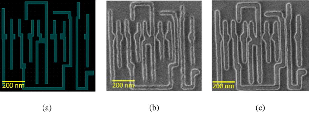
scatter while interacting with the material and may expose regions that were supposed to be left unexposed. Electrons leaving the surface of the material may be reflected back to any other spot and so on. These effects, combined with other factors such as resist development and plasma etching characteristics directly impacts the resolution of the patterns written by e-beam machines. Besides the natural approach of working in improving these machines, the solution the industry adopted to address these effects is to predict and compensate for them. Traditionally, this compensation is called Proximity Effect Correction (PEC), although it may account for several different factors. Nonetheless, this correction requires predicting the effects, which is achieved through modeling. Figure 2 illustrates the importance of developing accurate models for e-beam processes. Figure 2 (a) shows a pattern to be printed, while in Figure 2 (b) one may see a low quality result due to poor compensation and Figure 2 (c) shows a much better result, after proper compensation.
(a) (b) (c)
Figure 2 (a) presents a pattern to be printed, (b) a SEM picture of the same layout after exposure based on compensation of a poor model and (c) a SEM picture of the same layout after compensation using a better model.
E-beam modeling has being developed together with the first e-beam machines. However, as technology advances, the requirements of modeling accuracy are getting tighter. To respond to it, the models are also becoming more complex. The model calibration effort is therefore increasing and the impact of every small change in the writing process has to be directly reflected in the model being used. In this new scenario, new models and strategies for calibrating them are continually being proposed.
The main goal of this thesis is to provide a complete flow on how to create an accurate and useful model for e-beam lithography both for simulation and for correction. In the process of describing such flow, most of the key aspects that contribute to the e-beam processes are described. Moreover, some of the strategies for determining the best model for a given process and for selecting the best test patterns to be used in an experimental calibration are also described. State-of-the-art e-beam models are discussed and their weaknesses exposed to finally present new model structures that enables continue to advance to future technology nodes using current process flows.
Chapter I presents the basic concepts of the semiconductor industry, mainly focusing on integrated circuit fabrication and the aspects of the lithography. The most prominent candidate
20
lithography techniques to be used in future technology nodes are also discussed and their weakness and strengths are pointed out.
In chapter II the aspects of producing, validating and comparing models are presented. Basics on data analysis are also discussed to be employed in the evaluation of the model calibration process. Special attention is given to the criteria to evaluate the quality of a model, presenting different statistical algorithms for performing biased, unbiased and robust evaluations.
The chapter III presents the concepts of Sensitivity Analysis in both their local and global forms. More emphasis is given to Variance-based Sensitivity Analysis since it is the more suitable approach for the applications required in this thesis. Sampling techniques and evaluation criteria are also presented and discussed. Although general information are presented, the focus is on the aspects necessary for the further development of the work of this thesis.
Chapter IV describes the characteristics and issues of e-beam lithography and stresses the necessity of modeling them. Moreover, strategies for modeling e-beam lithography both using first principle models and compact ones are discussed and new compact models are proposed in order to obtain higher precision than the state-of-the-art of the industry.
The chapter V focus on the model calibration, either relying in first principle model results or, especially, relying in experimental data, which is becoming the industry standard. Moreover, the aspects related to generating and verifying a design to be used in the experimental calibration procedure are discussed. The strategy to ensure a calibration design that is suitable to the aimed process models and is robust to the variability of the process is detailed. Finally, the optimum strategies to validate the generated lithography model are presented.
In chapter VI another application developed in the period of this thesis is presented. It consist of an strategy to compensate for extreme-long-range effects on large data, such as processing the entire reticle (for mask writing) or the entire wafer (for direct write). This is performed based on a density evaluation and performing the convolution of the generated model over the density map instead of over the original data.
Chapter VII presents the results of employing the techniques discussed in this thesis for e-beam modeling. The results of model calibration exercises over the results of first principle models and experimental data is presented. Moreover, some specific topics regarding sensitivity analysis were evaluated and are discussed as well. The evaluation of a model using cross-validation is also presented, as well as a study showing the impact of process variability over the calibration result. Finally, a result of the evaluation of the extreme-long-range impact over the direct-write exposure.
Finally, the last chapter of this work presents the conclusions and perspectives for continue to improve the performance of e-beam exposures using prediction and compensation in order to address future technology nodes.
21
Chapter I. Basic Concepts
“The future influence the present just as much as the past.”
23
1. Integrated Circuit Fabrication
The fabrication of integrated circuits (ICs) is a multiple-step sequence during which circuits are created on a wafer made of semiconducting material. A typical state-of-the-art wafer is a circular slice about 0.75mm thick and 300mm in diameter. The most frequently used wafer is silicon, but some other approaches exist, notably the Silicon on insulator (SOI). The steps for producing the circuit on a wafer are divided into Front-End-of-Line (FEOL) and Back-End-of-Line (BEOL). FEOL is where the individual devices – such as the transistors – are patterned in the semiconductor. The BEOL is responsible for interconnecting the devices created during the FEOL. Generally it begins when the first layer of metal is deposited on the wafer. BEOL includes contacts, insulating layers, metal layers and goes up to the bonding sites for packaging.
During both FEOL and BEOL, each step of adding a new material layer requires at least three steps, which are the deposition, the patterning and the removal. Deposition consists in growing, coating or transferring a material onto the wafer by technologies such as physical vapor deposition (PVD), chemical vapor deposition (CVD), among others. Patterning consists in shaping or altering deposited materials. The removal step consist in removing material from the wafer, by processes such as etching or chemical-mechanical planarization (CMP). After these three steps, a resist strip is performed to prepare the material for the next process. Figure 3 illustrates the steps of this flow.
Figure 3. Microelectronic process for one layer patterning.
1.1.
Lithography Process
As mentioned in the previous section, a chip is composed of several layers and, for patterning each layer, it is necessary to perform one or more lithography steps. There are several different strategies to transfer the patterns of a circuit into the silicon wafer. Nonetheless, the industry current standard is photolithography.
24
1.1.1. Photolithography
Photolithography is the process where a light-sensitive polymer, called photoresist, is exposed and developed to form 3D patterns on the substrate. Ideally, the final image found at the photoresist is identical to the intended pattern. The local exposure of the photosensitive polymer is achieved through a photomask. This mask is a quartz plate presenting opaque and transparent features either blocking the light or allowing it to shine through. The intended patterns to be exposed in the substrate are, therefore, first drawn on the mask and, then developed on the substrate. The process of writing the intended patterns on the mask is very similar to a lithography process itself for a single layer and usually relies on laser writers or electron-beam writers (details on electron-beam lithography are presented further on this chapter). Usually patterns present in a mask present a scale factor in comparison to the final dimensions expected on the wafer. In state-of-the-art industrial production, patterns on a mask are four times bigger than the desired dimensions on wafer.
Figure 4 (a) represents a simplified scheme of a photolithography exposure tool while (b) shows the five main steps of the lithography process, from coating the resist to the development of the intended pattern on the wafer.
(a) (b)
Figure 4. (a) Simplified scheme of a photolithography exposure tool while (b) shows the five main steps of the lithography process.
The resolution of this system is limited by the wavelength of the light used and the ability of the projection lens system to capture enough diffraction orders after passing through the mask. Lithography systems have progressed from blue wavelengths, 436nm, to ultraviolet (UV),
25
365nm, and to deep ultraviolet (DUV), 248nm, and finally state-of-the-art photolithography tools employ (DUV) light with a wavelength of 193nm combined with immersion fluid.
The minimum feature size that an optical projection lithography system can achieve may be approximated by the so called Rayleigh formula (1).
𝐶𝐷 = 𝑘1𝜆 𝑁𝐴
(1)
Where CD is the critical dimension, or the minimum size of feature that may be exposed by the tool, λ is the wavelength of the light employed by the tool, NA is the numerical aperture of the lens from the wafer perspective and k1 is a coefficient that lumps several process-related factors and is larger or equal to 0.25.
The numerical aperture is computed as shown in (2) and it is a convenient way to describe the size of the lens aperture in the lithography system. NA value for optical lithography DUV 193i is 1.35 while for extreme ultraviolet (EUV) it is 0.25 or 0.33 [ITRS, 2013].
𝑁𝐴 = 𝑛 sin 𝜃𝑚𝑎𝑥 (2)
Where θmax is the maximum half-angle of the diffracted light that is able to exit the objective lens while n is the refractive index of the medium between the wafer and the lens.
According to this equation, the CD may be decreased by increasing the numerical aperture and/or by reducing the wavelength. However, another major concern of this system is the depth of focus (DoF), which is the tolerance of height placement in the image plane in relation to the lens. The depth of focus can be approximated by (3).
𝐷𝑜𝐹 = 𝑘2𝜆
𝑁𝐴2 (3)
Where k2 is another coefficient that lumps several process-related factors.
Photolithography end has been predicted in many occasions but has continually advanced in order to address pattern sizes that fulfilled ITRS targets to meet Moore’s law. For instance, years ago it was supposed to be impossible to write features smaller than 1µm by an optical strategy. More recently, another barrier was broken when features smaller than the exposure wavelength were also printed successfully using photolithography. Nowadays, once again, photolithography seems to have reach a hard point. The project to increase the resolution limits by using 157nm wavelength failed due to technical and economic problems. Last significant improvement in this system was the adoption of the immersion technique for 193nm steppers.
Immersion lithography is a technique that replaces the air in the gap between the final lens and the wafer surface by a liquid with a refractive index greater than one. Increasing n increases the numerical aperture NA, as seen in (2).The improvement in resolution is by a factor of the refractive index and, today, the industry employs highly purified water, whose index is 1.44 at a wavelength of 193nm. Moreover, this approach may be used to improve the DoF by at least
26
the refractive index of the fluid and by larger factors as the pitches become smaller [MACK, 2007].
Therefore, the industry continues to look for solutions to achieve smaller technology nodes. Currently solutions are benchmarked to manufacture the 14nm node, which is likely to require a new breakthrough on the lithography process. On the next section some candidate solutions for becoming the industry main stream lithography technique are presented.
1.2.
Candidate Lithography Processes
The industry have been improving the lithography processes by reducing the wavelength. This trend stopped at 193nm. The strategy of choice to continue evolving was the 157nm wavelength, which appeared in both ITRS and Intel [SILVERMAN, 2002] roadmaps as the replacer of the 193nm. However, in spite of the large investment and the advances achieved, it was eventually abandoned for good in favor of the immersion lithography approach (193i optical lithography).
When the 193i reached its limits, the industry continued looking for a long term solution. The approach of choice for a long time has been the Extreme-ultraviolet (EUV) lithography at 13.5nm wavelength. This approach has being in roadmaps as a future technology even before the use of immersion [SILVERMAN, 2002] but is still lacking some advances to overcome its current limitations. Meanwhile, other approaches were proposed, such as the Direct Write (DW) using electron-beam (e-beam) machines, nanoimprint and, more recently, multiple-patterning and direct-self-assembly (DSA). Yet the industry seems to be already employing multiple-patterning to achieve the 28nm and 22nm technology nodes [ITRS 2013].
A summary of each lithography strategy and its capabilities for reaching the CD and pitch values are given in Table 1 [ITRS 2013]. The black cells indicate where there are published papers indicating the use of the technique in production, grey cells and cross hatched ones indicate where techniques have been demonstrated to be capable of smaller resolutions.
Table 1. Demonstrated Line and Space Resolution of Potential New Patterning Techniques (from Figure LITH1A of ITRS 2013)
27
Observe that Double Patterning (Immersion SADP) and Quadruple Patterning (Immersion SAQP) are in production for achieving CDs of 18nm and 16nm. While the 14nm node is still only demonstrated as possible but there are several approaches that may reach such resolution (Quadruple Patterning, EUV with Double Patterning, Nanoimprint or approaches based on DSA).
1.2.1. Extreme-ultra-violet (EUV) Lithography
Photolithography has been advancing in the past decades by reducing its wavelength in order to improve its resolution. As the wavelength becomes smaller, it is difficult to obtain non-absorbing materials to be employed as optics of the lithography systems. Most of the light gets absorbed by the lenses. Nonetheless, a strategy was proposed in order to drastically reduce the wavelength, known as Extreme-ultra-violet (EUV) lithography [BAKSHI, 2009].
EUV wavelength is around 13nm, for which no set of transparent masks can be obtained. Therefore, EUV lithography relies in reflection through mirrors in order to draw the images on the wafer. Reflection occurs at interfaces between materials of different indices of refraction. The larger the difference of the indices of these two materials, the greater the reflectivity of their interface. However, at wavelengths such as the ones of EUV, all materials present indices of refraction around 1. Thus, it is difficult to create a highly reflective interface. Nonetheless, by using multilayers alternating high-Z (chemical elements with a high atomic number) and low-Z (chemical elements with a low atomic number) materials, it is possible to obtain mirrors with reflectivity in the range of 60-70%. Basically, it is the accumulation of interfaces of small reflectivity that allows reaching reasonable total reflectivity, if a sufficient number of layers is employed.
Besides the criteria of being high-Z and low-Z materials, the chosen materials must also be weak absorbers of EUV light. This is because the light must be able to penetrate to the lower layers of the film stack. Some stacks have been identified and the industry tends to use pairs of Molibdenum (Mo, Z = 42) and Silicon (Si, Z = 14) for the multilayer reflector at 13.5nm. This stack is usually called the MoSi stack.
Another significant change from 193i lithography is the change in the absorber material used in the mask. For EUV, Cr is no longer sufficient and heavier materials, such as the Ta, are used instead. An example of the difference in the materials stack for a photolithography mask and a EUV mask is presented in Figure 5. Observe that EUV requires more layers and heavier materials, which have impact on the mask writing procedure, topic that will be further explored later in this thesis.
28
Figure 5. An example of the stack of materials for a photolithography mask and a EUV mask.
Using mirrors instead of lenses requires changes in the exposure tool as well. Figure 6 shows a schematic of a EUV tool with its sets of mirrors and the reflecting mask.
Figure 6. A simplified representation of the EUV exposure system.
However, since at its best each mirror (and the mask itself) absorbs 30% of the energy of the EUV light, the original energy at the source must be extremely high in order to compensate those losses. If the amount of energy on the wafer is low, the exposure must continue for a longer period, increasing significantly the writing time of the wafer. Current requirement is 150W of EUV light at intermediate focus [BAKSHI, 2009]. This is being one of the most significant limitations to achieve production level in the industry using EUV.
Finally, EUV lithography tools must be under vacuum in order to avoid photons absorption. Hence a new technical difficulty appears during exposure of photoresist due to resist outgassing and molecule cracking under EUV. This cracking induces amorphous deposition onto mirrors, reducing significantly the reflectivity continuously.
Since EUV failed to be ready to replace 193i in time for the technology nodes using pitch below 80nm, the industry found a fallback plan in using multiple-patterning as a strategy to relax some of the constraints of 193i optical lithography. This is the topic of the next section.
1.2.2. Multiple-patterning
The physical limitation of the optical lithography is not the size of the features alone but the association of this dimension and the space close to it. This constraint is usually represented by the notion of pitch. Since, after the Rayleigh criterion, the resolution limit of standard 193i is close to be the 90nm pitch, the industry found in multiple-pattering the strategy to continue to
29
operate with most of the same process flow of the 193i and achieve technology nodes of 28nm and below [FONSECA, 2009][OWA, 2014] [MAILFERT, 2014].
There are several variations of this approach, either relying in a single exposure (and, therefore, in a dual-tone photoresist or a dual-tone development, for instance) or in multiple exposures (using a single or multiple resists). Although using a single exposure has the advantage of not increasing the number of masks required for drawing the intended patterns, the complexity added to the process by modifying the resists or developments makes them hardly viable for industrial applications.
Multiple exposure is based on the strategy of separating a layout into different masks in order to reduce the feature density on each exposure. The decision of which patterns should be drawn in which exposure, usually called split, is usually performed automatically by graph coloring algorithms [MAILFERT, 2014]. Relaxing the pitch allows to print correctly very small features. Figure 7 shows a representation of patterns to be exposed and the points where the pitch should be relaxed (distance violation). It also shows the coloring result and the two resulting masks (first mask with the features from coloring group A and second mask with the ones from coloring group B) for a double exposure procedure.
Figure 7. A representation of the partition of the patterns to expose in order to prevent the violation of the minimal distances. The coloring and the resulting two masks.
However, not all patterns are printable using a double exposure approach as presented in Figure 7. In some configurations more than two colors are necessary, as the example shown in Figure 8.
30
Figure 8. A representation of the partition of the patterns to expose in order to prevent the violation of the minimal distances and the impossibility to define the two colors and remove all violations.
The issues of coloring such as the one presented in Figure 8 may still be addressed by only two layers if one employs a pattern splitting technique, for instance. However, dividing lines increase the registration criticality and also works as a resolution limitation of this approach.
Although quadruple exposures [OWA, 2014] are a reality and even more exposures are feasible in order to further relax the half-pitch constraint, this approach is not viewed as an ideal candidate solution by the industry, (at least not for several layers). The reason for that is mostly related to the cost of producing so many masks and having so many process steps (after all, the Moore’s law is about economics, not physics). Moreover, challenges of alignment as the number of exposures increases drastically. Due to these limitations, the industry is still looking for other solutions in order to continue evolving from one technology node to the next. Since EUV is still late, in the past few years another solution has increase attention due to its small feature sizes and the fast advances obtained by research groups. It is known as Directed self-assembly (DSA).
1.2.3. Directed self-assembly (DSA)
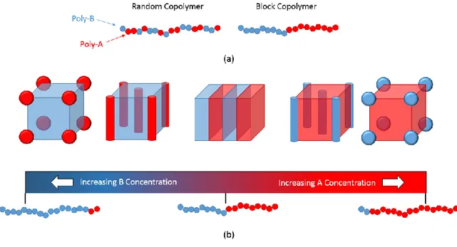
The Directed self-assembly (DSA) approach relies on inducing alignment in sets of block copolymers to organize themselves in a directed way in order to create regular structures [TSAI, 2013][JEONG, 2013]. The base of DSA are the block copolymers, which present two different polymers in blocks instead of randomly distributed in a chain, as represented in Figure 9(a). According to the relative distribution of each polymer, the way they interact may turn in different organized structures, as shown in Figure 9(b).
31
Figure 9. Basics on copolymers for DSA. (a) shows the difference of a random copolymer and a block one while (b) shows the difference in concentrations.
The dimensions in this approach are controlled by the molecular size and not by any diffraction parameter. Nonetheless, the ability to control the way how the molecules will place themselves is delicate. There are two main approaches to control the orientation of the molecules, namely graphoepitaxy and chemical epitaxy. The first relies on pre-existing topographic patterns generated by a standard lithography process with relaxed constraints while the second relies on surface patterns presenting a selective surface modification. Figure 10 shows an illustration of the difference between (a) the graphoepitaxy and (b) the chemical epitaxy approaches.
(a) (b)
Figure 10. Schemes for (a) graphoepitaxy and (b) chemical epitaxy.
Independently of the approach used, if the procedure is well succeeded the result is a very regular periodic structure. In order to convert the generated patterns into portions of real circuits it is necessary to remove some of the structures by using another lithography step. This step present more relaxed terms of density than if it was employed directly to generate the features itself, but still requires high accuracy and small dimension. This final step is usually performed using either photolithography employing a cut-mask or using electron-beam lithography. Figure 11 illustrates this process.
32
Figure 11. Example on how a procedure to remove some of the structures from the DSA in order to form the intended patterns.
Although DSA is a very promising approach and the industry is paying closer and closer attention to its development, it is still far from being a mature approach to be employed for future technology nodes. One of the main issues of this approach is the defectivity issue, which affects drastically the yield of this kind of lithography. In this sense the industry also looks for the direct-write approach using e-beam machines, which is the topic of the next section.
1.2.4. Electron-beam lithography
Electron-beam (e-beam) lithography has been known since the sixties. Its origins report to microscopy in which, by using electron sensitive resists, it was possible to employ the focused beam of electrons to draw custom shapes. In opposition to what is observed in the photolithography, most of the e-beam lithography techniques do not require the use of masks, being, on these cases, known either as maskless lithography or as direct write lithography [LEE, 1981][CRAIGHEAD, 1983].
The interest in employing electrons instead of photons to perform exposure comes from its high resolution. While photons wavelength for lithography are stalled at 193nm, the electron wavelength is of around 0.05 Å (or 0.005nm) at 50keV, disregarding the relativistic effects [MARTIN, 2011]. This very small wavelength makes the diffraction effects negligible.
1.2.4.1. Gaussian electron-beam lithography
The first and simplest strategy of e-beam lithography is based on Gaussian beam. A Gaussian e-beam tool usually employs a heated lanthanum hexaboride (LaB6) submitted to a very high voltage (several thousands of volts) as electron source. A column composed of several electromagnetic lenses condenses the electrons into a beam and allows it to focus into a given point of the wafer. Other lenses allow the beam to be deflected in order to draw the intended patterns. Figure 12 (a) shows a simplified example of such e-beam machine. This approach is called Gaussian beam due to the
33
scattering effect of the beam that distributes the incident electrons in a Gaussian probability around the focal point.
(a) (b)
Figure 12. (a) A simplified representation of the Gaussian e-beam column and (b) The intended pattern being exposed by a Gaussian e-beam.
Using this strategy, the beam diameter may be smaller than 10nm [DIAL, 1998], [KURIHARA, 1995], [YAMAZAKI, 2000]. This dimension is inferior to the smaller features aimed for the industry in today’s and near future technologies.
As the generated beam has a fixed shape and dimension, the intended patterns to be exposed are divided into very small features in a process called pixelization. In opposition to the photolithography, which expose an entire mask at once, the Gaussian beam lithography exposes one pixel at a time. This sequence of exposure is represented in Figure 12 (b). Even if it could be possible to increase substantially the time for exposure each pixel, the final exposure time using a Gaussian e-beam approach would still be way much slower compared to the photolithography. This is why this approach is not used in mass production of ICs and is mostly restricted to research.
Nonetheless, the electron lithography presented a series of advantages. One of them is the simple fact that a mask is not necessary to control the exposure so all the cost and challenges related to it are avoided. Instead, a software controls the exposure based on an input file. It also gives flexibility to the system as the files can be changed easily in contrast of a mask that, once printed cannot be modified.
In order to improve the throughput of the Gaussian e-beam strategy, a new type of electron exposure was proposed, called shaped electron-beam lithography.
34
1.2.4.2. Shaped electron-beam lithography
One of the approaches proposed by the industry to improve the throughput of the electron lithography was the shaped electron-beam [RISHTON, 1999]. This approach relies on shaping the beam (hence its name) to cover a given geometric area on the target. In order to produce the shapes, the machine structure is very similar to the one used for the Gaussian beam but with the addition of shape aperture plates that control and give the desired geometry to the beam. A representation of the column is presented in Figure 13(a).
The geometry of the beam may vary in shape and size according to the ones available by the combination of the aperture plates present in the machine but, in general, may cover hundreds of points drawn by the Gaussian beam all at once. A scheme of a sequence of printing a pattern is represented in Figure 13(b). Observe that the intended pattern is exposed in three shots instead of the large number of dots presented in a Gaussian beam exposure (as shown in Figure 12 (b)).
Although considerably improving the exposure time of the Gaussian beam approach, this method is not fast enough to achieve the throughput required by IC mass production, which is usually stated as 100 wafers per hour (WPH). Current throughput of state-of-the-art shape beam is around 0.1 WPH [PFEIFFER, 2010]. Although its speed is a thousand times slower than the requirements for direct write, it is sufficient to be used as a method for mask writing for the photolithography. For this reason, the shaped e-beam lithography is the tool employed by the industry to write masks for 193i lithography, for EUV lithography and in all strategies of multiple patterning. However, as the technology advances, the structures become more complex due to more complex compensations for light diffraction and the mask writing time is becoming a concern for using shaped e-beam lithography.
35
(a) (b)
Figure 13. (a) A simplified representation of the shaped e-beam column and (b) The intended pattern being exposed by a Gaussian e-beam.
In order to further improve the throughput of electron-beam lithography the industry proposed to build arrays or matrices of beams (or shaped-beams) in order to expose a larger surface at once on the wafer. This approach is known as multi-beam and is discussed in the next section.
1.2.4.3. Multi-beam
To address the throughput limitations of e-beam writers the industry proposed recently the use of multiple beams in parallel, in a strategy known as multi-beam. There are two main variants of this approach, one presenting several beams in the same column and the other presenting several columns with one beam per column. The beams used can be either Gaussian (IMS Nanofabrication and MAPPER lithography) or Shaped (Vistec), the latter achieving little commercial success as of today. Another important difference among the strategies is the energy employed. While most of the approaches rely on high energy (around 50keV or 100keV), MAPPER adopted a “low” energy approach of 5keV. In any case, the throughput of these machines are increased by the parallel writing of all the beams, which may be used either for writing masks or even proposing to reach the performance required for direct write.
Generally speaking, the strategy splits a single beam in a large number (reaching thousands or even hundreds of thousands) of smaller beams. The number of beams vary from one implementation to another, as MAPPER FLX1200 announces 13,260 electron
36
beams in its production machine [BRANDT, 2014] while IMS Nanofabrication mention 262,144 programmable beams in their eMET [PLATZGUMMER, 2013].
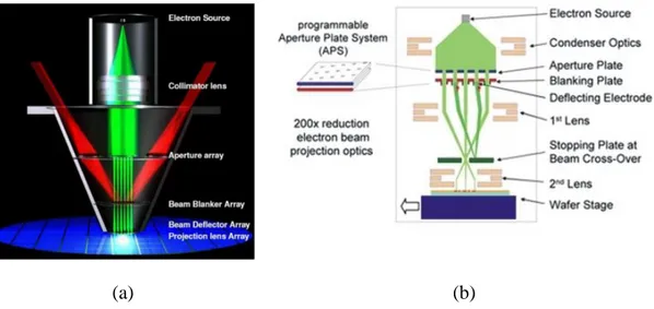
These beams scan the entire surface of the wafer or mask by the movements of the stage, while being turned on or off according to the requirements of the intended patterns. Since the entire surface is scanned independently if there are patterns to expose or not, the exposure time is no longer a function of the complexity of the patterns being exposed, qualifying this approach for complex mask writing for future nodes. Figure 14 shows the schematics of the tools proposed by (a) MAPPER and by (b) IMS Nanofabrication.
(a) (b)
Figure 14. Schematic principles of the multi-beam columns from the tools proposed by (a) MAPPER and (b) IMS Nanofabrication
Other alternatives using multiple columns with one or several beams per column have also been proposed. Vistec Multi Shaped Beam (MSB) proposed a structure where each column contains a tool able to generate a Shaped Beam [STOLBERG, 2010]. Figure 15 shows an illustration of such structure.
(a) (b)
Figure 15. Schematic of (a) single variable shaped beam and (b) multi shaped beam technique, from [GRAMSS, 2010]
37
Another approach is employed by KLA-Tencor with its tool REBL [PETRIC, 2009a], [PETRIC, 2009b]. The main difference of this approach is that it is based on reflection. A large electron beam is projected over an electrostatic mirror matrix, each mirror being responsible for reflecting one pixel of the target image. Each mirror works like a blanker controlling the behavior of a single beam. The exposure is performed at several wafers at the same time by either a rotating stage (as shown in Figure 16 (a)) or a linear stage (as shown in Figure 16 (b)).
Figure 16. Schematic representation of the reflective tool REBL from KLA-Tencor
In comparison to the writing strategies of Gaussian-beam and Shaped-beam, the multi-beam approach writes several pixels (as in multiple Gaussian-multi-beam) or several shots (as in multiple shaped-beam) at once. Figure 17 shows a graphical representation of the sequence of exposure of a multiple Gaussian-beam tool. Refer to Figure 12 (b) to compare with the standard single Gaussian-beam approach.
In any case, the multi-beam approach is still dealing with some important issues in order to be used by the industry. Notably, the exposed surface is heated due to the large number of beams reaching the same area at the same time and the beam placement is difficult to achieve accurately to control the dose received at each point. Moreover, another critical issue is the handling of such large volume of data due to pixelating the intended patterns, requiring a large data bandwidth.
Another approach considered by the industry to provide acceptable throughput in the lithography process, especially for regular designs such as memories, is the nanoimprint lithography (NIL). It is described in the next section.
38
Figure 17. The intended pattern being exposed by a multi-beam exposure tool
1.2.5. Nanoimprint lithography (NIL)
Nanoimprint lithography (NIL) has emerged as a candidate solution for next-generation IC manufacturing for its advantages for mitigating the limitations of both photolithography and e-beam lithography. Thereby, nanoimprint comes with a promise of high-resolution as it does not suffer the diffraction issue that limits the photolithography and high-throughput in comparison to the e-beam lithography [CHOU, 1996][TORRES, 2003].
Basically, there are two main nanoimprint strategies: thermal imprint and UV-imprint. The first process consists in heating a thermoplastic polymer above its glass transition temperature, enabling the material flow to fill the structures of a mold. After, the temperature is lowered until the replicated patterns are solidified in place. Finally, the mold is removed. The UV-imprint employs an UV-curable monomer as compliant polymer layer in order to enhance fluidity of the printed material. The monomer layer is imprinted and submitted to broadband UV light radiation in order to form a rigid polymer. This enables the imprint pressure to be significantly reduced and avoid the time consuming and stress induced by a high temperature cycle. Figure 18 presents generic views of the (a) thermal nanoimprint and (b) UV-imprint lithography flows.
The mold is usually made of quartz or silicon, which is patterned by any conventional lithography technique. Usually e-beam lithography is preferable due to its higher resolution whenever the nanoimprint aims to achieve the requirements of advanced technology nodes.
39
Figure 18. An illustration of the (a) thermal nanoimprint and (b) UV-imprint
Although nanoimprint is continually progressing, there are some issues that must be addressed. Adhesion between stamp and resist is an issue since the remains of the resist on the mold degrades pattern, reduces yield and damages the mold. Another critical issue is the life time of the mold. For the thermal nanoimprint, the changes of temperature and the high pressure cause stress and wear on molds and anti-sticking coating. This stress also presents a problem of alignment while using nanoimprint for multi-layer fabrication. Moreover, the viscosity of embossed material is an important issue, which may be a limiting factor for minimizing pattern dimensions and increasing pattern density. For UV-imprint, reactive species are generated during the light exposure. These species attack the anti-sticking layer of the mold so after a given number of imprints the mold must be cleaned to maintain sufficient demolding efficiency.
1.3.
Lithography Process Comparison
It is not clear which technique will be selected to be the next lithography process. It is highly probable that different applications or different layers will use different strategies, as their benefits are sometimes complementary and the constraints are different. Multiple-patterning is the approach in use by the industry to continue to advance and a multiple-patterning EUV approach is already being discussed for the near future. Multi-beam machines are in different stages of development and are likely to increase in importance for writing the masks for the new strategies based in light and the molds of nanoimprint lithography (NIL). Nanoimprint is a strong candidate for very regular structures such as memory circuits while DSA is still in an early stage of development to evaluate how it will impact the future technology nodes lithography strategies.
40
Nonetheless, a clear aspect that is shared by all approaches is that they benefit from using e-beam exposure at some point on their flow, as summarized in Table 2.
Table 2. The different next generation lithography candidate approaches and where e-beam tools are used on their flows.
Strategy Mask E-beam tool used?
193i multiple patterning Yes, more than one per
complex layer Yes, to the mask writing
Extreme-ultra-violet lithography
Yes, reflective with complex
stack Yes, to the mask writing
Directed self-assembly Probably, for guiding structures and for cut-mask
Yes, to write the guiding structures and cut masks or for directly cutting the patterns Multi-beam Direct Write No, write the intended
patterns directly on the wafer Yes, to the wafer writing Nanoimprint No, use a mold to print the
intended patterns on the wafer Yes, for writing the mold
1.4.
Conclusion
In this chapter it was shown that the current industrial technique for lithography (193 immersion optical lithography) is close to its limits and the industry is looking for a new approach. In order to mitigate the late availability (if ever) of EUV, the trend is to work with multiple patterning, which is already in production today for advanced technology nodes such as 18nm. However, this method presents its own limitations and is not able to provide, alone, a definitive answer for the technical and financial constraints faced by the industry for technology nodes below 14nm. Other strategies such as e-beam direct write using multi-beam technology and the directed self-assembly (DSA) approach are likely to be integrated to the flow for future technology nodes (either 10nm, 7nm or beyond). For some specific applications, such as memory chips, NIL is also a serious candidate to be used in future technology nodes. Nonetheless, it was shown that e-beam machines are the assembly point of all these alternatives, either as the main exposure tool or as the tool used to write the masks for DSA or optical lithography.
As e-beam machines seems to be down the road in any of the future strategies and even as the work horse for mask writing in current technology for the critical layers, it is imperative to understand the compensate for its limitations in order to achieve better resolution. Moreover, other factors that also limit resolution, such as etching bias and acid diffusion, must be addressed as well. The first step to compensate for these phenomena is the ability to understand, describe and predict the results of the lithography process. As these phenomena are more and more complex, the best manner to predict their behavior is to employ modeling techniques. On the next chapter the general concepts involved in modeling are discussed while further in this work specifics on lithography modeling are also presented and discussed.
41
Chapter II. Modeling
“All models are wrong, but some are useful”
43
2. Modeling
A model may be seen as a representation of part of the physical world. In other words, it is a way to quantify, visualize or simulate a phenomenon. A model may be used to explain a system and to study the importance and the impact of different contributing factors. Moreover, it may also be used to make inferences of hypothetical conditions of the system it describes, i.e. prediction.
Mathematical models describe reality by means of mathematical functions. They may represent empirical relationships (compact models), physical relationships (first principle models) or a combination of empirical and physical relationships. Empirical relations are obtained by mathematical equations emulating observations while the physical relations come from the physical laws that apply to the system.
The study of a mathematical model may be divided in three parts: one that is related to aspects that are relevant to explain the system it describes i.e. its parameters or input variables; a second one which is how these parameters interact to impact the system, i.e., the equations; and a third one which is the result of these interactions, i.e. the output of the model. A simplified representation of a generic model could be Y = f(X) where Y is a vector of m outputs described as Y = [y1 .. ym] given by the computation of the equation f applied to the vector of i inputs X = [x1 .. xi].
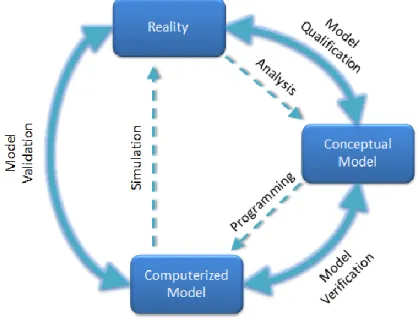
Modeling is the process of producing, verifying, validating, using and comparing models. The diagram presented in Figure 19, first presented in 1979 by the Society for Computer Simulation, shows the primary phases and activities of computer modeling [SCHLESINGER, 1979].
![Figure 47. The result of 64000 points randomly evaluation over the values of (a) x1 and (b) x2 in the range of [-0.5, 0.5] and the 10 bin averages](https://thumb-eu.123doks.com/thumbv2/123doknet/12874887.369590/94.892.172.766.183.361/figure-result-points-randomly-evaluation-values-range-averages.webp)
