HAL Id: hal-01550443
https://hal-univ-paris.archives-ouvertes.fr/hal-01550443
Submitted on 29 Jun 2017
HAL is a multi-disciplinary open access
archive for the deposit and dissemination of
sci-entific research documents, whether they are
pub-lished or not. The documents may come from
teaching and research institutions in France or
abroad, or from public or private research centers.
L’archive ouverte pluridisciplinaire HAL, est
destinée au dépôt et à la diffusion de documents
scientifiques de niveau recherche, publiés ou non,
émanant des établissements d’enseignement et de
recherche français ou étrangers, des laboratoires
publics ou privés.
Comparing plasmonic electrodes prepared by
electron-beam lithography and electrochemical
reduction of an Au (iii) salt: application in active
plasmonic devices
Quynh van Nguyen, Delphine Schaming, Pascal Martin, Jean-Christophe
Lacroix
To cite this version:
Quynh van Nguyen, Delphine Schaming, Pascal Martin, Jean-Christophe Lacroix. Comparing
plas-monic electrodes prepared by electron-beam lithography and electrochemical reduction of an Au (iii)
salt: application in active plasmonic devices. Advances in Natural Sciences : Nanoscience and
Nan-otechnology, IOP Publishing, 2016, 7, pp.015005. �10.1088/2043-6262/7/1/015005�. �hal-01550443�
This content has been downloaded from IOPscience. Please scroll down to see the full text.
Download details:
This content was downloaded by: pascalm IP Address: 81.194.31.219
This content was downloaded on 13/05/2016 at 13:27
Please note that terms and conditions apply.
Comparing plasmonic electrodes prepared by electron-beam lithography and electrochemical
reduction of an Au (iii) salt: application in active plasmonic devices
View the table of contents for this issue, or go to the journal homepage for more 2016 Adv. Nat. Sci: Nanosci. Nanotechnol. 7 015005
(http://iopscience.iop.org/2043-6262/7/1/015005)
Comparing plasmonic electrodes prepared
by electron-beam lithography and
electrochemical reduction of an Au
(
III
) salt:
application in active plasmonic devices
Van-Quynh Nguyen
1,2, Delphine Schaming
1, Pascal Martin
1and
Jean-Christophe Lacroix
11
Université Paris Diderot, Sorbonne Paris Cité, ITODYS, UMR 7086 CNRS, 15 rue Jean-Antoine de Baïf, F-75205 Paris Cedex 13, France
2
University of Science and Technology of Hanoi(USTH), 18 Hoang Quoc Viet, Hanoi, Vietnam E-mail:lacroix@univ-paris-diderot.fr
Received 1 December 2015
Accepted for publication 14 December 2015 Published 27 January 2016
Abstract
This work describes two different methods for obtaining electrodes covered with gold nanoparticles: electron-beam lithography and electroreduction of an Au(III) salt by
chronoamperometry. Localized surface plasmon resonances of these different electrodes have been compared. In a second step, these plasmonic AuNP electrodes were covered with an ultrathin organicfilm of bisthienylbenzene which displays a reversible voltage-dependent switch between conducting and insulating states. The effect of this conductance switch on the plasmonic properties of the AuNPs has been studied.
Keywords: plasmonics, plasmon resonance, nanoparticle Classification numbers: 2.09, 4.02
1. Introduction
Noble metal(gold or silver for instance) nanoparticles (NPs) have been particularly investigated these last decades, due to their remarkable optical and chemical properties. Indeed, they have applications in manyfields, such as optics, electronics, photoelectric devices, catalysis, medicine, sensorsK For some of these applications, it is necessary to immobilize the NPs on solid substrates. Several methods for immobilizing NPs on substrates have been reported. While it is possible to adsorb colloidal NPs by electrostatic interaction [1] or by
using binding molecules[2], it is also possible to obtain NPs
directly on the surface. In particular, a classical method for fabricating substrates with NPs of regular size and controlled
shape is electron-beam (e-beam) lithography [3–7]. Another
classical method relies on vapor-phase gold deposition through a template using polystyrene nanospheres [8–10].
While well-ordered NP arrays can be obtained by these techniques, an easier and cheaper method of making AuNP substrates is the electrochemical reduction of a metal salt, even if this method leads to non-ordered substrates[11,12].
An interesting property of such AuNPs is their localized surface plasmon resonance (LSPR). This phenomenon cor-responds to collective oscillations of the free electrons of NPs, leading at a particular frequency to a resonance phenomenon. This results in a strong optical extinction in the visible or the near-infrared spectral regions. The optical behavior, defined by the resonance wavelength, the bandwidth and the ampl-itude of the LSPR, depends on the metal of the NPs, their size, their shape, and the dielectric constant of the surround-ing medium. Active plasmonic devices, i.e. plasmonic sys-tems for which an external stimulus can reversibly tune the wavelength and/or the amplitude of the LSPR, are the subject |Vietnam Academy of Science and Technology Advances in Natural Sciences: Nanoscience and Nanotechnology Adv. Nat. Sci.: Nanosci. Nanotechnol. 7(2016) 015005 (7pp) doi:10.1088/2043-6262/7/1/015005
Original content from this work may be used under the terms of the Creative Commons Attribution 3.0 licence. Any further distribution of this work must maintain attribution to the author(s) and the title of the work, journal citation and DOI.
of important research efforts. The easiest way to obtain such active plasmonic devices consists in surrounding NPs with switchable materials whose effective dielectric constant is changed by an external input. Several external stimuli have already been employed, based on thermo-[13–15], pH- [16],
photo- [17, 18], electrical- [19] and redox-responsive [3– 7, 20–24] materials, these stimuli allowing to change the
phase[13,14,17–19], the spin [15] or the conductivity [3– 7,21,23,24] of the material. In particular, electrochemically
driven active plasmonic devices have been studied by using conducting polymers as the surrounding media: polyaniline (PANI) [3–5, 21, 23], poly(3,4-ethylenedioxythiophene)
[6,23] or polythiophene [7] and bisthienyl-based oligomers
covalently attached to electrodes via a benzene spacer[7,24].
Indeed, conducting polymers and oligomers can reversibly switch from a reduced insulating state to an oxidized con-ducting state depending on their doping level[25], leading to
a change in their dielectric constant[26,27]. The effect on the
LSPR depends on the size and the shape of the NPs, and on the nature and the thickness of the conducting polymer film deposited on them. The LSPR can be either shifted or damped, depending on the system investigated.
In this paper, two main goals will be addressed. Firstly, we describe a simple new method for obtaining gold NPs by electrochemistry and compare these AuNP substrates with those obtained by e-beam lithography. In particular, their localized surface plasmon resonance (LSPR) has been investigated. Secondly, these plasmonic substrates have been used to generate active plasmonic devices by covering the AuNPs with an ultrathin organic film of bisthienylbenzene (BTB). The effect of the conductance switch of this electro-active organic layer on the properties of AuNPs is reported.
2. Experimental 2.1. Chemical reagents
All chemical products were purchased from Sigma-Aldrich and used without further purification. Indium tin oxide (ITO)-coated glass plates with a resistance of 30–50 Ω/square were purchased from Solems.
2.2. Materials
A CHI 440A electrochemical workstation (CH instruments) was employed in all electrochemical experiments, which were carried out with a conventional one-compartment three-elec-trode cell. A Zeiss Supra 40 scanning electron microscope was used to evaluate the shape and size of AuNPs. The LSPR of AuNPs was recorded using an Ocean Optics HR4000 UV-visible spectrophotometer.
2.3. Electron beam lithography
AuNPs arrays were obtained by electron beam lithography (EBL) performed with a Zeiss Supra 40 scanning electronic microscope (SEM) equipped with a lithographic system (NPGS software). In a first step, a 180 nm thick
polymethyl-methacrylate(PMMA in chlorobenzene, from AllResist) layer was spin coated onto freshly cleaned ITO (with acetone, ethanol and propan-2-ol) and baked at 180 °C to evaporate the solvent. Then, the substrates were exposed to the electron beam, with a typical dose of 370μC cm−2. After exposure, chemical development was performed using methylisobu-tylketone: propan-2-ol (1:3) and then pure propan-2-ol was used to stop the development. Then, a 50 nm thick layer of gold was deposited by an ultravacuum evaporation process (Plassys MEB550S) with an evaporation rate of approxi-mately 0.05 nm s−1. Finally, a lift-off process was performed using acetone in order to remove the remaining PMMA layer together with the gold layer on top whereas, in the areas exposed to the electron beam, the AuNPs resting directly on the ITO substrate remained. The total size of the gratings produced by EBL was limited to 100μm squares.
2.4. Electrodeposition of gold NPs
ITO electrodes were cleaned by sonication for 20 min in dilute alkaline Extran®solution(Merck), then carefully rinsed with distilled water and then ethanol; they were stored in ultrapure milli-Q water (18.2 MΩ cm−1) until required for AuNP electrodeposition. Electrodeposition experiments were carried out by the chronoamperometry technique in a stirred aqueous solution of 2.10−3M KAuCl4and 0.25 M Na2CO3.
The reference was a saturated calomel electrode (SCE) and the counter-electrode was a stainless steel grid. The solution was maintained under argon atmosphere during the whole experiment. AuNPs were deposited on ITO electrodes at a constant potential and a controlled total charge current density.
2.5. BTB grafting
1-(2-Bisthienyl)-4-aminobenzene (BTAB) was synthesized as previously described [28]. Grafting onto substrates was
per-formed using in situ diazonium salt formation: under argon 30 eq. of tert-butyl nitrite were added to a 0.5 mM solution of BTAB in acetonitrile containing 0.1 M of tetra-n-buty-lammonium tetrafluoroborate (TBABF4). BTB was grafted by
multi-scan cyclic voltammetry(CV) (15 successive cycles) in the cathodic range(between 0.3 and −0.5 V/SCE) at a scan rate of 100 mV s−1. By this means,films less than 15 nm thick are generated. A full description of the measurement of the thickness of BTB on gold gratings generated by e-beam can be found in a previous publication [7].
2.6. Localized surface plasmon resonance(LSPR) measurements under electrochemical control
To make LSPR measurements under electrochemical control, a home-made planar three-electrode cell with a stainless steel grid counter-electrode and a silver (Ag/AgCl) pseudo-refer-ence electrode was used. The AuNP array-modified working electrode was placed horizontally on the bottom. The cell was then filled with the electrolyte solution. Absorption mea-surements were carried out with an Ocean Optics HR 4000 UV–visible spectrophotometer coupled with a fiber-optic
2
system which made it possible to analyze an area of 80μm×80 μm. Modulation of LSPR signals was checked by switching the applied potential between a cathodic and an anodic value, either by chronoamperometry or by CV.
3. Results and discussion
3.1. AuNP arrays obtained by e-beam lithography
A classical route to AuNP substrates consists in using e-beam lithography. This method relies on the formation of a nano-hole-based template in a resin, drawn by the electron beam of a scanning electron microscope(SEM), followed by evapor-ating gold into the holes. After a lift-off step allowing to remove the resin, an AuNP array appears on the substrate. The process is explained in more detail in the experimental part of this paper.
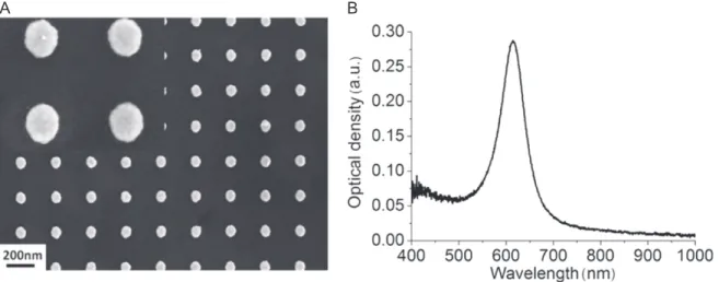
Figure1(A) shows the SEM image of a typical AuNP
array obtained by this technique andfigure1(B) depicts the
corresponding spectrum. The extinction band is attributed to the localized surface plasmon resonance (LSPR) of the AuNPs. The peak is very sharp, with its full-width at half-maximum (FWHM) around 70 nm, which indicates the homogeneity in size of the AuNPs.
The advantage of this technique is not only the possibility of obtaining very perfect AuNP arrays (every NP with the same size, a controlled distance between them, etcK), but also that of modulating the shape and size of the NPs, as well as the distance between them, at will. Nevertheless, this method is a multi-step process which requires not only a long time but also expensive apparatus (electron microscope and metal evaporation apparatus). Moreover, no large-area plas-monic substrates can be obtained by this technique (AuNP arrays are typically around 100μm wide using e-beam lithography).
In this context, there is a strong need to develop low-cost methods to obtain large-area AuNP plasmonic substrates, with good LSPR characteristics.
3.2. AuNP substrates obtained by electrochemistry
We propose an alternative method to obtain AuNP substrates based on the electrochemical reduction of a gold Au(III) salt.
Electrodeposition of AuNP is performed using a chron-oamperometric method from an aqueous KAuCl4 solution
(2 mM) containing Na2CO3 (0.25 M) as supporting
electro-lyte. After the electrochemical process, the ITO electrodes are red or blue, depending on the experimental conditions used, which is clear evidence for the deposition of gold at the nanoscale.
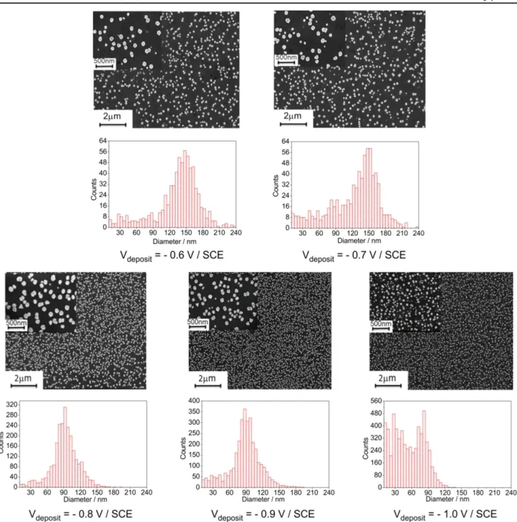
The influence of the potential value applied for gold deposition on the size and dispersity of the AuNPs has been investigated. Indeed, chronoamperometry was performed at various potentials, the total charge density used during the reduction process being fixed at 20 mC cm−2. SEM images (figure2) show that the size of the AuNPs decreases and their
density increases when the electrodeposition potential becomes more negative. This is confirmed by the NP diameter distribution histograms constructed from these SEM images. Indeed, the average size of the AuNPs decreases from 150 nm to 90 nm when the reduction potential decreases from−0.6 V to−1.0 V/SCE. Similar analysis performed on various areas of the sample show no significant variation in the size of the AuNPs, which indicates that their deposition is quite uniform over the 2 cm2area of the ITO electrode.
Figure3shows the optical extinction spectra of the five AuNP substrates corresponding to the SEM images of figure 2, i.e. obtained at different reduction potentials (between −0.6 and −1.0 V/SCE) in fixing the total charge density at 20 mC cm−2. For all samples, the strong absorption in the visible range can be attributed to the LSPR of AuNPs. Spectra taken in various areas of the sample do not show significant variation of the LSPR, confirming that AuNPs are uniformly deposited on the ITO electrode. The LSPR max-imum wavelength is blue-shifted from 680 nm to 580 nm when the applied potential goes from −0.6 to −1 V/SCE, which is consistent with the formation of smaller AuNPs when it becomes more negative. Moreover, the full width at half maximum(FWHM) of the LSPR decreases from 200 to
Figure 1.(A) SEM image of an AuNP array obtained onto ITO using e-beam lithography method (oblate particles, 80 nm in diameter, 50 nm
high and 250 nm gratings), (B) optical extinction spectrum corresponding to this arrays.
3
80 nm on going from −0.6 to −1 V/SCE, showing an improvement in the optical response of the substrates. In particular, the sharpness of the LSPR signals observed for reduction potentials between −0.8 and −1 V/SCE is char-acteristic of plasmonic substrates with high quality factor, the FWHM being comparable to that of substrates obtained by e-beam lithography.
In these experiments, it appears that the potential used to reduce the gold salt has a marked influence on AuNP nuclea-tion. Indeed, the higher the negative potential, the easier nucleation will be, leading to an increase in the number of nuclei and in the overall NP density. As the total charge density used during electroreduction was kept constant for each
deposition, a high density manifests itself in the formation of smaller NPs (at high negative potentials) while a low density leads to larger NPs(at low negative potentials). A more detailed explanation concerning the processes involved during the electrosynthesis of AuNPs has been recently published[24].
3.3. Electroactive plasmonic devices
3.3.1. BTB electrografting onto AuNP electrodes. These two kinds of AuNP substrates have been compared for use as plasmonic electrodes in electroactive plasmonic devices.
An ultrathin organicfilm of oligoBTB was deposited on each kind of electrode by electroreduction of the
Figure 2.SEM images of AuNPs electrodeposited onto ITO at various reduction potentials(−0.6 to −1.0 V/SCE and fixed total charge density(Q=20 mC cm−2), and corresponding AuNP diameter distribution histograms.
4
corresponding diazonium salt [28]. The resulting covalently
bonded layer is less than 15 nm thick[7]. Such a molecular
film is known to undergo a reversible conductance change with variation of the voltage [28, 29], switching between a
totally blocking reduced state and a conducting oxidized state at close to 0.6 V/SCE. Such a conductance switch can induce a change in the dielectric constant of the BTB layer and affect the LSPR signal.
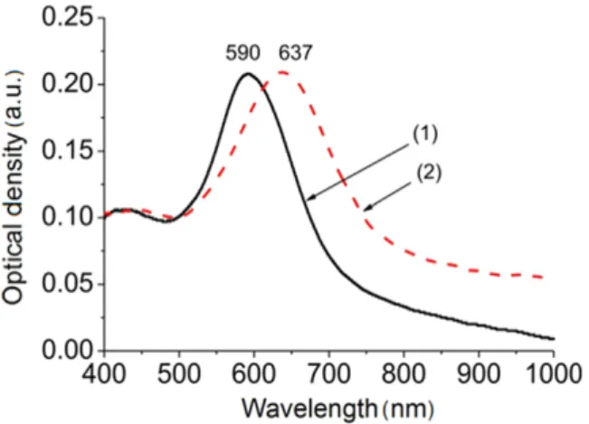
After BTB had been grafted onto the AuNP substrates, a red-shift of the LSPR was observed(figure4), whatever the
process used to perform AuNP substrates. This red-shift of 40–70 nm is attributed to the modification of the dielectric environment [30–32] induced by the deposition of the thin
film. Such a red-shift is commonly observed when the dielectric constant of the medium surrounding the NPs increases[7,30–32].
3.3.2. Electrochemical polarization of BTB|AuNP|ITO electrodes. The effect of the BTB conductance switch on the LSPR of AuNPs was investigated by varying the
polarization of the BTB|AuNP electrodes. Ferrocene (Fc) was added to the electrolyte solution in order to ensure the stability of the BTB layer, since BTB is oxidized to reactive radical-cations. Indeed, under these conditions, BTB acts as a molecular bridge to oxidize Fc in solution and, thus, the accumulation of charges in the BTB film and solid-state coupling between reactive BTB radical cations, leading to film degradation, are avoided.
Figures 5(A) and (B) display the optical extinction
spectra of BTB|AuNP devices obtained by e-beam lithogra-phy and electrodeposition, respectively, during the electro-chemical switch from the reduced state to the oxidized state of BTB. Similar effects are observed whatever the BTB|AuNP electrode used. Indeed, a broadening accompanied by a decrease in the intensity of the LSPR band is observed, clearly showing modulation of the LSPR by the switching of the thin layer of BTB. Nevertheless, no shift of the LSPR band is observed. These dampings are large compared to previously reported equivalent systems. Indeed, while marked dampings are observed when thick layers (for example, a layer of a conducting polymer such as a PANI film) are deposited on AuNPs[5], the effects are generally smaller for
NP systems using ultrathin films or molecular monolayers [22]. The quite large damping observed in our case can be
attributed to the covalent bonds between the BTB and the AuNPs[7].
Such observations can be qualitatively explained by the Drude free-electron model [33–35], in which the dielectric
function of a conductive material is complex (ε=εRe+iεIm) while the dielectric function of an insulating
material is described only by a real value. In our case, the observed damping of the LSPR band, when the BTB layer shifts from its reduced state to its oxidized state, indicates that the imaginary part of the dielectric constant(εIm) of the BTB
increases sharply, which is in agreement with a switch of the BTB film between an insulating and a conducting state [7,26,27]. This damping can be attributed to charge transfer
between plasmon-generated hot electrons and the BTBfilm in its conducting state, which acts as an efficient acceptor, the LSPR lifetime being decreased by the presence of an additional decay channel[36]. On the other hand, the absence
of LSPR band shift when the BTBfilm is switched indicates that the real part of the dielectric constant (εRe) of the film
does not change significantly [7,26,27].
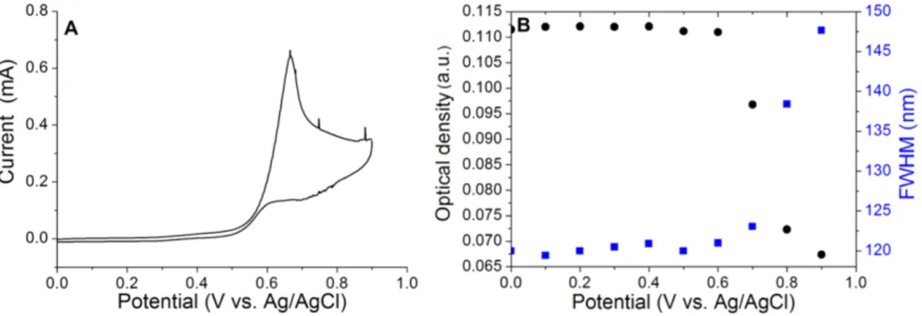
A more detailed study can be performed by scanning the potential by CV. Figure 6 shows how the intensity at the LSPR maximum and its FWHM depend on the potential applied during the CV, in the case of a BTB|AuNP electrode obtained by electrodeposition. In the forward scan, as long as the BTB film remains in its blocking state, i.e. when the potential is below 0.6 V/SCE, no or very little LSPR modulation occurs. However, when charges are injected into the BTBfilm, leading to its conductive state, the LSPR signal is progressively damped. Note also that the initial LSPR signal was restored upon polarization of thefilm at 0 V.
Figure 3.Optical extinction spectra of AuNPs on ITO electrodes obtained at various reduction potentials(−0.6 V (curve 1), −0.7 V (curve 2), −0.8 V (curve 3), −0.9 V (curve 4) and −1 V/SCE (curve 5)) and with a total charge density, Q=20 mC cm−2.
Figure 4.Optical extinction spectra of an AuNP electrode obtained by electrodeposition(−0.8 V/SCE and 20 mC cm2), before (curve 1) and after (curve 2) BTB deposition.
5
4. Conclusions
In this work we have compared electroactive plasmonic devices using AuNP|ITO electrodes obtained in two different ways: e-beam lithography and electroreduction of an AuIII
salt by chronoamperometry. The first method (e-beam litho-graphy) leads to very well ordered AuNP arrays. Never-theless, this technique is a multi-step process with requires not only a long time but also expensive apparatus (electron microscope and metal evaporation apparatus). Moreover, it allows to generate only very small AuNP arrays, typically around 100μm wide. On the contrary, the second method (electroreduction of a gold salt) is a low-cost technique allowing the formation of large-area AuNP plasmonic sub-strates. Despite the lack of organization of the NPs, the AuNP substrates produced by this method have an optical response close to that of the samples fabricated by e-beam deposition. Moreover, AuNP substrates are obtained by electrochemistry on electrodes of several square centimeters in area in less than 100 s in a one-step template-free process.
In a second step, these plasmonic AuNP electrodes were covered with an ultrathin organicfilm of BTB which displays a reversible voltage-dependent switch between a conducting and
an insulating state. The effect of this conductance switch on the plasmonic properties of the AuNPs was studied, and the results were the same whatever the method of preparation of the AuNP substrate. When thefilm is switched from its insulating state to its conducting state, a marked damping of the LSPR band, with a large intensity decrease and a strong FWHM increase, is observed. These observations indicate that the LSPR lifetime of AuNPs is smaller when BTB is in its con-ducting state. These changes are probably due to charge transfer between plasmon-generated hot electrons and the conducting BTB, which acts as an efficient electron acceptor. It is remarkable that this large LSPR modulation is obtained with a film which is less than 12 nm thick. These results are important to academic investigations of nanoscale materials. In view of the increasing demand for ultimate miniaturization of electronic and photonic systems, applications of active plas-monic devices as sensors or routers can be foreseen.
Acknowledgments
This work was supported by the CNRS (France), the Uni-versity Paris Diderot(Paris, France) and by a PhD grant from
Figure 5.Optical extinction spectra AuNP electrodes obtained by(A) e-beam lithography and (B) electrodeposition, and overcoated with an 8–12 nm BTB film in its reduced state (0.2 V/SCE, red dashed line) and in its oxidized state (0.9 V/SCE, blue full line).
Figure 6.(A) CV of Fc (1 mM) in 1 M LiClO4solution in acetonitrile on a BTB|AuNP electrode obtained by gold electroreduction (scan rate:
100 mV s−1) and (B) variation of the LSPR band intensity maximum and FWHM of this band during one CV scan.
6
the University of Science and Technology of Hanoi (Vietnam).
References
[1] Gole A, Orendorff C J and Murphy C J 2004 Langmuir
20 7117
[2] Brust M, Bethell D, Kiely C J and Schiffrin D J 1998 Langmuir
14 5425
[3] Leroux Y R, Lacroix J C, Chane-Ching K I, Fave C, Félidj N, Lévi G, Aubard J, Krenn J R and Hohenau A 2005 J. Am. Chem. Soc.127 16022
[4] Leroux Y, Lacroix J C, Fave C, Trippé G, Félidj N, Aubard J, Hohenau A and Krenn J R 2008 ACS Nano2 728 [5] Leroux Y, Lacroix J C, Fave C, Stockhausen V, Félidj N,
Grand J, Hohenau A and Krenn J R 2009 Nano Lett.9
2144
[6] Stockhausen V, Martin P, Ghilane J, Leroux Y,
Randriamahazaka H, Grand J, Félidj N and Lacroix J C 2010 J. Am. Chem. Soc.132 10224
[7] Schaming D, Nguyen V Q, Martin P and Lacroix J C 2014 J. Phys. Chem. C118 25158
[8] Hulteen J C and Van Duyne R P 1995 J. Vac. Sci. Technol. A
13 1553
[9] Ye X and Qi L 2011 Nano Today6 608
[10] Hulteen J C, Treichel D A, Smith M T, Duval M L, Jensen T R and Van Duyne R P 1999 J. Phys. Chem. B
103 3854
[11] Sakai N, Fujiwara Y, Arai M, Yu K and Tatsuma T 2009 J. Electroanal. Chem.628 7
[12] Fernàndez-Blanco C, Colina A, Heras A, Ruiz V and Lopez-Palacios J 2012 Electrochem. Commun.18 8 [13] Karg M, Pastoriza-Santos I, Pérez-Juste J, Hellweg T and
Liz-Marzan L M 2007 Small3 1222
[14] Gehan H, Mangeney C, Aubard J, Lévi G, Hohenau A, Krenn J R, Lacaze E and Félidj N 2011 J. Phys. Chem. Lett.
2 926
[15] Abdul-Kader K et al 2013 Nanoscale5 5288
[16] Pita M, Krämer M, Zhou J, Poghossian A, Schöning M J, Fernandez V M and Katz E 2008 ACS Nano2 2160
[17] Sidhaye D S, Kashyap S, Sastry M, Hotha S and Prasad B L V 2005 Langmuir21 7979
[18] Hira T, Homma T, Uchiyama T, Kuwamura K and Saiki T 2013 Appl. Phys. Lett.103 241101
[19] Khatua S, Chang W S, Swanglap P, Olson J and Link S 2011 Nano Lett.11 3797
[20] Wang Z and Chumanov G 2003 Adv. Mater.15 1285
[21] Leroux Y, Eang E, Fave C, Trippé G and Lacroix J C 2007 Electrochem. Commun.9 1258
[22] Zheng Y B, Yang Y W, Jensen L, Fang L, Juluri B K, Flood A H, Weiss P S, Stoddart J F and Huang T J 2009 Nano Lett.9 819
[23] Baba A, Tada K, Janmanee R, Sriwichai S, Shinbo K, Kato K, Kaneko F and Phanichphant S 2012 Adv. Funct. Mater.
22 4383
[24] Nguyen V Q, Schaming D, Martin P and Lacroix J C 2015 Electrochim. Acta179 282
[25] Inzelt G 2008 Conducting Polymers—A New Area in Electrochemistry ed F Scholtz(Berlin: Springer)
[26] Baba A, Lübben J, Tamada K and Knoll W 2003 Langmuir
19 9058
[27] Baba A, Tian S, Stefani F, Xia C, Wang Z, Advincula R C, Johannsmann D and Knoll W 2004 J. Electroanal. Chem.
562 95
[28] Fave C, Leroux Y, Trippé G, Randriamahazaka H, Noel V and Lacroix J C 2007 J. Am. Chem. Soc.129 1890
[29] Stockhausen V, Ghilane J, Martin P, Trippe-Allard G, Randriamahazaka H and Lacroix J C 2009 J. Am. Chem. Soc.131 14920
[30] Jensen T R, Duval M L, Kelly K L, Lazarides A A, Schatz G C and Van Duyne R P 1999 J. Phys. Chem. B
103 9846
[31] Kelly K L, Coronado E, Zhao L L and Schatz G C 2003 J. Phys. Chem. B107 668
[32] Miller M M and Lazarides A A 2005 J. Phys. Chem. B109 21556
[33] Kohlman R S, Joo J, Min Y G, MacDiarmid A G and Epstein A J 1996 Phys. Rev. Lett.77 2766
[34] Prigodin V N and Epstein A J 2002 Synthetic Met.125 43
[35] Tzamalis G, Zaidi N A, Homes C C and Monkman A P 2002 Phys. Rev. B66 085202
[36] Hoggard A, Wang L Y, Ma L, Fang Y, You G, Olson J, Liu Z, Chang W S, Ajayan P M and Link S 2013 ACS Nano7 11209
7