HAL Id: hal-01005317
https://hal.inria.fr/hal-01005317
Submitted on 12 Jun 2014
HAL is a multi-disciplinary open access
archive for the deposit and dissemination of
sci-entific research documents, whether they are
pub-lished or not. The documents may come from
teaching and research institutions in France or
abroad, or from public or private research centers.
L’archive ouverte pluridisciplinaire HAL, est
destinée au dépôt et à la diffusion de documents
scientifiques de niveau recherche, publiés ou non,
émanant des établissements d’enseignement et de
recherche français ou étrangers, des laboratoires
publics ou privés.
FPGA-based Implementation of Multiple PHY Layers of
IEEE 802.15.4 Targeting SDR Platform
Albdelbassat Massouri, Tanguy Risset
To cite this version:
Albdelbassat Massouri, Tanguy Risset. FPGA-based Implementation of Multiple PHY Layers of IEEE
802.15.4 Targeting SDR Platform. SDR-WInnComm, Apr 2014, Schaumburg, Illinois, United States.
�hal-01005317�
FPGA-based Implementation of Multiple
PHY Layers of IEEE 802.15.4
Targeting SDR Platform
Abdelbassat MASSOURI and Tanguy RISSET
Universit´e de Lyon, INRIA,
INSA-Lyon, CITI-INRIA, F-69621, Villeurbanne, France
[email protected]
Abstract—While SDR platforms become more and more accessible to a large community of researchers with affordable prices, open source FPGA-based implementation of wireless communication systems are still not available. This paper presents an open source FPGA-based design of IEEE 802.15.4 PHY Layers developed in the context of a new SDR testbed named FIT/CorteXlab. We propose a VHDL implementation of the three available options of the IEEE 802.15.4 physical layer parametrized and easily reconfigurable. We have validated our design on Nutaq platform which combines Xilinx Virtex-6 FPGA and tunable Radio420x RF transceiver. A tutorial style approach is adopted to describe the multiple PHY Layers of both the baseband TX and RX IPs of IEEE 802.15.4 standard. More focus is given to the symbol timing/carrier recovery and considerations for FPGA implementation are outlined. The IPs presented here will participate to the building of an open source hardware SDR library similar to GNU radio but targeted to FPGA-based platforms.
Keywords—IEEE 802.15.4, Zigbee, Software Defined Radio, Cognitive Radio, FPGA.
I. INTRODUCTION
Software Defined Radio (SDR) has been identified by Mitola many years ago [8], but the SDRtechnology has been accessible at reasonable price only recently. Based on this technological shift, the advent cognitive radio networks is a major research challenge as it has been pointed by NSF
in 2009 [16]. One of the recommendations of this report concerned the lack of cognitive radio testbeds and the urge to “develop a set of cognitive networking test-beds that can
be used to evaluate cognitive networks at various stages of their development”.
While open source software is widely used for cooperative academic project, open source hardware is still hard to find. OpenCores [13] is one of the most well known organization providing open sourceVHDL, but it mainly provides processors because it does not target a particular application domain. Providing dedicated IPs for a particular application domain, here SDR, will help in building a common source repository. An example of such closed community is the reconfigurable
video coding standard framework [7] supported by MPEG to help in developping portable video coding applications. Given that cognitive radio is foreseen as a major innovative field in the next ten years, it will need a similar effort to help new waveform deployement on various SDR architectures.
However, modern wireless technologies based on OFDM
(Orthongonal Frequency Division Multiplexing) such as WiFi or LTE-Advanced suffer from a major disavantage: they re-quire a high computing power. For instance, LTE-Advanced is suppose to require 40Gops with a power consumption of less than 1 Watt. Hence, dedicated hardware IPs have to be used to meet the computing power required. This explains the fact that no open-source library exists so far for this domain: dedicated
IPs are very specific to their target protocol and moreover their design is very time-consuming. This situation should change as it will become mandatory to provide re-usable code for software defined radio as the technology is mature now. The growing use of software radio application will improve the development of open source hardware design for digital signal processing and we contribute, with the design presented here, to this developpement
In section II, we briefly review existing testbed that can be used for SDR application and we present the FIT/CorteXlab testbed. Section III presents the multiple PHY layers that we provide according to the IEEE 802.15.4 standard. Finally, the performance of the implementation of our design on Virtex 6
FPGAis presented.
II. SDR TESTBED
Recently, many testbeds have been built in the field of wireless communications, targeted to wireless sensor or Wifi networks. However, only a few large-scale testbeds have been developed in the SDR and cognitive radio field (CREW [15],
TRIAL andCORNET[11] are the main ones).
We are currently building a new cognitive radio testbed in Lyon named CorteXlab (see figure 1), as part of the Future Internet of Things [4] french funding. Cognitive radio nodes together with wireless sensor nodes will be deployed in a electromagnetically isolated room so as to bring radio propa-gation under control. The testbed will be open to the scientific community within two years and will allow academics and industrials to conduct real-life cognitive radio experiments. Nodes will be remotely programmable just as if users had them on their desk.
In [3], a survey of existing SDR architectures highlights the fact that there is currently no accepted common execution model for SDR platform. However, we believe that the use
Electromagnetically isolated room Internet CR node WS node CR node spectrum analyzer spectrum generator ... ... ... ... ... ... ... ... ... ... ... user user CR : cognitive radio WS : wireless sensor
Fig. 1: Hardware/software requirements for the CorteXlab cognitive radio node (figure from [3]).
is currently the most promising approach for prototypes. In CorteXlab, two types of nodes have been deployed: USRP
nodes from National Instrument [10] and picoSDRnodes from Nutaq [12]. In this paper, we target the programming of picoSDR nodes, but the IPs designed should be portable to other platforms using FPGA, except for the IP implementing the interface between theFPGAand the rest of the board which is usually provided by the board supplier.
One objective of the CorteXlab testbed is to propose open source reference designs as a support for remote experimenta-tion. Particularly it aims at providing :
• Tunable single carrier reference design. We have cho-sen the Zigbee (802.15.4) standard as defined byIEEE
[6]. This is the main contribution of this paper. • Tunable multiple carrier reference design :SISO/OFDM
and MIMO/OFDM which are not presented in this paper.
The software architecture and the room have been selected to target reproducibility and control over the radio propagation and the nodes will have the computing power to runWiFi/LTE
in real-time at standard rates and using 2x2 MIMO. The room will contain 22 USRP nodes programmed with GNU radio, 12 2x2MIMOand 6 4x4MIMOpicoSDRnodes fully integrated and based on a powerful FPGA. Fig. 2 presents the current status of the room: electromagnetic isolation has been performed.
The generic SDR execution model that we target is
illus-trated on Fig. 3. From our experience, mostSDRplatform using aFPGA propose a radio control mechanism based onSPIbus, and provide a soft core on the FPGA to handle it. However, it is mandatory to have a direct pipelined data path from the board to the RF front-end in order to take advantage of the maximum throughput available for signal processing data.
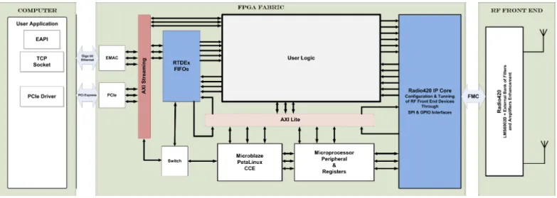
Fig. 4 shows the generic architecture of application de-ployed on Nutaq family of board. The picoSDRuses a similar architecture for PHY layer implementation. Each picoSDR
board includes one or two Perseus 6011 advanced mezzanine card, each of which contains a Virtex-6 FPGA connected to two Radio420x RF front-end. The Perseus board contains a Virtex6 FPGA connected on one side to a host processor handling the MAC and application layers and on the other side to the Radio420x front-end. The platform is provided with
Fig. 2: Current status of FIT/CortexLab room, SDRpltaform will be attached to the roof, the room will has now 50 dB
isolation so as to provide reproducible experimental environment.
Fig. 3: Targeted SDR platform architecture model, including an FPGAcontaining a high bandwidth datapath between the CPU and the RF front-end where ourIP can be insterted
a reference design that includes a MicroBlaze softCore used for configuration of the radio front-end and a high speed bus named RTDEx (for Real Time Data Exchange). In fact, the key to efficient SDR application is the efficient handling of the data flow between the front-end and the host processor. the core of the baseband processing is performed in the User
logic IP of Fig. 4, one can see that it is a particular instance of the generic model that we have drawn in Fig. 3. Therefore, the main objective of the Nutaq RTDEx IP core is to provide
a framework to exchange data with a host device through the GbE or PCIe links with the highest bandwidth and lower latency possible. In order to avoid any bottleneck in the data throughput, the MicroBlaze processor is bypassed during data packet transmission allowing the full data bandwidth and lower latency due to AXI bus enhanced features compared to the PLB one.
The picoSDR RF front-end is an FPGA Mezzanine Card (FMC) named Radio420X. It is a powerful multimode SDR RF transceiver module designed around the state-of-the-art, multistandard, multiband Lime Microsystems LMS6002D RF transceiver IC. The LMS6002D bandwidth, which is selectable on-the-fly, makes it suitable for a large number of narrowband and broadband applications with excellent channel selectivity. In addition to the integrated analog filters and amplifiers of the LMS6002D RF transceiver, the front end RF card includes external bank of filters and amplifiers that allow better performance.
Fig. 4: Nutaq Board Support Development Kit for SDR platforms.
picoSDR platform allows using three design flows: BSDK
(Board Support Design Kit),MBDK(Model Based Design Kit) and GNUradio design flow. BSDK is the design flow adopted in the context of CorteXlab testbed to enable HDL design and implementation of open source IPs for SDRsystems. The
open quality refers to the VHDL code we have developped, Nutaq’s and Xilinx’s IPs provided with the platform (RTDEx bus, EMAC, PCIe, Radio420 Core, etc) are free of charge but not open source of course. The Nutaq Board Software Development Kit (BSDK) is a complete set of tools that includesIPcores, Frameworks,APIs as depicted on the Fig. 4. On top of industry standard board level libraries andAPIs, the
BSDK includes a complete and efficient transport layer (CCE: Central Communication Engine) that both allows remote con-trol and high speed data exchange between NutaqFPGA-based
hardware and standard processor blades or remote computer. A typical picoSDR-based design include a MicroBlaze pro-cessor instantiated within the FPGAfabric running a commer-cial embedded Linux distribution named Petalinux. This fabric risk processor runs Nutaq CCE application and may also run user-defined task/application. TheCCEhandles the bootloader, the start-up sequence, theTCP-IPandPCIe communication and configuration commands, etc. This software component is the board interface with the host Command Line Interpreter, GUIs
or any other software running on a remote computer intended to communicate with the Nutaq FPGA-based hardware.
Figure 5 shows the testbed we used for design, implementa-tion, test and validation of theSDRopen sourceIPs. It consists of two picoSDRnodes: the first is a 4x4 node and the second is a 2x2 with an embedded computer. For instance a windows computer is used forHDLcoding and synthesizing and another computer with Debian operating system is used for software development of C applications based on Nutaq EAPI.
III. MULTIPLEPHY LAYERSDESIGN& IMPLEMENTATION
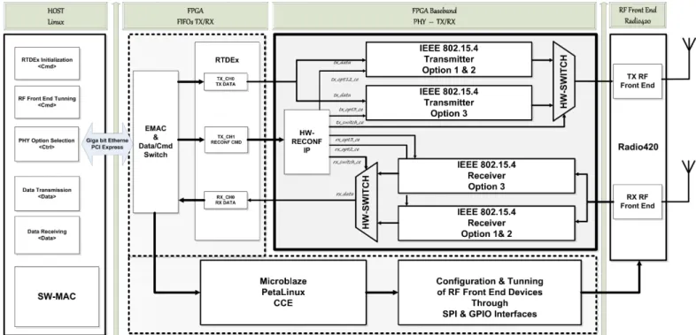
This part specifies the hardware TX and RX architectures of IEEE 802.15.4 PHY layers that we have implemented. The
complete hardware design has been represented in Fig. 6.
Fig. 5: Development testbed : 2 PicoSDRs and Host machines.
IEEE 802.15.4 standard proposes three options to implement a compliant transmitter [6]. Such a compliant device shall operate in one or several frequency bands using the modulation and spreading formats summarized in Table I. For this, the
IP designed should be reconfigurable to adapt to the different parameters (chip rate, frequency band, etc.).
Although IEEE 802.15.4 standard is intended to conform with established regulations in Europe, Japan, Canada, and the United States, CorteXlab testbed is shielded and electromag-netically isolated environment that allows users to experiment all the options regardless of regulatory constraints. One can even transmit and receive at any frequency in the range of 0.3 - 3.8 GHz. Thus, this unique feature will help to extend the experimentation use cases and enable exploration of further opportunities to enhance wireless communication technologies. Naturally according to Table I, option 1 and option 2 physical layer specifications are slightly the same except the chip and the symbol rates. For this reason they are represented by the same IP which can be configured to run in mode 1 or mode 2 by simply changing the input clock. The latter is performed through a software reconfiguration that easily
Fig. 6: Block diagram of our multiple PHY layers implementation of the IEEE 802.15.4 standard.
TABLE I: IEEE 80.15.4 PHY Layer Specifications.
PHY Option Frequency Band (MHz)
Spreading Parameters Modulation Data Parameters Filter Parameters Chip rate (kcps) Spreading Sequence Length Number of Sequence Bit rate (kbps) Symbol rate (kips) Symbols
Option 1 868-868.6 300 16 2 BPSK 20 20 Binary Raised
Cosine Filter
Option 2 902-928 600 16 2 BPSK 40 40 Binary Raised
Cosine Filter Option 3 2400-2483.5 2000 32 16 O-QPSK 250 62.5 16-ary
Orthogonal
Half-Sine Filter
modify the design clock provided by the PLL of the Radio420x transceiver. Hence, we greatly minimize the FPGA resources needed to map this multiple mode design.
Nevertheless, option 3 physical layer specifications are extremely different from those of option 1 and option 2. Furthermore, option 3 physical layer specifications are more complex to design and implement in hardware. Hence it is natural to provide a hardware switch IP to switch between option 1/2 and option 3 IPs as illustrated in Fig. 6. The basebandIP(shaded on Fig. 6) is plugged to a dedicated FIFO
of theRTDEx bus (in the case of implementation on picoSDR) and it communicates with a softwareAPIrunning on the host. The latter sends the user choice (option 1/2 or 3) to the HW switch through Gigabit Ethernet or PCIExpress link to enable
the suitable IP accordingly.
In the same way as the transmitting path of the multiple layers implementation of the IEEE 802.15.4 standard, the re-ceiving path contains two receivers each one of them performs data reception and decoding according to the enabled option. The switching process is controlled by a Finite State Machine that enables one of those receivers and configure the switch to
output the expected stream as illustrated in the Fig. 6. One can see in this figure the software tasks that should be performed on the computer side such asRTDEx initialization,RFfront-end tuning, PHYoption selection, data transmission and reception. Therefore, in parallel to the baseband IPs the FPGA fabric instantiate the Microblaze softCore running the CCE (central communication engine) and other IP cores used to configure the RTDEx bus, to tune and to perform the suitable connection with the RF front-end devices.
In the next subsections, we consider the transmitter and the receiver architectures of the physical layer, first for option 1 and 2, then for option 3.
A. TX Architecture
In this section we present the baseband architecture of the IEEE 802.15.4 transmitters we implemented in this work. The IEEE standard [6] indicates how to form the frame, and the performance that should be obtained by the receiver, but does not specify exactly how the receiver should be implemented. Hence, it is much more open and difficult to implement the receiver part. In particular synchronization mechanism has to
be carefully designed, this is one of the contribution of this paper.
Fig. 7: Block diagram of IEEE 802.15.4 option 2 Transmitter.
1) TX architecture of PHY Layer Option 1 & 2: The data rates of options 1 and 2 are respectively 20 kb/s and 40 kb/s. Both of option 1 and 2 use direct-sequence spread spectrum (DS-SS) with binary phase-shift keying (BPSK) used for chip modulation and differential encoding used for data symbol encoding. Each input bit shall be mapped into a 15-chip pseudo-random sequence as specified in Table II.
TABLE II: IEEE 80.15.4 Option 1& 2 symbol-to-chip mapping.
Input symbol (bits) Chip values c0c1· · · c14
0 111101011001000 1 000010100110111
The block diagram of the TX chain is provided in Fig. 7, it basically corresponds to the corresponding IP implemented. The IEEE 802.15.4 frame arrives splitted in 32 bit word from the RTDEx FIFO bus, each bit is encoded with respect to the previous bit in the differential encodingIP. The symbol to chip
IP multiply the sample rate by 15 using table II. Modulation is performed using BPSK, then upsampling and pulse shaping are performed before digital to analog conversion which is performed in the RF front-end.
Configuration switching between Option 1 and 2 is simply done by reconfiguring the design clock provided by thePLLof the RF front-end. This reconfiguration process uses the Nutaq
API to send a command with the sampling frequency of the
ADCandDACto theCCEthrough the gigabit ethernet link. The
CCE running on the MicroBlaze SoftCore decodes the value of the sampling frequency and uses it to configure the PLL
on the Radio420x through anSPIinterface. This configuration allows the generation of the reference clock of the baseband
IPs which is two times the sampling frequency.
Fig. 8: Block diagram of IEEE 802.15.4 option 3 Transmitter
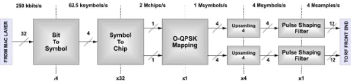
2) TX architecture of PHY Layer Option 3: The spec-ification of the third option of IEEE 802.15.4 PHY layer
supports data rate of up to 250kb/s. It usesDS-SSwithO-QPSK
(offset quadrature phase shift keying) as modulation type. Each O-QPSKsymbol is one of 16 orthogonal pseudo-random sequences. Each symbol is 32 chip long and corresponds to one of 16 possible combinations of four bits as partly depicted in Table III. The resulting chip rate is 2 Mchips/s. Fig. 8 illustrates a typical block diagram of the implemented IP of a transmitter conform to the option 3 specifications.
TABLE III: IEEE 80.15.4 Option 3 symbol-to-chip mapping.
Data symbol Data symbol Chip values (sk)10 (sk)2 c0c1· · · c31 0 0000 11011001110000110101001000101110 1 0001 11101101100111000011010100100010 2 0010 00101110110110011100001101010010 . . . 14 1110 10010110000001110111101110001100 15 1111 11001001011000000111011110111000 B. RX Architecture
As indicated in Fig. 9, a typical digital receiver receives the digitized complex baseband signal from RF front-end transceiver. Then it applies a matched filter in order to max-imize the signal to noise ration (SNR). The received signal contains not only the data symbols that should be decoded but also unknown parameters such as frequency and phase offsets and the sampling time. Therefore, an accurate estimation of these parameters is vital for reliable data detection. The dis-cussion below outlines some possible methods for estimating carrier offset and sampling time. Once the compensation for distortion and timing recovery are performed, the gathered symbols are then processed by a detector. Detection processing can be a very simple device that makes decision of either a symbol is 0 or 1. However, in communication standards data are formatted in a specific way to help easy decoding procedure as it is the case of IEEE 802.15.4 standard. For instance, preamble and start of frame delimiter (SFD) are added to the frame to help symbol time synchronization and enable the data decoding. Thus, the detector module of Fig. 9 must perform complex baseband processing including preamble correlation,
SFDcorrelation, and a bank of symbol correlators to detect the correct symbols as it will be outlined later in this section.
Fig. 9: Block diagram of a coherent receiver.
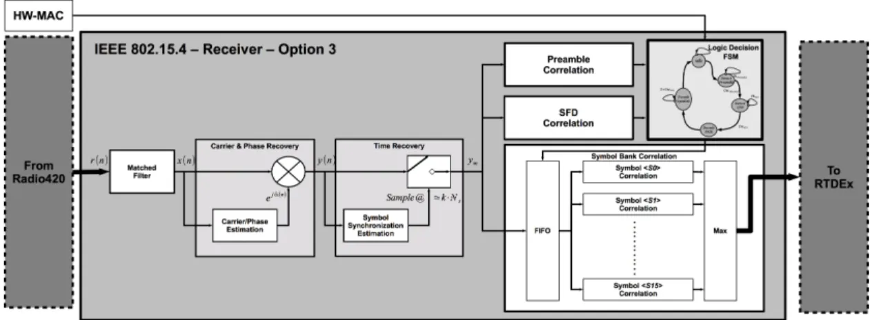
This section will provide a useful and understandable way to implement most of the receiver functionalities such as energy detection, carrier and phase recovery, clock recovery, symbol correlation, preamble correlation, SFD correlation, etc. The receiver is also duplicated for option 1/2 and option 3. In fact, we implemented two receivers one for each option as illustrated inn Fig. 6. Those receivers share the same structure
as illustrated in Fig. 9. However, they are little bit different from an implementation point of view since in the case of option 3 the baseband digital processing is performed on both I and Q signals whereas in the case of option 1/2 BPSK
modulated signal is simple to demodulate. For instance, the major difference between the two receivers is naturally the decoder IPwhere massive correlations are performed to detect the preamble and the SFD in addition to decoding procedure of symbols.
Fig. 10 presents our implementation of option 3. The
detector bloc includes two correlators, one used for preamble detection and the other used for frame delimiter detection, a small controller (FSM for finite state machine), and the symbol bank correlation. The symbol bank correlation is in charge of comparing blocs of 32 chips against data symbol in a bank to recover the coded data symbols (reverse work as the one presented in table III). Before that, the frame has to be synchronized. When the FSM is informed by the preamble correlationIPthat a preamble has been detected, it launches the start frame delimiter detection (SFD correlation). When SFD
is detected, data are send bloc by bloc to the symbol bank correlator.
The rest of the section focus on the implementation of synchronization and correlation functions in the receiver which are the main technical difficulties of this IP.
1) Carrier and Phase Recovery: In a typical wireless communication system, imperfect up-conversion and down-conversion caused by non-ideal transmitter and receiver local oscillators result in a carrier offset at the receiver. This offset causes a continuous rotation of the signal constellation, and must be corrected in order to achieve reliable demodulation of the received signal.
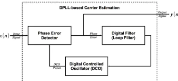
Fig. 11: Basic block diagram of a Digital Phase Locked-Loop (DPLL) used for carrier offset
There are many ways to implement carrier synchronization in a digital communication system. We present here a method that tune together the frequency and phase, hence carrier and phase are simultaneously recovered. At the heart of all synchronizers is the phase-locked loop (PLL). A basic block diagram is shown in Fig. 11. This DPLL consists of three modules : the phase detector, the loop filter and the digital controlled oscillator. It employs proportional and integral loop filters formed by a scaled digital integrator and a scaled direct path. The filter coefficients control the PLL bandwidth and damping factor. In the PLL digital implementation, the DCO
takes the form of a direct digital synthesizer (DDS). The phase detector can be implemented using the arctangent operation which can be performed by a CORDIC IP in vectoring mode
[1].
The schematic view of the DPLL IP we implemented is given in Fig. 12. It contains a phase detector, an error generator and a loop filter. The purpose of the phase detector and DCO
is to detect the phase of the input signal then rotate it by the estimated phase at the output of the loop filter. Therefore, those functions (of the Phase detector and the DCO) can be combined and simply implemented by a CORDIC module in rotation mode as illustrated in Fig. 12. In the next section we will present the functional description of theCORDICalgorithm in rotation mode and we will describe some aspects related to its HDL implementation.
Fig. 12: Block diagram of the implemented second-order
DPLL
a) CORDIC in Rotation Mode: In the rotation mode, the angle accumulator is initialized with the desired rotation angle. The rotation decision at each iteration is made to diminish the magnitude of the residual angle in the angle accumulator. The decision at each iteration is therefore based on the sign of the residual angle after each step. For rotation mode, the CORDICequations are [1] :
xi+1= xi− yi· di· 2−i yi+1= yi− xi· di· 2−i zi+1= zi− di· tan−1(2−i) where
di= −1 if zi<0 , + 1 otherwise
which provide the following result :
xn = An· (x0· cos z0− y0· sin z0) yn = An· (y0· cos z0+ x0· sin z0) zn = 0 An = n Y i=1 p 1 + 2−2i
The CORDIC algorithm can be implemented either in an iterative way or as a pipelined architecture. Iterative CORDIC
implementation takes more than a clock cycle for each output value. It is useful when theFPGAresources are limited and the
Fig. 10: Block diagram of IEEE 802.15.4 option 3 Receiver
design speed is not high. However, pipelined implementation provides an output values each clock cycle after pipeline stages propagation. Therefore, it is more suited for high speed design. Nevertheless it takes more FPGA resources than the iterative
CORDICimplementation.
In order to reduce the number of clock cycle, the pipelined CORDIC architecture was implemented and it uses a generic number of stages. For better performance, a 16-stages pipelined CORDIC was synthesized to make accurate phase rotation in the DPLL IP.
2) Symbol Timing Recovery: There exist different way and techniques allowing time recovery such as Mueller and M¨uller [9], Gardner [5], Early-Late-Gate algorithms (ELG) [14]. In the case of our implementation ELGalgorithm is used to find
optimal sample instance of the chip. Fig. 13 shows the structure of block diagram of the ELG algorithm. It consists of three main sub-blocks : 1- the absolute value of the real part of the input signal, 2- a down sampling module controlled by the decision logic unit which is the third sub-block.
The sampling control block, which is based on a digital implementation of the classical early-late gate technique[14] adjusts the sampling instant to move towards the peak or dithers around the peak if it has already been found. The operation of the early-late gate synchronizer is explained in [14], the functional description of the theory behind the early late gate algorithm can be found in the authors paper [2]. The algorithm found here is modified with respect to the original version. In fact the insertion of the real part operator is made to allow O-QPSK(Option 3) to be included.
3) Decoder: The proposed decoder performs three levels of correlation to detect the preamble, the start of frame delimiter (SFD) and symbols. Therefore, a FSM was implemented to control this complex hardware processing. If the preamble correlation is greater to some threshold, the FSM moves to
SFDcorrelation state and compares the correlation to a certain threshold to determine if an IEEE 802.15.4 packet was actually present or not. If a valid packet was detected, the FSM moves to symbol decoding state and enable the bank of symbol correlator to perform parallel correlations and pick up the index of the symbol correlator that gives the highest correlation value as illustrated in Fig. 10.
Fig. 13: Bloc diagram of timing estimation module implementing the early-late-gate algorithm.
Naturally, the decoder consists of many instances of cor-relators which have in common a correlation algorithm. The latter can be mathematically formulated as follows :
Ccy(n) = N −1
X
k=0
c(k) · y(n − k) (1)
Where N is the number of chips in the spreading sequence, c is the spreading reference sequence, and y is the received signal after carrier/phase recovery and timing synchronization. Both c and y samples areNRZencoded using 1 bit to maximize the correlation value.
From now we will consider only the decoder description of the option 3 PHY layer specifications to illustrate how its
IPs are implemented. The same structure was implemented for option 1 and 2 PHY layer with lower complexity because of
BPSK modulation.
Preamble and SFD correlations are performed on complex baseband signals at the chip level for 1 byte of data. The correlator structure is illustrated in Fig. 14. It consist of two reference sequences representing the I and Q components, two long shift registers to memorize the I and Q chips, a matrix of multipliers, and a sum module to compute the I and Q correlation values according to formula (1). For instance, complex operations were added to compute the real and the imaginary parts of the correlation product. Finally, the square
of the module of the complex correlation value is calculated as shown in Fig. 14.
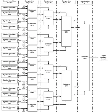
In order to reduce the number of propagation cycles a tree topology of 15 comparators was implemented to pick up the index of the symbol correlator which have the maximum correlation value. In fact, the index of each correlator is a 4 bit binary code that matches a unique 32 bits spreading sequence according to the table III for the option 3PHYlayer. A structure view of the implemented symbol bank correlator and the tree topology of comparators to find maximum value of correlation that match the decoded symbol is illustrated in Fig. 15.
Fig. 14: Bloc diagram of the hardware implementation of the correlation algorithm.
Fig. 15: Structure view of the implemented symbol bank correlator and the tree topology of comparators to find
maximum value of correlation that match the decoded symbol.
IV. IMPLEMENTATIONRESULTS
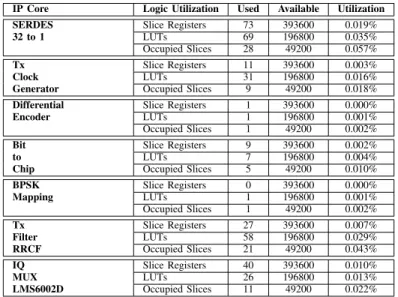
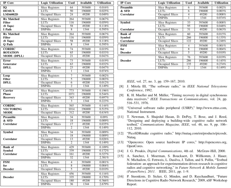
This section presents the performance of the IPs imple-mented. Table IV gives a summary of the resource utilization spent by our IEEE 802.15.4IPs on the XilinxFPGA. Tables V and VI present a detailed description of resource utilization for transmitter option 1/2 and option 3 IPs while Table VII and VIII present resource utilization for the receivers for both option 1/2 and option 3. One can see that Table VII for option 1/2 does not contain all the IPs of the proposed architecture. This is simply due to the fact that many modules are shared between both options. Therefore, to avoid duplication of results we presented the resource utilization for the shared modules only in the Table VIII related to option 3 receiver.
As already explained, the design has been implemented on Nutaq picoSDRplatform which is based on the Perseus 6011 digital domain board with a Virtex-6XC6VSX315T FPGA. Our contribution consists in the design of a multiple PHY layers design of the IEEE 802.15.4 standard, in addition to the TX and RX IPs, the FPGAfabric contains a Microblaze processor
running a PetaLinux operating system aimed to configure
EMAC, EDMA and RTDEx busses and to tune the RF Front-End Radio420 transceiver.
The design methodology was the following: a first Matlab version of the TX and RX flow was functionally validated by Matlab simulation. Then, the IPs where written in register transfer level VHDL, different clock rate could be obtained with a systematic clock enable input for each IP. The net listing process of the IPs was done on Xilinx Platform Studio (XPS), the synthesis place and route were done with Xilinx Synthesis Technology (XST). Simulation was first realized with
matlab version of eachIP, then theVHDLwas simulated using Modelsim and checked with chipscope.
The total user logic IP (i.e. the shaded area on Fig. 6) uses less than 5% of the FPGA. According to table VII we can notice that most of the resource are spent by the receiver. We can observe also that DSP48 resources are mainly used as multipliers to compute energy of preamble, SFD, and symbols inside the decoder. The proposed multiple layer implementa-tion of the IEEE802.15.4 standard requires only fewer number of slices and multipliers compared to the available resources and it does not make use of Block-RAM memories which can be left to more complex design. The higher clock frequency that can be achieved by the implemented IPs is up 200 MHz. Whereas, as explained before, the input clock of this design is provided by the Radio420 front-end receiver in the case of picoSDR node where the maximum sampling frequency is 40 MHz. Therefore, our design can run at least at 80 MHz or higher frequency complying to Shannon theorem. Furthermore, it can be used with RF front-end transceiver which had larger bandwidth up to 100 MHz.
The resource utilization of the implemented IPs shows that designers can think to parallel implementation of much more complex SDR designs on FPGA such as single and multiple carrier baseband communication systems and MIMO
processing.
V. CONCLUSION
The continuing need for high data rateRFtechnologies and
TABLE IV: Device Utilization Table Summary.
IP Core Logic Utilization
Used Available Utilization
Transmitter Slice Registers 150 393600 0.038% Option 1 & 2 Slice LUTs 140 196800 0.071% Occupied Slices 72 49200 0.146% Transmitter Slice Registers 269 393600 0.068% Option 3 Slice LUTs 230 196800 0.117% Occupied Slices 115 49200 0.234% Receiver Slice Registers 1499 393600 0.381% Option 1 & 2 Slice LUTs 1709 196800 0.868% Occupied Slices 652 49200 1.325% DSP48s 23 1344 1.711% Receiver Slice Registers 1879 393600 0.477% Option 3 Slice LUTs 1758 196800 0.893% Occupied Slices 697 49200 1.417% DSP48s 57 1344 4.241% IEEE 802.15.4 Slice Registers 3797 393600 0.964% TX/RX total Slice LUTs 3837 196800 1.949% Occupied Slices 1536 49200 3.122% DSP48s 80 1344 5.958%
TABLE V: Device Utilization Table Summary of the option 1 and 2 transmitter.
IP Core Logic Utilization Used Available Utilization SERDES Slice Registers 73 393600 0.019% 32 to 1 LUTs 69 196800 0.035% Occupied Slices 28 49200 0.057% Tx Slice Registers 11 393600 0.003%
Clock LUTs 31 196800 0.016%
Generator Occupied Slices 9 49200 0.018% Differential Slice Registers 1 393600 0.000% Encoder LUTs 1 196800 0.001% Occupied Slices 1 49200 0.002% Bit Slice Registers 9 393600 0.002%
to LUTs 7 196800 0.004%
Chip Occupied Slices 5 49200 0.010% BPSK Slice Registers 0 393600 0.000% Mapping LUTs 1 196800 0.001% Occupied Slices 1 49200 0.002% Tx Slice Registers 27 393600 0.007% Filter LUTs 58 196800 0.029% RRCF Occupied Slices 21 49200 0.043% IQ Slice Registers 40 393600 0.010% MUX LUTs 26 196800 0.013% LMS6002D Occupied Slices 11 49200 0.022%
to enhance SDRcommunication systems. Up to very recently,
SDR technology was only accessible to restricted
communi-ties and nowadays, it becomes more and more affordable. In addition, FPGAs provide flexibility to achieve SDR signal processing and RF tuning, simultaneously with high levels of performance and cost efficiency. Even ifGNUradio community is opening-up new opportunities to implement SDR design, there is still further needs to make open source hardware designer to re-use their ownIPs for digital-up and digital-down conversion. Therefore, new SDR and cognitive radio testbeds should give an open access supported with open source HDL
design for scientific community. This is the main objective of
CorteXlabtestbed in which context the present work is carried out.
This paper has provided an tutorial approach of how the baseband part of IEEE 802.15.4 standard can be implemented on FPGA target. A multiple PHY layer design was presented to allow experimentation, in CorteXlab testbed, of all the possibilities offered by the standard regardless of regulatory
TABLE VI: Device Utilization Table Summary of the option 3 transmitter.
IP Core Logic Utilization Used Available Utilization Bit Slice Registers 74 393600 0.019%
to LUTs 65 196800 0.033%
Symbol Occupied Slices 21 49200 0.043% Tx Slice Registers 16 393600 0.004%
Clock LUTs 22 196800 0.011%
Generator Occupied Slices 7 49200 0.014% Symbol Slice Registers 73 393600 0.019%
to LUTs 63 196800 0.032%
Chip Occupied Slices 23 49200 0.047% O-QPSK Slice Registers 7 393600 0.002% Mapping LUTs 5 196800 0.003% Occupied Slices 6 49200 0.012% Tx Slice Registers 27 393600 0.007% Filter LUTs 59 196800 0.030% I Path Occupied Slices 23 49200 0.047% Tx Slice Registers 27 393600 0.007% Filter LUTs 59 196800 0.030% Q Path Occupied Slices 23 49200 0.047% IQ Slice Registers 64 393600 0.016%
MUX LUTs 50 196800 0.025%
LMS6002D Occupied Slices 24 49200 0.049%
limits. The design flow and the proposed architecture are generic and hence they can be applied to implement an FPGA -based single carrier communication system on Nutaq and other
SDRplatforms with minor adaptations. We have presented the
FPGAresources occupied by the proposedIPs (less than 5% of theFPGAall together). TheseIPs can ebe re-used by designers to build an open source HDL library for SDRsystems.
As short term perspectives to the proposed receiver archi-tectures, we plan to add anLQI(stands for Link Quality
Indica-tion) IP which purpose aims to compute a measurement char-acterizing the strength and/or quality of a received packet. This measurement may be implemented using receiver ED(Energy Detection), a signal-to-noise ratio estimation, or a combination of these methods. The LQI IP should help performing tests of ACM-based (for Adaptive Coding & Modulation) scenario where modulation switching criteria is based on continuous estimation and monitoring ofSNR. This will allows the system to switch PHY options before errors are detected by the user. Besides, to make our multiple layerHDLimplementation fully compatible with the IEEE 802.15.4 standard, a MAC layer must be co-designed and implemented on both FPGAand the host machine. Currently, we have a very light MAC layer that performs packet building and we are studying the adaptation of TKN15.4, Open-ZB or OpenMAC which are open-source implementations of the IEEE 802.15.4/ZigBee protocol stack targeted tinyos platforms.
Finally, in the context of CorteXlab testbed development, future work will focus on multiple carrier and multiple antenna systems which will bring more open-source design to scientific community. This will enable more understanding of FPGA
implementation of baseband blocks ofPHYlayer and will take advantage of the open access to CorteXlab testbed to test and develop new design while reusing available IPs.
REFERENCES
[1] R. Andraka, “A survey of cordic algorithms for fpga based computers,” in Proceedings of the 1998 ACM/SIGDA sixth international symposium
TABLE VII: Device Utilization Table Summary of the option 3 receiver.
IP Core Logic Utilization Used Available Utilization IQ Slice Registers 64 393600 0.016%
DEMUX LUTs 50 196800 0.025%
LMS6002D Occupied Slices 24 49200 0.049% Rx Matched Slice Registers 264 393600 0.067% Filter LUTs 116 196800 0.059% (8 Taps) Occupied Slices 58 49200 0.118%
I Path DSP48s 8 1344 0.595%
Rx Matched Slice Registers 264 393600 0.067% Filter LUTs 116 196800 0.059% (8 Taps) Occupied Slices 58 49200 0.118%
Q Path DSP48s 8 1344 0.595%
CORDIC Slice Registers 74 393600 0.019% ROTATION LUTs 65 196800 0.033% MODE (DPLL) Occupied Slices 21 49200 0.043% Error Slice Registers 73 393600 0.019% Generator LUTs 63 196800 0.032% DPLL Occupied Slices 23 49200 0.047% DSP48s 1 1344 0.074% Loop Slice Registers 7 393600 0.002%
Filter LUTs 5 196800 0.003%
DPLL Occupied Slices 6 49200 0.012% DSP48s 2 1344 0.149% Carrier Slice Registers 773 393600 0.196% Phase LUTs 1071 196800 0.544% Recovery Occupied Slices 343 49200 0.697% DSP48s 3 1344 0.223% CORDIC Slice Registers 565 393600 0.144% VECTORING LUTs 1014 196800 0.515% MODE Occupied Slices 312 49200 0.634% Preamble Slice Registers 34 393600 0.09% & SFD LUTs 18 196800 0.009% Correlator Occupied Slices 17 49200 0.035% DSP48s 2 1344 0.149% Symbol Slice Registers 34 393600 0.009% LUTs 18 196800 0.009% Correlator Occupied Slices 13 49200 0.026% DSP48s 2 1344 0.149% Bank of Slice Registers 429 393600 0.109% Symbol LUTs 339 196800 0.172% Correlator Occupied Slices 161 49200 0.327% DSP48s 32 1344 2.381% FSM Slice Registers 4 393600 0.001%
for LUTs 8 196800 0.004%
Decoder Occupied Slices 5 49200 0.010% Slice Registers 456 393600 0.116% Decoder LUTs 335 196800 0.170% Occupied Slices 180 49200 0.366% DSP48s 36 1344 2.679%
on Field programmable gate arrays, New York, NY, USA, 1998, pp. 191–200.
[2] K.-C. Chen and J.-M. Lee, “A family of pure digital signal processing bit synchronizers.” IEEE Transactions on Communications, vol. 45, no. 3, pp. 289–292, 1997.
[3] M. Dardaillon, K. Marquet, T. Risset, and A. Scherrer, “Software Defined Radio Architecture Survey for Cognitive Testbeds,” in Wireless
Communications and Mobile Computing Conference (IWCMC), 2012 8th International, Limassol, Cyprus, Sep. 2012.
[4] “Equipex FIT: Future Internet of Things,” http://fit-equipex.fr, French National Research Agency, ANR.
[5] F. M. Gardner, “Interpolation in digital modems. I. Fundamentals,”
Communications, IEEE Transactions on, vol. 41, no. 3, pp. 501–507, Aug. 1993.
[6] “Part 15.4: Wireless Medium Access Control (MAC) and Physical Layer (PHY) Specifications for Low-Rate Wireless Personal Area Networks (WPANs),” IEEE Computer Society, 2006, iEEE Std 802.15.4-2006. [7] M. Mattavelli, I. Amer, and M. Raulet, “The reconfigurable video
coding standard [standards in a nutshell],” Signal Processing Magazine,
TABLE VIII: Device Utilization Table Summary of the option 1 & 2 receiver.
IP Core Logic Utilization Used Available Utilization Preamble Slice Registers 6 393600 0.002% & SFD LUTs 6 196800 0.003% Correlator Occupied Slices 4 49200 0.008% DSP48s 1 1344 0.074% Symbol Slice Registers 33 393600 0.008% LUTs 95 196800 0.048% Correlator Occupied Slices 31 49200 0.063% Bank of Slice Registers 60 393600 0.015% Symbol LUTs 266 196800 0.135% Correlator Occupied Slices 122 49200 0.248% FSM Slice Registers 4 393600 0.001%
for LUTs 8 196800 0.004%
Decoder Occupied Slices 5 49200 0.010% Slice Registers 76 393600 0.019% Decoder LUTs 286 196800 0.145% Occupied Slices 135 49200 0.274% DSP48s 2 1344 0.149%
IEEE, vol. 27, no. 3, pp. 159–167, 2010.
[8] J. Mitola III, “The software radio,” in IEEE National Telesystems
Conference, 1992.
[9] K. H. Mueller and M. M¨uller, “Timing recovery in digital synchronous data receivers.” IEEE Transactions on Communications, vol. 24, pp. 516–531, 1976.
[10] “Universal software radio peripheral (USRP),” http://www.ettus.com, National Instrument.
[11] T. Newman, S. Shajedul Hasan, D. DePoy, T. Bose, and J. Reed, “Designing and deploying a building-wide cognitive radio network testbed,” Communications Magazine, IEEE, vol. 48, no. 9, pp. 106– 112, 2010.
[12] “PicoSDRmake cognitive radio,” http://nutaq.com/en/products/picosdr, Nutaq.
[13] “Opencores: Open source hardware IP cores,” http://opencores.org, OpenCores.
[14] J. G. Proakis, Digital Communications, 4th ed. McGraw-Hill, 2000. [15] A. Sanchez, I. Moerman, S. Bouckaert, D. Willkomm, J. Hauer,
N. Michailow, G. Fettweis, L. Dasilva, J. Tallon, and S. Pollin, “Testbed federation: an approach for experimentation-driven research in cognitive radios and cognitive networking,” in Future Network & Mobile Summit
(FutureNetw), 2011. IEEE, 2011, pp. 1–9.
[16] P. Steenkiste, D. Sicker, G. Minden, and D. Raychaudhuri, “Future Directions in Cognitive Radio Network Research,” 2009, nSF Workshop Report.
![Fig. 1: Hardware/software requirements for the CorteXlab cognitive radio node (figure from [3]).](https://thumb-eu.123doks.com/thumbv2/123doknet/14524962.532211/3.918.513.819.78.283/fig-hardware-software-requirements-cortexlab-cognitive-radio-figure.webp)