Influence of texture on the switching behavior
of Pb(Zr
0.70Ti
0.30)O
3sol-gel derived thin films
Keith G. Brooks, Radosveta D. Klissurska, Pedro Moeckli, and N. Setter
Laboratoire de C´eramique, Ecole Polytechnic F´ed´erale de Lausanne, Lausanne, Switzerland (Received 1 August 1995; accepted 22 August 1996)
Rhombohedral Pb(Zr0.70Ti0.30)O3 thin films of four different well-defined textures,
namely, (100), (111), bimodal (110)y(111), and (100)y(111), were prepared by a sol-gel method. The films were characterized in terms of grain size, presence of second phases, surface roughness, columnarity of grains, and other microstructural features. The dielectric, ferroelectric, and fatigue properties were investigated, with emphasis on the hysteresis switching characteristics. Results are discussed from the reference point of the allowable spontaneous polarization directions available for the different textures. The values of coercive field, remanent and saturation polarization, and slope of the loop at the coercive field, at saturating fields can be qualitatively explained based on the texture, independent of microstructural differences. The occurrence of surface pyrochlore, however, is observed to affect the functionality of the saturation curves, particularly for the samples of bimodal texture. Shearing of the hysteresis curves of the bimodal films is also attributed to surface microstructural features. The occurrence of nonswitching 71±or 109±domains in the (111) and (110)y(111) textured films is hypothesized based on a comparison with the data from the (100) textured film. Corrected saturation polarization values agree with the spontaneous polarization values of rhombohedral PZT single crystals and published calculated values for rhombohedral PZT ceramics. The fatigue characteristics show increases in the switching component of polarization in the range 103– 107 bipolar cycles, particularly for the (111) textured sample. Onset of fatigue is
observed for all samples between 107 and 108 switching cycles.
I. INTRODUCTION
Pb(Zr12xTix)O3 thin films have been studied
inten-sively during the past decade for nonvolatile ferroelectric memory applications.1 A majority of the investigations
have centered around compositions in close proximity to the rhombohedral/tetragonal morphotropic boundary at x ø 0.47.2 The morphotropic composition and those
to the tetragonal side of it sx . 0.47d are interesting, as maximum values of remnant polarization sPrd are
observed.3–6 Softer hysteresis with lower P
r and
coer-cive field sEcd occurs for rhombohedral compositions
sx , 0.47d.2–4,6–8Rhombohedral compositions thus have
the advantage of lower switching fields.3
In the preparation of PZT thin films by various dep-osition techniques, it has been reported that the ease of nucleation of the perovskite structure improves with Ti addition. Typically in rhombohedral (Zr-rich) films, rosette-type microstructures are observed (particularly for sol-gel derived films) due to the higher perovskite nucleation energy and the increased stability of the py-rochlore phase.9,10 Similar microstructural features have
also been observed for rhombohedral Pb(Zr0.65Ti0.35)O3
prepared by reactive dc-magnetron sputtering and crys-tallization ex situ.8 In sol-gel deposition where ex situ
crystallization is required, these two factors strongly influence the PZT microstructure due to the need for efficient nucleation of the perovskite phase (high nuclei density) and the amorphous to pyrochlore to perovskite crystallization sequence.11–14
Several recent papers discuss the effects of micro-structure and texture (“epitaxy”) on the switching and fatigue properties of PZT thin films.15 In this work,
the term texture is used to describe films of columnar structure that show a preferred growth direction with respect to the z-axis (substrate normal) and a random orientation in the x-y plane (plane of film) as dis-cussed in greater detail below. Bellur et al. investigated polycrystalline films of the morphotropic composition deposited on Pt electrodes and being either randomly oriented or (001) textured (“epitaxial”) prepared on Pt on MgO. The (001) textured film was observed to exhibit squarer hysteresis loops. This work indi-cated that for films of different orientation, the ability to “rejuvenate” (with dc voltage) a fatigued capacitor was favored in the case of the highly (001) oriented film. The authors have excluded a priori in their dis-cussion the possibility of rhombohedral-type grains or domains.
Tuttle et al.16,17 discussed films of rhombohedral
60y40 composition prepared on platinum-coated (0001) sapphire and (100) Si substrates. The larger remanent polarizations and squarer loops achieved in the films on sapphire were attributed to the films being in compres-sive stress during cooling through the Curie temperature, thus yielding more domains oriented in the direction of the applied field.
Larsen et al. investigated the switching times of PZT thin films as a function of film morphology and possible domain structure.18 It was observed that the fastest switching occurred when the films were of columnar microstructure (i.e., with no grain boundaries parallel to the substrate). It is argued that either a domain nucleation dominated switching or bulk effect switching occurs.
In this work, the effects of film orientation on the dielectric, switching, and fatigue behavior of sol-gel Pb(Zr0.70Ti0.30)O3 films prepared on PtyTiySiO2ySi
sub-states has been investigated. Film microstructures were characterized in detail in order to isolate the orientation effects. The rhombohedral composition was chosen, as the spontaneous polarization directions are well defined compared to the near morphotropic compositions. II. EXPERIMENTAL
A. Film preparation and microstructural characterization
Pb(Zr0.70Ti0.30)O3 thin films were prepared by a
modified sol-gel method.13,19 To compensate for lead loss during Rapid Thermal Annealing (RTA), 15 mol % excess lead was added to the precursor solution. Details of the processing have previously been reported, and
thus only a brief description is given here.13 Pb
acetate ? 3H2O was dissolved in 2-methoxyethanol,
dried by vacuum distillation, and then redissolved in 2-methoxyethanol. Separately a solution of Zr n-propoxide and Ti ison-propoxide in 2-methoxyethanol was prepared in a dry nitrogen glovebox. This solution was then added to the Pbymethoxyethanol solution, allowed to reflux at 120±C for 1 h at 500 mbar pressure, and then distilled to achieve a concentration .0.4 M. The final 0.4 M stock solution was obtained by dilution with 2-methoxyethanol. Formamide, a drying control addi-tive, in the quantity of 4 vol % was then added to the stock solution.
Thin films were prepared on Si substrates with SiO2 (1000 nm), Ti (10 nm), and Pt (100 nm) layers
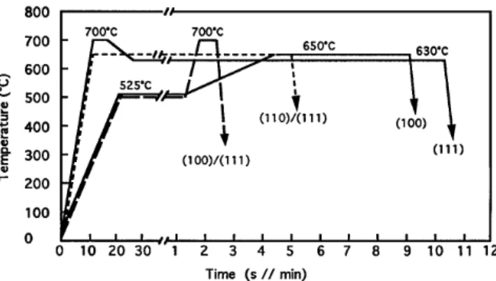
by successive spin coating steps. Five layers of sol-precursor were deposited with a 350±C pyrolysis treat-ment between each to yield a PZT film after annealing of ø0.3 mm thickness. Different RTA profiles were employed to achieve different film textures. The effect of annealing and pyrolysis treatment on sol-gel PZT nucleation, growth, and film texture has been previously
FIG. 1. Graph showing the programmed rapid thermal annealing profiles employed to obtain the different PZT film textures.
reported in detail.14,20Programmed rapid thermal heating
profiles used to achieve the four different thin film textures reported herein are presented in Fig. 1. The true thermal profiles deviate from the programmed ones, particularly during the cooling ramp(s).
The diffraction spectra were acquired using Cu Ka
radiation on a u-2u diffractometer (D-500, Siemens, Germany) equipped with a diffracted beam poly-crystalline graphite monochometer and a scintillation counter. To quantify the degree of preferred orientation in the different film samples, the method proposed by Harris21 (later corrected by Barrett22) for inverse pole figures was used. The integrated intensities were obtained by fitting the measured peaks with Cauchy-like functions. Functions with more parameters (e.g., Split Pearson) did not yield significantly better R-values. The necessary randomly oriented sample was prepared from the same sol-gel precursor as the films. Due to the high symmetry of the samples, overlaps with peaks of other phases (Pt, Si), and the sharpness of the preferred orientation, only a very restricted number of peaks could be used to quantify the texture (see Table I). As the precision of the Harris method increases with increasing number of available peaks, the results given in Table I must be considered to be only semiquantitative. In Table I, the percentage values given indicate the volume percent of the film which is of a given orientation. Specifically, the values were obtained as: Volume %
shkld fsIf ,hklyIp,hkldy
P
sIf,hklyIp,hkldg 3 100, where I
is the integrated intensity, f indicates film, p the randomly oriented powder sample, and the summation is over all of the measured reflections.
The microstructure of the PZT film surfaces (as-prepared) was investigated by scanning electron micros-copy (SEM) (JEOL 6300, Japan) using an accelerating voltage of 3 – 6 kV. Atomic force microscopy (AFM) was utilized to aid in the interpretation of the SEM images and extract further information about the respec-tive microstructures. The microstructures in transverse
TABLE I. Summary of XRD diffraction results for quantitative texture analysis of PZT films. Intensity and texture data
Powder (100) (111) (100)y(111) (111)y(110)
Peak Intensity Intensity % Intensity % Intensity % Intensity %
100 208 2802 49 185 15 200 453 4805 æææ 97 52 æææ ,1 205 æææ 50 14 æææ 9 110 1414 4 149 164 154 220 261 0 æææ 1 13 æææ 1 10 æææ 5 10 æææ 13 111 152 64 4467 118 79 222 70 23 æææ 2 900 æææ 98 22 æææ 41 23 æææ 75 210 162 0 0 0 0 0 0 0 0 211 727 0 0 15 ,1 33 2 24 3 221 1 300 71 a a a a 310 215 0 0 14 ,1 7 1 0 0 320 34 b b b b 321 278 b b b b
aNo reliable data due to overlap with Si 400 peak. bNo reliable data due to overlap with strong Pt 222 peak.
section were studied by transmission electron mi-croscopy (TEM) (EM 430, Philips, Holland).
B. Electrical measurements
The dielectric properties of the films were char-acterized using a network analyzer (Hewlett-Packard HP4190A) at 10 kHz and 50 mV oscillation level. The switching characteristics of each film were measured using commercial test equipment (RT66A, Radiant Technologies). Saturation characteristics were obtained by measuring hysteresis loops with increasing applied field at 50 kVycm increments. For each increment, first a positive (1 on top electrode) and then a negative loop were acquired. The following characteristics of the loops were extracted as a function of increasing field: average coercive field fsj1 Ecj 1 j2 Ecjdy2g, hysteresis slope
at 2Ec for positive loop fs≠Py≠Ed2Ecg, saturation po-larizationsPsd, and average remanent polarization sPrd.
Fatigue was measured for each sample at two differ-ent fields, 150 and 300 kVycm (or approximately 5 and 10 volts). The measurement frequency was 30 kHz and each film was measured to 108 cycles.
III. RESULTS AND DISCUSSION A. Microstructural characterization
Results from the semiquantitative XRD texture analysis are presented in Table I. Two strongly textured films being (100) and (111) oriented and two films of bimodal texture, (110)y(111) and (100)y(111), were investigated. Although pyrochlore could not be detected by XRD, the occurrence of pyrochlore on the surfaces of all films was observed by SEM and TEM as discussed below.
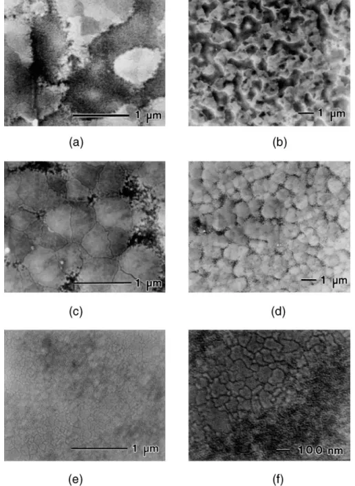
Characteristic SEM images are shown in Fig. 2. The surface of the (100) textured film is characterized by two different contrasts, the darker being attributed to residual pyrochlore (covering approximately half of the film surface), and the lighter being perovskite structured phase. The perovskite phase areas are divided by grain and/or subgrain boundaries which indicate a grain size in the range of 0.2 and 0.6 mm. The (111) textured film has a similar microstructure, with the exception that much less pyrochlore is observed. In the (111) case, the pyrochlore is observed to be located preferentially at grain boundaries. Very different microstructures were observed for the films of bimodal texture. Both exhibited similar microstructures, with grain sizes significantly smaller than those of the (100) and (111) films, falling in the range 0.05– 0.1 mm. Similar to the (100) textured film, pyrochlore was observed to cover approximately 40% of the films surface by image analysis.
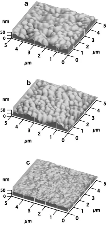
AFM results are shown in Fig. 3. It was observed that the (100) and (111) textured films have much rougher surfaces than the films of bimodal texture, with deviations being on the order of 30 nm, compared to 5 nm, respectively. By comparison with the SEM results, the pyrochlore which occurs on the surface of the (111) and to some extent in the (100) textured films is located in depressed regions between grains.
TEM analysis indicated that all of the films investi-gated exhibited columnar microstructures, such that all observed grain boundaries were essentially perpendicular to the substrate surface. The thickness of the pyrochlore on the film surfaces, as noted above, was found to be of the order of a few nanometers.
The perovskite structure nucleates at the film/bottom electrode interface in each case.13,14 Essentially, the
FIG. 2. SEM images of the surfaces of (a) and ( b) (100), (c) and (d) (111), and (e) and (f) (110)y(111) textured films. Note, the surface microstructure of the (100)y(111) film was similar to the (110)y(111) film.
two interactive factors, being the free energy of growth in a given direction and influences of the PZT/bottom electrode interface. Although the different orientations were achieved empirically, the following ideas aided in reducing the number of annealing trials to achieve such textures. It is known that the (100) face of the perovskite lattice is neutral and thus should be the fa-vored growth plane in the absence of other influences. Secondly, it has been reported in several papers that for sol-gel preparation of PZT films, an amorphous to metastable pyrochlore to perovskite crystallization
sequence occurs.11–14 The ease of formation of the
per-ovskite nuclei thus is dependent upon the stability of the transient pyrochlore phase. Further, it has been reported that the stability of the pyrochlore phase increases with increasing Zr concentration, often leading to rosette type microstructures for rhombohedral compositions.9,10 The
influence of the substrate, and in particular the TiyPt bilayer metallization, further complicates the perovskite nucleation energetics. Numerous papers report that (111) oriented PZT nuclei form at the PtyPZT interface due to a close lattice match between the (111) planes of the
FIG. 3. AFM images of the surfaces of (a) (100), ( b) (111), and (c) (110)y(111) textured films.
two materials. This effect is further enhanced by the occurrence of Pb – Pt alloys,23Pb –Ti alloys,24 and/or the
presence of Ti or TiO225–27 at the PZTyPt interface, all
of which can act to further reduce the lattice mismatch. In this case, a strongly oriented Pt electrode is required. An unequivocal explanation for the textures achieved in this work cannot be given because the perovskite nucleation and changes in the TiyPt bottom electrode structure (e.g., Ti diffusion through Pt and concurrent oxidation of the Ti) occur simultaneously. However, the
following general explanation holds. For the (111) case, the film is heated very rapidly to 700±C, thus passing through the pyrochlore transition rapidly and favoring nucleation by lattice matching with the Pt electrode with one or more of the above-mentioned events (e.g., formation of Pb – Pt alloy). For the (100) film, heating is slower and the perovskite grains are nucleated at a lower temperature (525±C), where the free energy of the perovskite lattice dictates the nuclei stability. Here, also, the perovskite nucleation occurs simultaneously with the pyrochlore phase crystallization. The two films of mixed texture were prepared by using annealing profiles which fall between these two extreme cases.
B. Dielectric properties
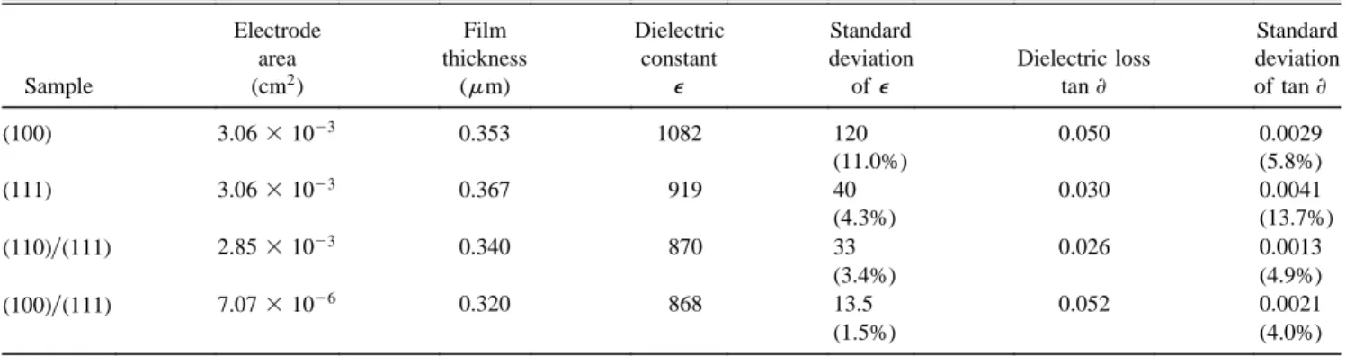
The measured capacitor thickness, electrode area, dielectric constant, and loss data are given in Table II. The values of the dielectric constants obtained for the (110)y(111) and (100)y(111) samples of 876 and 868, respectively, compare with that of approximately 840 re-ported by Watanabe et al. (measurement field: 200 mV).4
Diffraction data were not reported by Watanabe; how-ever, data for a film of Pb(Zr0.80Ti0.20)O3 composition
were given, and were of mixed orientation with (100) and (111) reflections being the strongest [preferred ori-entation is implied because for a powder pattern, the (110) reflection is strongest]. Considering one standard deviation for 10 measurements, the (100) film exhibits the highest dielectric constant, followed by the (111), with the (110)y(111) and (100)y(111) samples being nominally the same. There is a clear difference in the
tan d values, with the (100) and (100)y(111) samples
showing a loss of approximately 5%, being approxi-mately twice that of the (110)y(111) and (111) cases. C. Switching parameters
Virgin hysteresis loops taken at 300 kVycm applied fields and a frequency of 50 Hz are shown in Fig. 4, for each of the films investigated. It is observed that loops for the (100) and (111) textured films are very symmetric, with the (111) exhibiting a much larger Ps
compared to the (100). The films of bimodal texture are asymmetric by comparison, being shifted toward posi-tive field. The saturation polarization of the (110)y(111) and (100)y(111) textured films fall between those of the (100) and (111) films. Constriction of the center part of the hysteresis loops of the (111) and (110)y(111) films is also apparent in Fig. 4. Such a phenomenon has been previously reported for rhombohedral phase PZT thin films [Pb(Zr0.65Ti0.35)O3], being explained as
“hystere-sis relaxation.”8 In bulk ceramics, such constrictions of
the hysteresis loops and a concurrent reduction of the dielectric loss factor, tan d, occur with aging due to a gradual stabilization of the domain structure.28 The
TABLE II. Summary of the dielectric property measurements.
Electrode Film Dielectric Standard Standard
area thickness constant deviation Dielectric loss deviation
Sample (cm2) (mm) e of e tan ≠ of tan ≠
(100) 3.06 3 1023 0.353 1082 120 0.050 0.0029 (11.0%) (5.8%) (111) 3.06 3 1023 0.367 919 40 0.030 0.0041 (4.3%) (13.7%) (110)y(111) 2.85 3 1023 0.340 870 33 0.026 0.0013 (3.4%) (4.9%) (100)y(111) 7.07 3 1026 0.320 868 13.5 0.052 0.0021 (1.5%) (4.0%)
constriction can be removed either by application of a strong ac field or by heating above the Curie tem-perature. It is noted that the two films that show some constriction in the virgin hysteresis loops also exhibit much lower ( by approximately 50%) tan d values than the (100) and (100)y(111) films. Several mechanisms have been proposed to explain such effects in bulk ce-ramics as discussed by, e.g., Lambeck and Jonker.28
The mechanisms involve one or more of the following phenomenon: stabilization of the existing spontaneous polarization direction due to anisotropic lattice defects, pinning of domain walls by diffusing lattice defects, cre-ation of internal electric field due to discontinuities in the spontaneous polarization within the material, and stress effects. The possibilities that are most likely re-sponsible for the constrictions observed are stress or grain size effects. Finally, it is noted that all of the loops have some shear characteristic, as defined by
FIG. 4. Virgin hysteresis loops of the (a) (100), ( b) (111), (c) (110)y (111), and (d) (100) (111) films.
Arlt,29whereby the loop appears tilted, but the saturation
polarization is essentially unaffected. The occurrence of surface pyrochlore is one factor that is known to cause such a shear phenomenon.30
As a preface to describing the hysteresis satura-tion characteristics, a short discussion of the possible orientations of the spontaneous polarization vectors in the four films studied follows. First, it is noted that in the plane of the film, there is no preferred orientation. This was shown experimentally by x-ray diffraction, by rotating the sample in the plane at increments of 10± and collecting diffraction data for given reflections. No change of intensity was observed as a function of rotation angle. For the (100) case, a single polarization direction exists relative to the plane of the electrode (positive or negative directions, making an angle of ø35± to
the substrate surface). For the (111) and (100)y(111) films, two possible directions exist, being oriented at 35± and 90±to the substrate. Four equivalent directions are possible in the (110)y(111) case, having angles of 0, 35, 54, and 90±.
The hysteresis saturation characteristics for the different textures are considered in detail next. The first parameter to be addressed is Ps, with data summarized in
Fig. 5. It was observed that the saturation polarizations
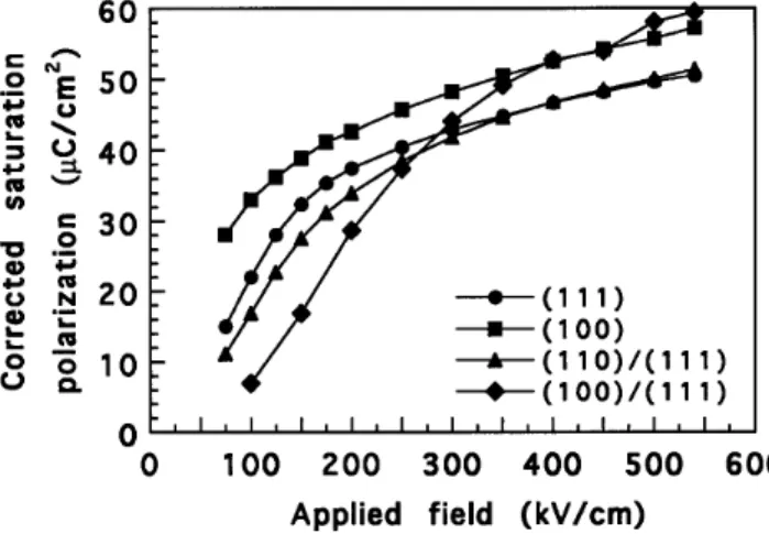
for the differently textured films, at all fields above 175 kVycm, respectively, increase in the order (100), (100)y(111), (110)y(111), and (111). The low values of the polarization for the (100) sample cannot be explained by the presence of pyrochlore on the film surface, as the hysteresis saturates at very low fields compared to the other three films, and the two films of bimodal texture contain qualitatively similar quantities of pyrochlore. Considering that the spontaneous polarization vectors are constrained to be at an angle of 54±to the substrate, the measured maximum polarization of the (100) oriented films is expected to be at most 57.7% of the true spontaneous polarization, with the value being further reduced if nonswitching 109±or 71±domains are present. In order to ascertain the values of spontaneous polarization for the different films, correction factors were applied to the measured values. For the (100) film, all values were multiplied by 1.74, in order to correct for the angle between the applied field and the spontaneous polarization direction. Corrections were applied for the other three films based on the quantitative XRD results, using the following assumptions: (i) for the (111) film, no correction is applied; i.e., it is assumed that (at high fields) all of the spontaneous polarization vectors are perpendicular to the plane of the films; (ii) for the (110)y(111), it is assumed that the polarization vectors at high field lie in the direction closest to being perpendicular to the plane; and (iii) for the (100)y(111) film, correction was only made for the (100) grains, with assumption (i) holding for the (111) grains. The results are shown in Fig. 6. At saturating fields, it is clear that with the corrections, the polarization values in the (100) and (100)y(111) films are identical, and approach values of 55– 60 mCycm2. For poor quality single
crystals of rhombohedral PZT compositions near the morphotropic phase boundary, values of spontaneous
polarizations of 50 mCycm2 have been reported.3
FIG. 6. Saturation polarization as a function of applied field corrected to show spontaneous polarization values. See text for details.
Jaffe et al. have calculated, based on measurements of rhombohedral ceramics, that the saturation polarization
should approach 55 mCycm2. These values are in
agreement with those obtained by applying the above corrections to the (100) and (100)y(111) films, indicating that the stated assumptions hold. For the (100) case, this also indicates that if 79±or 109±domain walls exist in the virgin films, they are consumed at saturation. Again considering the corrected saturation curves shown in Fig. 6, the (111) and (110)y(111) films exhibit lower values of polarization. This would indicate that the first assumption stated above is not entirely valid, i.e., some of the polarization vectors (domains) lie in the off-axis position, and some or all of these do not switch. Thus, the volume fraction of material with nonswitching off-axis domains was calculated in order to obtain coincidence of the Ps saturation curves with the corrected curve for
the (100) sample. It was found that the spontaneous polarization of 15% of the (111) grains [or 15 vol % of the (111) oriented material] must be retained in the off-axis position, to achieve coincidence with the (100) textured film. With such an additional correction [applied to both the (111) and (110)y(111) films], all four of the saturation curves become coincident above 350 kVycm, as shown in Fig. 7. At fields below 350 kVycm, the surface pyrochlore causes a shift of the saturation curves toward larger field. This analysis indicates that these two films do not switch completely under the test con-ditions used.
Saturation curves of Pr are presented in Fig. 8. At
high fields (.350 kVycm), the measured values of Pr
increased in the order (100), (100)y(111), (110)y(111), and (111). It is noted that Prdoes not saturate in a
well-defined way, by comparison with the saturation curves for Ps, particularly for the samples of bimodal texture.
This, again, can partly be explained by the presence of pyrochlore on the film surfaces.30
FIG. 7. Saturation polarization as a function of applied field with correction added, assuming the presence of domains that do not fully switch in the (111) and (110)y(111) textured films. See text for details.
FIG. 8. Average remanent polarization as a function of applied field.
The third hysteresis parameter to be considered is the saturation of the average coercive field, Fig. 9. The lowest coercive field was measured on the (100) textured thin film with increasing coercivities in the order (111), (110)y(111), and (100)y(111), respectively. For the (100) case, the effective field is reduced due to the angle of the spontaneous polarization with respect to the applied field. However, in this case, a single well-defined spontaneous polarization direction exists with respect to the applied field, and thus 180± switching of these domains yields a low coercive field, contrary to the expected increase. Further, it is reasonable to assume that in the (111), (100)y(111), and (110)y(111) textured films there exists in the virgin films domains oriented at an angle of 35± [(100) and (111) grains] or 0± [(110) grains] to the film surface which require a stronger field to switch, assuming either 180±and/or 71y109± switching. Such an assumption is supported by the fact that often the films have a residual tensile stress which would favor the formation of such off-axis domains,16,17 and the analysis of the saturation of Ps, presented above. The high coercive fields observed
FIG. 9. Average coercive field as a function of applied field.
for the films with bimodal textures could have several origins, including stress effects, the occurrence of more complex domain structures due to the increased number of possible domain orientations, and fine grain size, or be primarily due to the smaller grain sizes observed in these films.16,17,29
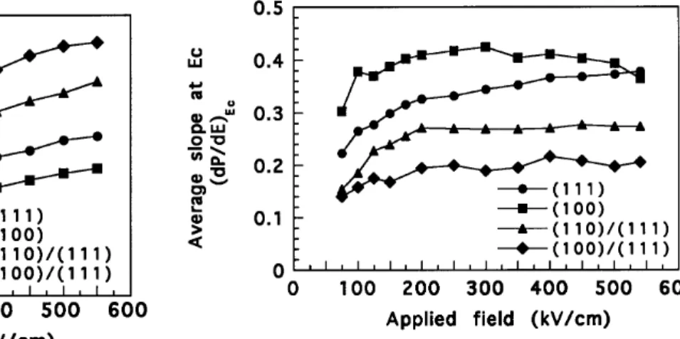
Next, the slope of the hysteresis loop at 2Ec,
Fig. 10, is considered. This parameter is a qualitative measure of the switching efficiency, or the narrowness of the distribution of applied fields within which most of the domains are switched. Here it is observed that the (100) oriented film switches most efficiently, followed by the (111), (110)y(111), and (100)y(111) films. Thus it can be assumed that the threshold field to switch domains in the (100) case is well defined. This is a further indication that the population of 71y109± domain walls is quite low in this sample. For the films of bimodal texture, the slope should be decreased, as the threshold switching field for domains of different orientations will differ, thus causing a broadening of the distribution of switching fields. Again, surface pyrochlore could also contribute to this, as the field seen by the ferroelectric will be different depending on the presence or absence of surface pyrochlore, and the thickness of the nanocrystalline pyrochlore regions.
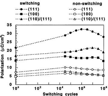
D. Fatigue
Results on the fatigue characteristics are presented in Fig. 11, for fatigue fields of 300 kVycm. All of the fatigue curves are characterized by an initial in-crease in the switched polarization, until approximately 106– 107 cycles, accompanied by an essentially constant
nonswitching component. The increase in switched po-larization is most pronounced for the (111) textured film. One possibility is that domains that initially do not switch, as hypothesized above, become switchable after fatigue cycling. For all films, the switching component begins to decay above 107 cycles. Shepherd reported
FIG. 10. Average slope of the hysteresis loops at Ec as a function
FIG. 11. Typical fatigue curves showing the switched and non-switched components as a function of logsNd, where N is the number of bipolar switching cycles. Films fatigued at 300 kVycm.
similar characteristic phases of fatigue measured on sol-gel Pb(Zr0.50Ti0.50)O3 thin films.2 Further investigations
are needed to determine if texture has an influence on fatigue mechanisms.
IV. CONCLUSIONS
Rhombohedral Pb(Zr0.70Ti0.30)O3 thin films of the
following different textures, (100), (111), bimodal (110)y(111), and (100)y(111), were investigated. It was found that despite some microstructural differences between them, the switching saturation characteristics could be linked to the film textures and moreover to the spontaneous polarizations directions as defined by the textures. Concerning the switching characteristics, the unique polarization direction existing in the (100) textured films leads to a reduction of the observed coercive field compared to the bimodal and (111) texture cases. The maximum and switchable polarizations are larger in the bimodal and (111) films at high fields (.200 kVycm) when compared to the (100) case. This is attributed to the component of the polarization in the direction of the applied field being larger in these two cases, considering nearly complete switching.
Fatigue results indicate that for all cases an ini-tial increase in polarization occurs for switching cycles
,107. This is attributed to improved domain wall
mo-bility, as it was observed that the hysteresis loops also improve. A second phase of fatigue occurs for N . 106,
where a strong decrease with logsNd is observed. It is shown that some insight into the domain config-urations which exist in PZT thin films can be gained from
studies of films of different textures without direct exper-imental observation of the domains. Information about the domain structures and their influence on ferroelectric, dielectric, and piezoelectric properties of PZT thin films is essential for understanding the performance character-istic of thin film devices based on such materials. ACKNOWLEDGMENTS
The authors gratefully acknowledge I. Reaney for the TEM analysis, and J. Castano for SEM analysis and for AFM. This work was supported by the Swiss gov-ernment through the M2S2 (groupement de laboratoires pour la microm´ecanique sur silicium en suisse) program. This work was initiated as part of the European ESPRIT program FELMAS, and the substrates were provided by Thomson Electronics, Paris, France, a partner in the FELMAS program.
REFERENCES
1. C. A. Paz de Araujo, L. D. McMillan, B. M. Melnick, J. D. Cuchiaro, and J. F. Scott, Ferroelectrics 104, 241 – 256 (1990). 2. W. H. Shepherd, in Ferroelectric Thin Films, edited by E. R.
Myers and A. I. Kingon (Mater. Res. Soc. Symp. Proc. 200, Pittsburgh, PA, 1990), pp. 277 – 288.
3. B. Jaffe, W. Cook, and H. Jaffe, Piezoelectric Ceramics (Aca-demic Press, New York, 1971).
4. H. Watanabe, T. Mihara, and C. A. Paz de Araujo, Proc. 3rd Int. Symp. on Int. Ferroelectrics, Colorado Springs, CO (1991), pp. 139 – 150.
5. J. M. Benedetto, R. A. Moore, and F. B. McLean, J. Appl. Phys.
75, 460 – 466 (1994).
6. B. M. Melnick, C. A. Paz de Araujo, L. D. McMillan, D. A. Carver, and J. F. Scott, Ferroelectrics 116, 79 – 92 (1991). 7. W. Zhu, R. W. Vest, M. S. Tse, M. K. Rao, and Z. Q. Liu, Journal
of Materials Science: Materials in Electronics (Chapman and Hall, New York, 1994), Vol. 5, pp. 173– 179.
8. V. Chikarmane, J. Kim, C. Sudhama, J. Lee, A. Tasch, and S. Novak, J. Electron. Mater. 21, 503 – 512 (1992).
9. L. N. Chapin and S. A. Myers, in Ferroelectric Thin Films, edited by E. R. Myers and A. I. Kingon (Mater. Res. Soc. Symp. Proc.
200, Pittsburgh, PA, 1990), pp. 153 – 158.
10. S. A. Myers and L. N. Chapin, in Ferroelectric Thin Films, edited by E. R. Myers and A. I. Kingon (Mater. Res. Soc. Symp. Proc.
200, Pittsburgh, PA, 1990), pp. 231 – 236.
11. B. A. Tuttle, R. W. Schwartz, D. H. Doughty, and J. A. Voight, in Ferroelectric Thin Films, edited by E. R. Myers and A. I. Kingon (Mater. Res. Soc. Symp. Proc. 200, Pittsburgh, PA, 1990), pp. 159 – 165.
12. C. K. Kwok and S. B. Desu, in Ferroelectric Thin Films II, edited by A. I. Kingon, E. R. Myers, and B. Tuttle (Mater. Res. Soc. Symp. Proc. 200, Pittsburgh, PA, 1992), pp. 159 – 165.
13. I. M. Reaney, K. Brooks, R. Klissurska, C. Pawlaczyk, and N. Setter, J. Am. Ceram. Soc. 77 (5), 1209 – 1216 (1994). 14. K. G. Brooks, I. M. Reaney, R. Klissurska, Y. Huang, L. Bursill,
and N. Setter, J. Mater. Res. 9, 2540 – 2553 (1994).
15. K. R. Bellur, H. N. Al-Shareef, S. H. Rou, K. D. Gifford, O. Auciello, and A. I. Kingon, Proc. ISAF’92, IEEE, 448 – 451 (1992).
16. B. A. Tuttle, J. A. Voigt, T. J. Garino, D. C. Goodnow, R. W. Schwartz, D. L. Lamppa, T. J. Headley, and M. O. Eatough,
Proc. 8th Int. Symp. Appl. Ferroelectrics, Greenville, SC, Aug. 31 – Sept. 2, 1992, pp. 344 – 348.
17. B. A. Tuttle, T. J. Garino, J. A. Voigt, T. J. Headley, D. Dimos, and M. O. Eatough, in Science and Technology of Ferroelectric Thin Films (Kluwer Academic Publishers, The Netherlands, 1995), pp. 117 – 132.
18. P. K. Larsen, G. L. M. Kampsch¨oer, M. B. van der Mark, and M. Klee, Proc. 8th Int. Symp. Appl. Ferroelectrics, Greenville, SC, Aug. 31 – Sept. 2, 1992.
19. K. D. Budd, S. K. Dey, and D. A. Payne, Brit. Ceram. Proc. 36, 107 – 121 (1985).
20. K. G. Brooks, in Growth and Applications of Thin Films, edited by L. Eckertova and T. Ruzicka, Proc. Int. Summer School, June 20 – 25, 1994, Chlum u Trebone, Czech Republic (Prometheus Publishing, Prague, 1994).
21. G. B. Harris, Philos. Mag. 43, 113 (1952).
22. C. S. Barrett, Structure of Metals (McGraw-Hill, New York, 1953), pp. 203 – 205.
23. S. Chen and I. Chen, IMF Proc., August (1993).
24. T. Tani, Z. Xu, and D. A. Payne, in Ferroelectric Thin Films III, edited by E. R. Myers, B. A. Tuttle, S. B. Desu, and P. K.
Larsen (Mater. Res. Soc. Symp. Proc. 310, Pittsburgh, PA, 1993), pp. 269 – 274.
25. M. Klee, A. De Veirman, P. Van de Weijer, U. Mackens, and H. Van Hal, Philips Res. Rep. 47, 263 (1993).
26. G. A. C. M. Spierings, J. B. A. van Zon, M. Klee, and P. K. Larsen, Proc. 4th Int. Symp. on Integrated Ferroelectrics, Monterey, CA, March 9 – 11, 1992.
27. V. Kaushik, P. Maniar, A. Campbell, R. Jones, R. Moazzami, C. J. Mogab, R. Hance, and R. Pyle, in Ferroelectric Thin Films III, edited by E. R. Myers, B. A. Tuttle, S. B. Desu, and P. K. Larsen (Mater. Res. Soc. Symp. Proc. 310, Pittsburgh, PA, 1993), pp. 209 – 214.
28. P. V. Lambeck and G. H. Jonker, Ferroelectrics 22, 729 – 731 (1978).
29. G. Arlt, in Science and Technology of Ferroelectric Thin Films (Kluwer Academic Publishers, The Netherlands, 1995), pp. 261 – 267.
30. A. K. Tagantsev, M. Landivar, E. Colla, K. G. Brooks, and N. Setter, in Science and Technology of Ferroelectric Thin Films (Kluwer Academic Publishers, The Netherlands, 1995), pp. 301 – 314.