HAL Id: hal-02161140
https://hal-univ-rennes1.archives-ouvertes.fr/hal-02161140
Submitted on 1 Jul 2019HAL is a multi-disciplinary open access archive for the deposit and dissemination of sci-entific research documents, whether they are pub-lished or not. The documents may come from teaching and research institutions in France or abroad, or from public or private research centers.
L’archive ouverte pluridisciplinaire HAL, est destinée au dépôt et à la diffusion de documents scientifiques de niveau recherche, publiés ou non, émanant des établissements d’enseignement et de recherche français ou étrangers, des laboratoires publics ou privés.
Finite Size Effects on the Switching Dynamics of
Spin-Crossover Thin Films Photoexcited by a
Femtosecond Laser Pulse
Karl Ridier, Alin-Ciprian Bas, Victoria Shalabaeva, William Nicolazzi, L.
Salmon, Gábor Molnár, Azzedine Bousseksou, Maciej Lorenc, Roman Bertoni,
E. Collet, et al.
To cite this version:
Karl Ridier, Alin-Ciprian Bas, Victoria Shalabaeva, William Nicolazzi, L. Salmon, et al.. Finite Size Effects on the Switching Dynamics of Spin-Crossover Thin Films Photoexcited by a Femtosecond Laser Pulse. Advanced Materials, Wiley-VCH Verlag, 2019, 31 (25), pp.1901361. �10.1002/adma.201901361�. �hal-02161140�
Finite size effects on the switching dynamics of spin-crossover thin films photo-excited by a femtosecond laser pulse
Karl Ridier, Alin-Ciprian Bas, Victoria Shalabaeva, William Nicolazzi, Lionel Salmon, Gábor Molnár,* Azzedine Bousseksou, Maciej Lorenc,* Roman Bertoni, Eric Collet, and Hervé Cailleau
Dr. K. Ridier, Dr. A.-C. Bas, Dr. V. Shalabaeva, Dr. W. Nicolazzi, Dr. L. Salmon, Dr. G. Molnár, Dr. A. Bousseksou
Laboratoire de Chimie de Coordination, CNRS & Université de Toulouse, 31077 Toulouse, France
E-mail: gabor.molnar@lcc-toulouse.fr
Prof. H. Cailleau, Dr. R. Bertoni, Prof. E. Collet, Dr. M. Lorenc
Univ. Rennes, CNRS, IPR (Institut de Physique de Rennes) – UMR 6251, F-35000 Rennes, France
E-mail: maciej.lorenc@univ-rennes1.fr
Keywords: photoswitching dynamics, spin crossover, thin films, size reduction effects, femtosecond optical spectroscopy
Using ultrafast optical absorption spectroscopy, we have studied the room-temperature spin-state switching dynamics induced by a femtosecond laser pulse in high-quality thin films of the molecular spin-crossover complex [Fe(HB(tz)3)2] (tz = 1,2,4-triazol-1-yl). These measurements
reveal that the early, sub-picosecond, low-spin to high-spin photoswitching event, with linear response to the laser pulse energy, can be followed under certain conditions by a second switching process occurring on a tens of nanoseconds timescale, enabling nonlinear amplification. Such out-of-equilibrium dynamics is discussed in light of characteristic timescales associated with the different switching mechanisms, i.e. the electronic and structural rearrangements of photo-excited molecules, the propagation of strain waves at the material scale and the thermal activation above the molecular energy barrier. Importantly, size reduction effects are evidenced on the second switching step. Notably, this nonlinear process appears to be completely suppressed in the thinnest (50 nm) film due to the efficient heat transfer to the substrate, allowing the system to retrieve the thermal equilibrium state on the 100-ns timescale. These results provide a first milestone towards the assessment of the physical parameters that
drive the photo-response of spin-crossover thin films, opening up appealing perspectives for their use as high-frequency all-optical switches working at room temperature.
Spin-crossover (SCO) solids of 3d4–3d7 transition metal complexes constitute the archetypal
example of multifunctional molecular materials able to switch reversibly between the so-called low-spin (LS) and high-spin (HS) states through the application of a variety of external stimuli (temperature, pressure, intense magnetic field, light irradiation, etc.).[1–5] The SCO phenomenon entails spectacular changes in the physical properties of the material, including optical, magnetic, mechanical and electrical responses. At the molecular scale, the electronic spin-state change is concomitant with an important structural rearrangement (in particular a sizeable increase of the metal-ligand bond lengths in the HS state), which gives rise to long-range elastic interactions and cooperative effects in the solid. Such a cooperative feedback between the molecular spin state and the lattice volume may result in a first-order isostructural phase transition between the LS and HS phases, characterized by a discontinuity in the evolution of the unit-cell parameters.[6]
The recent progress in the nanoscale synthesis and organization of SCO materials allowed the elaboration of a variety of molecular nano-objects (nanoparticles, thin films, nanopatterns, nanoscale assemblies, etc.) exhibiting spin transition in some cases at technologically relevant temperatures.[7–14] These new nanometer-sized materials pave the way for the implementation of the SCO phenomenon in various applications including information processing, sensor and actuator devices.[15,16] Until now, the focus of these studies has been the investigation of size reduction and surface/interface effects on the thermal spin-transition behavior (transition temperature, hysteresis width, completeness of the transition). Beyond the LS-HS phase stability, however, another key issue is to understand the evolution of the dynamical properties of the spin-state switching process upon downsizing. This last subject has remained largely unexplored so far.
Time-resolved pump-probe optical spectroscopic and X-ray diffraction measurements have been carried out on bulk single crystals to identify the fundamental mechanisms that drive the switching dynamics in SCO solids after light excitation, and thereby pave the way for the control of their macroscopic properties with ultrashort laser pulses. These studies have revealed the existence of multi-scale out-of-equilibrium dynamics in response to a femtosecond laser pulse, from the molecular to the material scale, described by a sequence of three consecutive steps (sic photo, elastic and thermal switching) at distinct timescales (ps, ns and µs, respectively).[17–20] While the first step corresponds to the ultrafast electronic and structural reorganization at the molecular scale, the second step is associated with the volume change of the lattice at the material scale, which is not instantaneous and requires strain propagation on the so-called acoustic timescale. Finally, the last step is triggered by an increase of the average temperature of the sample due to heat diffusion.
A current big challenge is to determine the evolution of these dynamical phenomena in the spin-state switching process with size reduction.[20–23] In a general manner, size reduction appears to be a promising route to achieve extremely fast switching dynamics because both strain wave propagation and heat diffusion take place on shorter timescales in nanoscale systems. The first femtosecond optical spectroscopic measurements performed on SCO nanoparticles dispersed in a polymer matrix have recently demonstrated the interplay between the sample size and the relative evolution (in terms of amplitude and timescale) of the three consecutive steps during the out-of-equilibrium photoswitching dynamics.[20,21] While the molecular photoexcitation
process was noticeably enhanced in nanocrystals due to a better light penetration, the ‘elastic’ step was shifted towards shorter timescales and the microsecond ‘thermal’ step was found considerably attenuated (or even absent). Another interesting approach uses time-resolved electron diffraction to probe the photoresponse (in terms of structural dynamics) of SCO nano-crystals to pulsed laser excitations.[24] In particular, four-dimensional electron microscopy, which combines time-resolved electron diffraction and real-space imaging, has proven to be a
powerful technique to investigate the spatiotemporal dynamics of individual SCO nanoparticles.[25,26]
In bulk crystals, the finite laser penetration depth gives rise to an inhomogeneous distribution of photo-switched molecules as well as temperature and stress gradients within the sample, which induce delayed dynamical responses associated with strain wave propagation and heat diffusion. By contrast, the use of emerging, high-quality thin-film SCO samples offers the possibility to suppress these inhomogeneous ‘bulk’ effects and fine-tune the lattice response by adjusting the film thickness. Studying the spin-state switching dynamics in these SCO thin films is not only of strong interest from a fundamental point of view, but appears also essential in order to determine the accessible switching times and modulation frequencies in devices integrating such SCO nanomaterials.
To these aims, we have carried out a detailed investigation of the ultrafast switching dynamics in thin films of the molecular complex [Fe(HB(tz)3)2] (tz = 1,2,4-triazol-1-yl) (1). Crystals of
(1) are known to exhibit an extremely abrupt first-order, isostructural spin transition above room
temperature (334 K)[27] associated with an exceptionally high resilience upon repeated switching.[28] Recently, this complex was successfully deposited on different substrates by
thermal evaporation allowing to obtain high-quality, nanocrystalline thin films in which the SCO properties are close to those encountered in the bulk counterpart.[29] The well-controlled, nanometric thickness and the high quality of these films offer unprecedented possibilities to investigate the ultra-fast spin-state switching dynamics in SCO nano-objects at room temperature, compared to previous studies performed on single crystals prepared by ultramicrotomy[24] or on nanocrystals dispersed in a polymer matrix.[20,21]
For the experiments discussed below, thin films of (1) with different nominal thicknesses (50, 100 and 150 nm) were grown onto fused silica substrates by thermal evaporation as described previously.[29] A post-deposition solvent-vapor annealing treatment results in smooth, dense
and highly-oriented nanocrystalline films (see Figures 1a and 1b), growing with the orthorhombic c-axis normal to the substrate surface. Figure 1c shows the UV-vis absorbance spectra of the 100-nm-thick film at various temperatures between 293 and 393 K. At room temperature (LS state), the films exhibit intense absorption bands in the UV range between 250 and 340 nm (presumably corresponding to charge-transfer transitions), which are completely bleached upon heating the film above the transition temperature (HS state). The temperature dependence of the HS fraction, extracted from the variation of the optical density at = 317 nm, is displayed in Figure 1d. The films of different thicknesses exhibit a very similar, abrupt, complete and well-reproducible spin transition around 336–337 K with a narrow thermal hysteresis of ca. 0.8 K width. As already observed and analyzed in a previous study,[30] a slight upshift of the transition temperature is observed when decreasing the film thickness (inset of
Figure 1d), from 336 K to 337.4 K for the 150-nm and 50-nm-thick films, respectively.
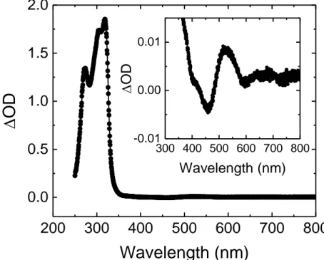
The photoswitching dynamics of the three thin films were investigated by femtosecond pump-probe optical spectroscopic measurements in transmission geometry with the experimental setup described in detail in ref. [19]. Thin films were excited with an 80-fs pump laser pulse and their transient optical transmission was probed using a delayed laser pulse. The delay between pump and probe pulses was controlled by combining a mechanical translation stage, to adjust the optical path difference for sub-ns measurements, with an electronic synchronization scheme of laser amplifiers for measurements in the ns-to-ms time domain. The film temperature was controlled in situ by a nitrogen gas flow. The experiments were carried out with a 500 Hz pump repetition rate, set to 570 nm on the weak d-d absorption band of the complex in its LS state. This absorption band centered around 535 nm is well evidenced on a thicker (700 nm) film of (1) (see Figure S1 in the Supporting Information). The laser beam of diameter ca. 150 µm propagates normal to the film surface. The pump energy was varied between 1 and 8 µJ. The probe wavelength was set to 320 nm (where the optical density change is maximum between the LS and HS states) to monitor the resulting LS-to-HS switching
dynamics through the time variation of the optical density ∆OD(t). The time evolution of the HS fraction ∆nHS(t) was then extracted from ∆OD(t), knowing the absolute change of OD
between the full LS and HS states measured, respectively, at 293 and 393 K: ∆𝑛𝐻𝑆(𝑡) =𝑂𝐷∆𝑂𝐷(𝑡)
𝐻𝑆−𝑂𝐷𝐿𝑆 (1)
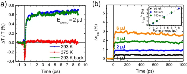
Figure 2a displays the time evolution of the relative change of the optical transmission ∆T / T
at = 320 nm in the 100-nm-thick film on the ps timescale at two different temperatures (293 and 375 K) following a 2-µJ femtosecond laser excitation. At room temperature, the induced signal reflects a decrease of the optical density, which is attributed to the photo-conversion of a small amount of molecules from the LS to the HS state. A comparative measurement performed on the same area of the film above the transition temperature (375 K) shows no detectable long-lived induced signal. Finally, the same fraction of photo-switched molecules is retrieved on return to room temperature. Comparable observations were made in the three films (see Figure S2).
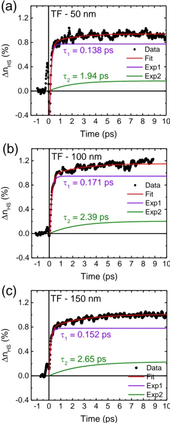
As depicted in Figure 2a, the photo-induced switching between the molecular LS and HS states, probed through the relative change of the optical transmission, typically occurs on the sub-picosecond timescale. A biexponential fit appears necessary to reproduce the observed dynamics (see Figure S3). The shorter time constant (τ1 = 171 ± 8 fs) is related to the ultrafast
dynamics of the intersystem crossing trajectory through transient excited states, that leads to the population of the HS state. Such an ultra-fast process, which takes place at the molecular scale, has been already observed in various SCO compounds, whether the switchable molecules are in solution or in a crystalline structure.[31–37] The second (longer) time constant (τ2 = 2.4 ±
0.4 ps) presumably describes the vibrational cooling of the “hot” excited molecules, which arrive in the final HS potential with excess vibrational energy.[21,38] This cooling process drains the population to the bottom of the HS potential and causes an additional slight variation of the optical density. After about ten picoseconds, the vibrational cooling is completed and the
change of optical density can be directly related to the fraction of photo-converted HS molecules. Figure 2b shows that this HS fraction, hereafter denoted ∆nHShν, remains constant
during the first nanosecond. As displayed in the inset of Figure 2b, ∆nHShν grows linearly with
the excitation density, independently of the film thickness, as expected for an intramolecular process.
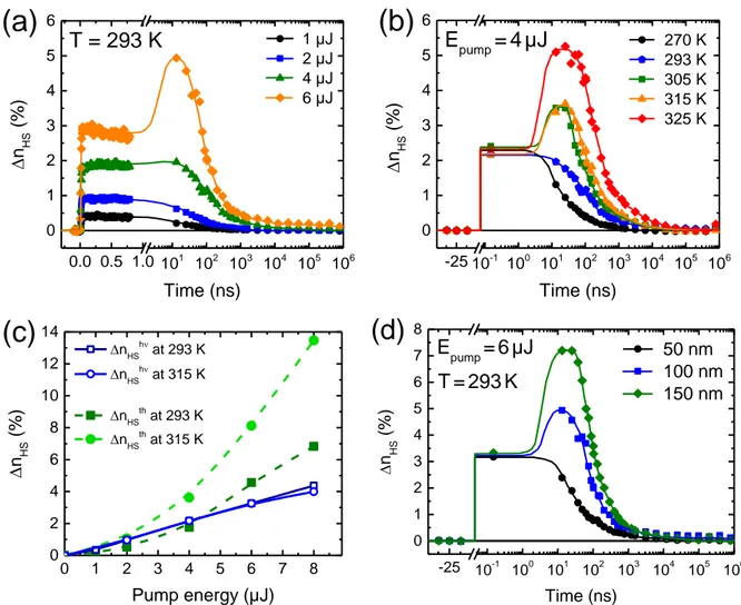
To probe the switching dynamics and the relaxation phenomena on longer timescales, we have performed measurements on a broader temporal range [100 ps – 1 ms] after photoexcitation. As depicted in Figure 3a, different photoresponses are evidenced at room temperature in the 100-nm-thick film within the ns-µs time domain depending on the excitation density. For fluences below 4 µJ, the photo-switched molecules return to the LS ground state through a single-step relaxation process occurring within 100 ns. Above a threshold excitation density (6 µJ), a pronounced increase of the fraction of HS molecules is observed in the 20–40 ns time window, which in turn leads to delaying noticeably the relaxation to the LS state. This two-step response in terms of ∆nHS has also been evidenced in the 150-nm-thick film at a lower threshold
of 4 µJ, but does not appear in the thinner film of 50 nm, at least within the explored excitation energies (see Figure S4).
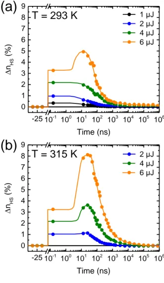
To determine the origin of this additional switching process occurring on the ns timescale, we have carried out temperature-dependent measurements. Figure 3b shows that for a given excitation density (4 µJ), the 25-ns peak grows progressively as the film temperature is increased while the sub-ns-timescale plateau remains constant (∆nHShν ≈ 2.25 %). The
temperature dependence of ∆nHS at t = 25 ns and its non-linear variation with the pump energy
(threshold effect) demonstrate that the photo-response around t = 25 ns can be related to a thermally activated switching process (this will be hereafter denoted ∆nHSth). Figure 3c
compares the variations of ∆nHShν and ∆nHSth with increasing excitation energy at two different
temperatures (see also Figure S5). As discussed above, ∆nHShν, measured on the picosecond
energy. By contrast, ∆nHSth shows a strong dependence with the temperature and its evolution
with the pump energy clearly departs from the linear regime. This non-linear behavior leads to a strong increase of ∆nHS (up to 14 %) at large excitation energies (8 µJ) and high temperatures
(315 K) in the 100-nm-thick film. At room temperature, for excitations below ca. 4 µJ, the system relaxes and ∆nHSth < ∆nHShν, whereas above this ‘threshold’ energy value, amplification
occurs and ∆nHSth > ∆nHShν. At 315 K, ∆nHSth is always higher than ∆nHShν, even when using low
pump energies.
Figure 3d compares the room-temperature photoresponse of the three films of (1) following a
6-µJ laser pulse. (The photoresponse to various excitation energies is shown in Figure S6.) As already mentioned above, the fraction of photoswitched molecules on the sub-ns-timescale plateau ∆nHShν is identical in the three films for a given excitation energy, since the pump laser
penetration depth ( ≈ 50 µm) is much larger than the thickness of the films. Size reduction effects are, however, clearly visible in the long-timescale dynamics. The main observation is that the additional switching step around 25 ns vanishes progressively when the film thickness is reduced. In the thinnest film (50 nm), regardless of the pump energy (0–6 µJ), the system directly recovers the LS ground state within ca. 100 ns. This relaxation time tends towards the molecular relaxation limit measured for similar FeII SCO systems in solution, in which the
lifetime of the photo-induced HS state falls in the typical 1–50 ns range at room temperature.[39] In the thicker films (100 and 150 nm), an additional amplification occurs (∆nHSth > ∆nHShν) and
the recovery of the thermodynamic equilibrium appears noticeably delayed towards the μs timescale.
The physical picture hinges on the following lines.
(1) In contrast with a bulk crystal, the optical pump pulse excites the SCO molecules in a homogeneous manner along the direction of the laser propagation, owing to the small thickness of the films (L ≈ 100 nm) compared to the laser penetration depth ( ≈ 50 µm at 570 nm). This
homogeneous distribution of photo-excited HS molecules within the LS lattice is clearly supported by the sub-ns experimental data in Figures 2b and 3d, which displays no thickness dependence. During the initial LS-to-HS switching step, the swelling of the molecular volume gives rise to a substantial photo-induced stress within the material. The latter is also accompanied by a thermal stress, arising from the homogeneous increase of the lattice temperature (within a few picoseconds[40]) due to the incoherent transfer of the electronic excess
energy to the lattice via electron-phonon coupling.
(2) This thermal and non-thermal photo-induced stress builds up faster than the lattice can expand, so that the macroscopic volume remains constant at this stage. The mechanical equilibrium with the environment is then restored via the coherent propagation of collective strain waves within the sample,[17,19,41] on the so-called “acoustic timescale” defined by the ratio
L / v, where L is a typical length and v is the longitudinal sound velocity (ca. 3 km.s-1).[42] Therefore, we can estimate that the photo-induced stress along the direction perpendicular to the substrate plane should rapidly relax (within only a few tens of ps), making a clear difference between thin films and bulk crystals. A sizeable expansion of the crystal lattice along the c-axis is then expected from the thermal variation of the unit-cell parameters (see Figure S7).[27] In addition, it is worth to mention that a second acoustic timescale should be considered, determined by the size of the irradiated area on the thin-film sample (beamwaist ca. 150 µm) and expected to occur on a 10’s of ns timescale.
(3) On the shortest acoustic timescale (tens of ps), despite the rise of the lattice temperature and the completion of lattice expansion along the c-axis, our experimental data do not show any additional spin-state switching. This result stems from the fact that the activated LS ↔ HS switching rate is governed by a significant intramolecular energy barrier, making the molecular spin states (LS or HS) locally “frozen” on the sub-ns timescale. Instead, the second jump of the HS fraction is observed only in the 20–40 ns range after the laser pulse. For low pump energies,
we can notice that the photoswitched HS molecules directly relax towards the thermal equilibrium state within a few tens of ns, which gives a reliable estimation of the timescale of the thermally activated molecular switching phenomenon. For higher pump energies, the observed second jump occurs within the same timescale window, which hints at the role played by thermal activation in the process. It is also interesting to mention that the observed values of
∆nHSth are in agreement with a moderate increase of the lattice temperature, which can be
estimated of the order of 3 K per % of ∆nHShν. That said, we must mention the possible role
played by in-plane elastic stress relaxation in this second switching step. Indeed, as discussed above, the in-plane relaxation can be estimated to occur on a tens of ns timescale, which is an intriguing coincidence with the delayed increase of the HS fraction.
(4) Finally, the recovery to a complete thermal equilibrium with the external environment is mainly governed by the transfer of the thermal energy, imparted by the laser pulse, into the substrate. To estimate the related timescale, we can mention that the characteristic time associated with heat diffusion across the thin films of thickness L can be approximated by the ratio τ = L2 / D
T ≈ 10–80 ns, where DT = 2.6 × 10⁻⁷ m2.s-1 is the thermal diffusivity.[28] The actual
heat transfer may require longer time at grain boundaries and/or at the film-substrate interface,[43] but will be completed in less than 1 µs.[44] This is in good agreement with our
experimental observations for the recovery of the initial state within 0.1–1 µs (depending on the experimental conditions). In the absence of heat exchange with the external environment, the same transient temperature jump (i.e. the same response in terms of ∆nHS) would be expected
in the three films. The large difference observed between the three samples proves that the reduction of the film thickness, and thereby the thermal exchange coupling with the substrate, plays a key role in the observed phenomena. Indeed, as the contribution of heat exchange follows the surface-to-volume ratio (and then varies as L-1), the reduction of the film thickness allows a better dissipation of the heat generated by the laser pulse. Consequently, size reduction
contributes to lower the transient temperature jump undergone by the sample and thus accelerate the recovery of the thermodynamic equilibrium state.
To summarize, time-resolved optical spectroscopic measurements of the out-of-equilibrium switching dynamics induced by a femtosecond laser excitation were performed on nanocrystalline SCO thin films exhibiting first-order spin transition near room temperature. The well-controlled, nanometric thickness of the studied films allowed for quantitative measurements of the transient optical transmission and an accurate determination of the photo-induced HS fraction evolving on successive timescales. Contrary to bulk samples, an important asset of the present experiments is the homogeneous distribution of the photo-switched molecules and of the lattice temperature following the laser pulse. Crucially, these high-quality, thin films brought into light the consequences of delayed thermal activation and size reduction effects on the multiscale switching dynamics. Overall, the following new features have been evidenced:
(1) The absence of spin-state switching concomitant with the lattice expansion along the direction perpendicular to the film, presumably because the corresponding acoustic timescale in such nanometric films is too short compared to the time needed to activate the molecular switching above the energy barrier, making the latter a temporal bottleneck for the transition. (2) The observation of a delayed, nonlinear, thermally activated response on the 20–40 ns timescale, governed by the intramolecular LS ↔ HS energy barrier. Further investigations are required to better understand if this additional switching step is purely of thermal origin or related to elastic contributions, as it may be suggested because the involved timescale is compatible with the in-plane strain propagation.
(3) The existence of another visible size reduction effect in the photoswitching dynamics related to a more efficient heat transfer to the substrate in the thinnest film, which has the effect of preventing the second switching step and accelerating the recovery of thermal equilibrium.
To conclude, we demonstrate that these newly synthesized high-quality SCO thin films pave the way for pioneering investigations on the switching dynamics at the nanometric scale, which are fundamental in order to control and manipulate the physical properties of SCO nanomaterials using ultrafast stimuli. Importantly, these films also offer an unprecedented opportunity to perform time-resolved diffraction studies of the structural dynamics in the near future. In terms of applications, while the sub-picosecond molecular photoswitching constitutes a well-known and appealing feature, the time needed by the system to recover its initial state has been less considered up to now, despite this being the main limiting factor for operation at high frequencies. In this context, the present results demonstrate that nanometric films of (1) can be used in ambient conditions as fast molecular switches in devices, driven by ultra-short laser excitations and working in the 1–10 MHz frequency range. Material engineering in terms of intramolecular energy barriers and thermal/mechanical couplings between the film and the substrate appear as the most promising ways for further improving/tuning the photoswitching properties of SCO nanomaterials.
Supporting Information
Supporting Information is available from the Wiley Online Library or from the author.
Acknowledgements
This work was supported by the European Commission through the SPINSWITCH project (H2020-MSCA-RISE-2016, Grant Agreement No. 734322) and by the Agence Nationale de la Recherche through the ELASTICA project (ANR-16-CE30-0018). The grants of AB and VS were financed by the Région Occitanie (contract No. 15050123) and the CNRS (Emergence project), respectively.
Received: ((will be filled in by the editorial staff)) Revised: ((will be filled in by the editorial staff)) Published online: ((will be filled in by the editorial staff))
References
[2] P. Gütlich, H. A. Goodwin, Eds., Spin Crossover in Transition Metal Compounds I-III, Springer Berlin Heidelberg, 2004.
[3] A. Bousseksou, G. Molnár, L. Salmon, W. Nicolazzi, Chem. Soc. Rev. 2011, 40, 3313. [4] M. A. Halcrow, Ed., Spin-Crossover Materials: Properties and Applications, John
Wiley & Sons, Ltd., 2013.
[5] A. Bousseksou, Ed., C. R. Chim. 2018, 21, 1055. [6] P. Guionneau, Dalton Trans. 2014, 43, 382.
[7] S. Cobo, G. Molnár, J. A. Real, A. Bousseksou, Angew. Chem. Int. Ed. 2006, 45, 5786. [8] E. Coronado, J. R. Galán-Mascarós, M. Monrabal-Capilla, J. García-Martínez, P.
Pardo-Ibáñez, Adv. Mater. 2007, 19, 1359.
[9] F. Volatron, L. Catala, E. Rivière, A. Gloter, O. Stéphan, T. Mallah, Inorg. Chem. 2008,
47, 6584.
[10] S. Shi, G. Schmerber, J. Arabski, J.-B. Beaufrand, D. J. Kim, S. Boukari, M. Bowen, N. T. Kemp, N. Viart, G. Rogez, E. Beaurepaire, H. Aubriet, J. Petersen, C. Becker, D. Ruch, Appl. Phys. Lett. 2009, 95, 043303.
[11] H. Naggert, A. Bannwarth, S. Chemnitz, T. von Hofe, E. Quandt, F. Tuczek, Dalton
Trans. 2011, 40, 6364.
[12] C. R. Gros, M. K. Peprah, B. D. Hosterman, T. V. Brinzari, P. A. Quintero, M. Sendova, M. W. Meisel, D. R. Talham, J. Am. Chem. Soc. 2014, 136, 9846.
[13] T. Mallah, M. Cavallini, C. R. Chim. 2018, 21, 1270.
[14] L. Poggini, M. Milek, G. Londi, A. Naim, G. Poneti, L. Squillantini, A. Magnani, F. Totti, P. Rosa, M. M. Khusniyarov, M. Mannini, Mater. Horiz. 2018, 5, 506.
[15] K. Senthil Kumar, M. Ruben, Coord. Chem. Rev. 2017, 346, 176.
[16] G. Molnár, S. Rat, L. Salmon, W. Nicolazzi, A. Bousseksou, Adv. Mater. 2018, 30, 17003862.
[17] M. Lorenc, J. Hébert, N. Moisan, E. Trzop, M. Servol, M. Buron-Le Cointe, H. Cailleau, M. L. Boillot, E. Pontecorvo, M. Wulff, S. Koshihara, E. Collet, Phys. Rev. Lett. 2009,
103, 028301.
[18] H. Cailleau, M. Lorenc, L. Guérin, M. Servol, E. Collet, M. Buron-Le Cointe, Acta
Crystallogr. Sect. A 2010, 66, 189.
[19] M. Lorenc, C. Balde, W. Kaszub, A. Tissot, N. Moisan, M. Servol, M. Buron-Le Cointe, H. Cailleau, P. Chasle, P. Czarnecki, M. L. Boillot, E. Collet, Phys. Rev. B 2012, 85, 054302.
[20] R. Bertoni, M. Lorenc, H. Cailleau, A. Tissot, J. Laisney, M.-L. Boillot, L. Stoleriu, A. Stancu, C. Enachescu, E. Collet, Nat. Mater. 2016, 15, 606.
[21] R. Bertoni, M. Lorenc, A. Tissot, M. Servol, M.-L. Boillot, E. Collet, Angew. Chem. Int.
Ed. 2012, 51, 7485.
[22] G. Gallé, C. Etrillard, J. Degert, F. Guillaume, J.-F. Létard, E. Freysz, Appl. Phys. Lett.
2013, 102, 063302.
[23] D. M. Sagar, F. G. Baddour, P. Konold, J. Ullom, D. A. Ruddy, J. C. Johnson, R. Jimenez, J. Phys. Chem. Lett. 2016, 7, 148.
[24] Y. Jiang, L. C. Liu, H. M. Müller-Werkmeister, C. Lu, D. Zhang, R. L. Field, A.
Sarracini, G. Moriena, E. Collet, R. J. D. Miller, Angew. Chem. Int. Ed. 2017, 56, 7130. [25] R. M. van der Veen, O.-H. Kwon, A. Tissot, A. Hauser, A. H. Zewail, Nat. Chem. 2013,
5, 395.
[26] S. T. Park, R. M. van der Veen, Struct. Dyn. 2017, 4, 044028.
[27] S. Rat, K. Ridier, L. Vendier, G. Molnár, L. Salmon, A. Bousseksou, CrystEngComm
2017, 19, 3271.
[28] K. Ridier, S. Rat, H. J. Shepherd, L. Salmon, W. Nicolazzi, G. Molnár, A. Bousseksou,
[29] V. Shalabaeva, S. Rat, M. D. Manrique-Juarez, A.-C. Bas, L. Vendier, L. Salmon, G. Molnár, A. Bousseksou, J. Mater. Chem. C 2017, 5, 4419.
[30] V. Shalabaeva, M. Mikolasek, M. D. Manrique-Juarez, A.-C. Bas, S. Rat, L. Salmon, W. Nicolazzi, G. Molnár, A. Bousseksou, J. Phys. Chem. C 2017, 121, 25617.
[31] J. K. McCusker, K. N. Walda, R. C. Dunn, J. D. Simon, D. Magde, D. N. Hendrickson,
J. Am. Chem. Soc. 1992, 114, 6919.
[32] J. K. McCusker, K. N. Walda, R. C. Dunn, J. D. Simon, D. Magde, D. N. Hendrickson,
J. Am. Chem. Soc. 1993, 115, 298.
[33] C. Bressler, C. Milne, V.-T. Pham, A. ElNahhas, R. M. van der Veen, W. Gawelda, S. Johnson, P. Beaud, D. Grolimund, M. Kaiser, C. N. Borca, G. Ingold, R. Abela, M. Chergui, Science 2009, 323, 489.
[34] A. Cannizzo, C. J. Milne, C. Consani, W. Gawelda, C. Bressler, F. van Mourik, M. Chergui, Coord. Chem. Rev. 2010, 254, 2677.
[35] M. Cammarata, R. Bertoni, M. Lorenc, H. Cailleau, S. Di Matteo, C. Mauriac, S. F. Matar, H. Lemke, M. Chollet, S. Ravy, C. Laulhé, J.-F. Létard, E. Collet, Phys. Rev.
Lett. 2014, 113, 227402.
[36] N. Huse, H. Cho, K. Hong, L. Jamula, F. M. F. de Groot, T. K. Kim, J. K. McCusker, R. W. Schoenlein, J. Phys. Chem. Lett. 2011, 2, 880.
[37] G. Auböck, M. Chergui, Nat. Chem. 2015, 7, 629.
[38] E. A. Juban, J. K. McCusker, J. Am. Chem. Soc. 2005, 127, 6857.
[39] C. Brady, J. J. McGarvey, J. K. McCusker, H. Toftlund, D. N. Hendrickson, Spin
Crossover in Transition Metal Compounds III, Springer Berlin Heidelberg, 2004, 1–22.
[40] J. Li, R. Clinite, X. Wang, J. Cao, Phys. Rev. B 2009, 80, 014304.
[41] D. Schick, M. Herzog, A. Bojahr, W. Leitenberger, A. Hertwig, R. Shayduk, M. Bargheer, Struct. Dyn. 2014, 1, 064501.
[42] M. Mikolasek, M. D. Manrique-Juarez, H. J. Shepherd, K. Ridier, S. Rat, V. Shalabaeva, A.-C. Bas, I. E. Collings, F. Mathieu, J. Cacheux, T. Leichle, L. Nicu, W. Nicolazzi, L. Salmon, G. Molnár, A. Bousseksou, J. Am. Chem. Soc. 2018, 140, 8970.
[43] H. A. Navirian, D. Schick, P. Gaal, W. Leitenberger, R. Shayduk, M. Bargheer, Appl.
Phys. Lett. 2014, 104, 021906.
[44] O. Kraieva, C. M. Quintero, I. Suleimanov, E. M. Hernandez, D. Lagrange, L. Salmon, W. Nicolazzi, G. Molnár, C. Bergaud, A. Bousseksou, Small 2016, 12, 6325.
Figure 1. (a) Photograph of the 100-nm-thick film of (1) deposited on a silica substrate. (b)
Atomic force microscopy (AFM) topography image of this film (image size is 10 × 10 µm2).
(c) Optical absorbance spectra of the 100-nm-thick film acquired at selected temperatures
between 293 K (LS) and 393 K (HS). Inset: optical density change ∆OD = OD293K – OD393K
in the three films as a function of the wavelength. (d) Temperature dependence of the HS fraction extracted from the variation of the optical density at = 317 nm along one heating-cooling cycle at 1 K / min scan rate for the three films. The inset shows the derivatives of the
200 300 400 500 600 700 800 0.2 0.4 0.6 0.8 393K O pti c al dens ity Wavelength (nm) 293K
(c)
200 400 600 800 0.0 0.2 0.4 0.6 50 nm 100 nm 150 nm OD Wavelength (nm) 300 320 340 360 380 0.0 0.2 0.4 0.6 0.8 1.0 HS phase HS frac ti on Temperature (K) 50 nm 100 nm 150 nm LS phase 330 335 340 345 0.00 0.02 0.04 0.06 0.08 dn HS /d T Temperature (K)(d)
Ra = 1.90 nm 5 mm(a)
(b)
Figure 2. Photoresponse of the thin films of (1) on the ps–ns time range to a femtosecond laser pulse. (a) Time evolution of the relative change of the optical transmission ∆T / T at
= 320 nm in the 100-nm-thick film at two different temperatures 293 K (initial LS) and 375 K (initial HS) after a 2-µJ laser pulse. (b) Time evolution of ∆nHS in the same film on the 0–
1 ns timescale at 293 K in response to a laser pulse with various excitation energies. The inset shows the evolution of ∆nHShν with respect to the laser pulse energy for the three films –
revealing the same, size-independent linear behavior. -1 0 1 2 3 4 5 6 7 8 9 10 -0.4 -0.2 0.0 0.2 0.4 0.6 0.8
(a)
Epump=2µJ T / T ( %) Time (ps) 293 K 375 K 293 K back 0 200 400 600 800 1000 0 1 2 3 4 5 1 µJ 2 µJ 4 µJ n HS (%) Time (ps) 6 µJ(b)
0 1 2 3 4 5 6 7 8 0 1 2 3 4 50 nm 100 nm 150 nm nHS h (% ) Pump energy (µJ)Figure 3. Photoresponse of the thin films of (1) on the ns-ms time range. (a) Time
evolution of ∆nHS at room temperature in the 100-nm-thick film following a femtosecond
laser pulse with various excitation energies. (b) Time evolution of ∆nHS in the same film
following an identical 4-µJ laser pulse at various temperatures between 270 and 325 K. (c) Evolution of ∆nHShν and ∆nHSth, measured respectively at 150 ps and 25 ns, with respect to
the pump energy at two different temperatures (293 and 315 K). (d) Comparative photoresponse at room temperature of the three films of (1) to a 6-µJ femtosecond laser pulse. For each plot, symbols are experimental data points and lines are drawn to guide the eye.
0.0 0.5 1.0 101 102 103 104 105 106 0 1 2 3 4 5 6
(a)
T = 293 K n HS (% ) Time (ns) 1 µJ 2 µJ 4 µJ 6 µJ -25 10-1 100 101 102 103 104 105 106 0 1 2 3 4 5 6(b)
n HS (% ) Time (ns) 270 K 293 K 305 K 315 K 325 K Epump=4µJ 0 1 2 3 4 5 6 7 8 0 2 4 6 8 10 12 14(c)
n HS (% ) Pump energy (µJ) nHSh at 293 K nHSh at 315 K nHSth at 293 K nHSth at 315 K -25 10-1 100 101 102 103 104 105 106 0 1 2 3 4 5 6 7 8(d)
n HS (%) Time (ns) 50 nm 100 nm 150 nm Epump=6µJ T=293KTable of contents
Size reduction effects have been evidenced on the room-temperature photoswitching dynamics of spin-crossover thin films induced by femtosecond laser excitations. A delayed, thermally activated switching is observed on the 20–40 ns timescale, governed by the intramolecular energy barrier between the two spin states. This additional switching step is suppressed in the thinnest films and the thermal equilibrium state is recovered within 100 ns.
Keyword:
ultrafast spin-state photoswitching
Karl Ridier, Alin-Ciprian Bas, Victoria Shalabaeva, William Nicolazzi, Lionel Salmon, Gábor Molnár,* Azzedine Bousseksou, Maciej Lorenc,* Roman Bertoni, Eric Collet, and Hervé Cailleau
Finite size effects on the switching dynamics of spin-crossover thin films photo-excited by a femtosecond laser pulse
Supporting Information
Finite size effects on the switching dynamics of spin-crossover thin films photo-excited by a femtosecond laser pulse
Karl Ridier, Alin-Ciprian Bas, Victoria Shalabaeva, William Nicolazzi, Lionel Salmon, Gábor Molnár,* Azzedine Bousseksou, Maciej Lorenc,* Roman Bertoni, Eric Collet, and Hervé Cailleau
Figure S1. Optical density change ∆OD = OD293K – OD393K measured on a 700-nm-thick film
of (1). The inset shows the weak absorption band in the visible range centered around 535 nm.
200
300
400
500
600
700
800
0.0
0.5
1.0
1.5
2.0
OD
Wavelength (nm)
300 400 500 600 700 800 -0.01 0.00 0.01 OD Wavelength (nm)Figure S2. Time evolution of the photo-induced HS fraction ∆nHS on the picosecond timescale
in the three films (a) 50 nm, (b) 100 nm and (c) 150 nm, and at two different temperatures (room temperature, initial LS state and high temperature, initial HS state) after a 2-µJ laser pulse. -1 0 1 2 3 4 5 6 7 8 9 10 -0.8 -0.4 0.0 0.4 0.8 1.2
(a)
TF - 50 nm
n HS (%) Time (ps) 298 K 375 K 298 K back -1 0 1 2 3 4 5 6 7 8 9 10 -0.8 -0.4 0.0 0.4 0.8 1.2(b)
n HS (%) Time (ps) 293 K 375 K 293 K backTF - 100 nm
-1 0 1 2 3 4 5 6 7 8 9 10 -0.8 -0.4 0.0 0.4 0.8 1.2(c)
TF - 150 nm n HS (%) Time (ps) 300 K 393 K 300 K backFigure S3. Time evolution of ∆nHS at room temperature in the three films (a) 50 nm, (b) 100
nm and (c) 150 nm. The growth kinetics of the HS fraction are described using a biexponential model. The shorter time constant (typically τ1 = 140–170 fs) is related to the ultrafast dynamics
of the intersystem crossing process between the LS and HS states and the second (longer) time constant (τ2 = 1.9–2.7 ps) describes the vibrational cooling of the “hot” excited molecules,
which populate the HS potential with an excess vibrational energy.
-1 0 1 2 3 4 5 6 7 8 9 10 -0.4 0.0 0.4 0.8 1.2 TF - 50 nm 2 = 1.94 ps n HS (% ) Time (ps) Data Fit Exp1 Exp2 1 = 0.138 ps
(a)
-1 0 1 2 3 4 5 6 7 8 9 10 -0.4 0.0 0.4 0.8 1.2(b)
TF - 100 nm 2 = 2.39 ps n HS (% ) Time (ps) Data Fit Exp1 Exp2 1 = 0.171 ps -1 0 1 2 3 4 5 6 7 8 9 10 -0.4 0.0 0.4 0.8 1.2(c)
2 = 2.65 ps n HS (% ) Time (ps) Data Fit Exp1 Exp2 1 = 0.152 ps TF - 150 nmFigure S4. Evolution of ∆nHS at room temperature on the ns-ms time window in the three films
(a) 50 nm, (b) 100 nm and (c) 150 nm, following a femtosecond laser pulse with various
excitation energies. In the thinner film (50 nm), the relaxation occurs through a one-step process regardless of the pump laser energy (0–6 µJ). In the 100-nm-thick film, a self-amplification of the fraction of HS molecules is observed around 20–40 ns above a threshold energy value of 6 µJ. The same behavior is observed in the 150-nm-thick film, but the additional switching step appears above a threshold laser energy of 4 µJ.
-25 10-1 100 101 102 103 104 105 106 0 1 2 3 4 5 6 7 8
(a)
n HS (% ) Time (ns) 1 µJ 2 µJ 4 µJ 6 µJ TF - 50 nm -25 10-1 100 101 102 103 104 105 106 0 1 2 3 4 5 6 7 8(b)
TF - 100 nm nHS (% ) Time (ns) 1 µJ 2 µJ 4 µJ 6 µJ -25 10-1 100 101 102 103 104 105 106 0 1 2 3 4 5 6 7 8(c)
TF - 150 nm n HS (% ) Time (ns) 1 µJ 2 µJ 4 µJ 6 µJFigure S5. Time evolution of the photo-induced HS fraction in the 100-nm-thick film following
a femtosecond laser pulse with various excitation energies at two different temperatures: (a) 293 K and (b) 315 K. For the same used excitation energies, the second jump of the HS fraction at 25 ns, ∆nHSth, appears noticeably more pronounced at 315 K (i.e. 22 K below the transition
temperature), indicating that this additional switching step occurs through a thermally activated process. -25 10-1 100 101 102 103 104 105 106 0 1 2 3 4 5 6 7 8 9
(a)
n HS (% ) Time (ns) 1 µJ 2 µJ 4 µJ 6 µJT = 293 K
-25 10-1 100 101 102 103 104 105 106 0 1 2 3 4 5 6 7 8 9(b)
T = 315 K
n HS (% ) Time (ns) 2 µJ 4 µJ 6 µJFigure S6. Comparative photoresponse at room temperature of the three films of (1) to a
femtosecond laser pulse with various excitation energies: (a) 2 µJ, (b) 4 µJ and (c) 6 µJ.
-25 10-1 100 101 102 103 104 105 106 0 1 2 3 4 5 6 7 8
(a)
Epump = 2 µJ n HS (%) Time (ns) 50 nm 100 nm 150 nm -25 10-1 100 101 102 103 104 105 106 0 1 2 3 4 5 6 7 8(b)
Epump = 4 µJ n HS (%) Time (ns) 50 nm 100 nm 150 nm -25 10-1 100 101 102 103 104 105 106 0 1 2 3 4 5 6 7 8(c)
Epump = 6 µJ n HS (%) Time (ns) 50 nm 100 nm 150 nmFigure S7. Thermal variation of the unit-cell parameters and lattice volume extracted from
X-ray diffraction measurements on a bulk powder sample of (1) in the heating mode.[S1]
Reference
[S1] S. Rat, K. Ridier, L. Vendier, G. Molnár, L. Salmon, A. Bousseksou, CrystEngComm 2017, 19, 3271.