HAL Id: hal-03015412
https://hal.archives-ouvertes.fr/hal-03015412
Submitted on 4 Dec 2020HAL is a multi-disciplinary open access
archive for the deposit and dissemination of sci-entific research documents, whether they are pub-lished or not. The documents may come from teaching and research institutions in France or abroad, or from public or private research centers.
L’archive ouverte pluridisciplinaire HAL, est destinée au dépôt et à la diffusion de documents scientifiques de niveau recherche, publiés ou non, émanant des établissements d’enseignement et de recherche français ou étrangers, des laboratoires publics ou privés.
alloys
Adrien Bourgine, Jérémie Grisolia, Maxime Vallet, Daniel Benoit, Y. Le Friec,
V. Caubet-Hilloutou, Alain Claverie
To cite this version:
Adrien Bourgine, Jérémie Grisolia, Maxime Vallet, Daniel Benoit, Y. Le Friec, et al.. On the charge transport mechanisms in Ge-rich GeSbTe alloys. Solid-State Electronics, Elsevier, 2020, 172, pp.107871. �10.1016/j.sse.2020.107871�. �hal-03015412�
1
On the charge transport mechanisms
in Ge-rich
GeSbTe alloys
Adrien Bourgine1, Jérémie Grisolia1, Maxime Vallet2, Daniel Benoit3, Y. Le Friec3, V.
Caubet-Hilloutou3 and Alain Claverie2
1 Laboratoire de Physique et Chimie des Nano Objets (LPCNO), INSA, Toulouse, France 2 CEMES-CNRS, Toulouse, France
3 STMicroelectronics, Crolles, France
Corresponding author : jéré[email protected]
Abstract:
Ge-rich GeSbTe (GST) alloys are attracting Phase Change Materials for future memories as their higher crystallization temperature offers an extended range of applications. We have studied the electrical characteristics of PCM cells using such alloys as active layers. We show by impedance spectroscopy that the cells in the RESET (amorphous) state are not only resistive but also exhibit a capacitive component. Although trap-assisted conduction models are apparently able to describe the I(V) and I(T) characteristics of the devices in this state, their physical background is thus questionable. Alternatively, we show that granular models, describing electrical transport through conductive grains separated by insulating interfaces, are also able to simulate these characteristics, while fed by physically sound fitting parameters. Moreover, we show that the SET (crystalline) state is not simply ohmic but that its characteristics, as conductive as a metal but reacting as an insulator to temperature, resemble to those found in a semiconductor doped with a very low ionization energy defect. Finally, all these characteristics can be understood by considering that the electrical properties of cells made of Ge-rich GST layers are not those characteristic of some defective and homogeneous material but instead result from strong chemical heterogeneities found both in the amorphous and crystalline states of these Ge-rich alloys.
Keywords: phase change memory; GeSbTe alloys; electron transport; impedance spectroscopy; characterization; modeling.
Highlights:
- RESET state of Ge-rich GST is not only resistive but also shows a capacitive component.
- Granular models for heterogeneous materials as good as trap-assisted models to simulate I(V) and I(T) curves. Physically more relevant.
- SET state is not simply ohmic. Characteristics resemble those of a doped semiconductor.
- Overall characteristics assigned to chemical and phases heterogeneities. In relation with the tendency of the Ge-rich alloys to decompose in pure Ge and GST phases.
2
Introduction
Phase Change Materials (PCMs) are again attracting the interest of microelectronic industries as they are foreseen to be exploited as active materials within the next generation of electronic memories [1
-4]. PCMs may be found in two phases, amorphous or crystalline, which can be changed by means of heating processes [2]. In Phase Change Random Access Memories (PCRAMs), the information bits 0/1 are stored in the high resistive amorphous state and in the low resistive crystalline state, respectively, while phase switching is induced by means of electrical pulses through Joule heating [1]. Prototypical PCMs are made of GeTe and GeSbTe alloys [5] which have been extensively studied for their rapid switching speed (time scale up to nanosecond [6] and sub-nanosecond [7]) and high resistivity contrast between the amorphous and crystalline phases (up to 104 ohm·cm [8, 9]). From a technological viewpoint, PCRAMs are attracting due to their cyclability [10], endurance [4] and fast programming [11], while providing an extremely easy scaling path [4]. Another important property of a PCM is its crystallization temperature (Tχ), which dictates the stability of the amorphous phase and the reliability of the PCRAM when exposed to high working temperatures [12, 13]. The canonical GeTe and Ge2Sb2Te5 materials have relatively low Tχ, what significantly restricts their field of applications. The quest for PCMs having higher Tχ for specific embedded applications has triggered the discovery of Ge-rich Ge-Sb-Te (GST) alloys, where the Tχ is found to increase with the Ge content [14], [15]. This paper intends to contribute to the exploration of the electrical characteristics and properties of these technologically important materials.
Surprisingly, after decades of research, the origin of the electrical behavior of GST alloys remains under debate. Many questions are still unanswered. Among them, the nature of the current during the phase switching process, or more surprisingly, the conduction modes allowing carrier transport through the material. Electrical conduction within the amorphous phase (commonly referred as the RESET state) is often explained via the thermal emission and assisted tunneling of carriers via interacting traps (Poole model) or non-interacting traps (Poole-Frenkel model). These models are inherited from the semiconductors background and were originally introduced to explain conduction within amorphous oxides, such as SiO2. Through the years other plausible mechanisms have been suggested to explain the non-linear behavior of the current in the RESET state: variable range hopping [16], percolation process [17, 18], or space charge limited current [19] to cite few.
Still discussions on that matter are ongoing; the difficulty to bring and find consensus on a definitive framework comes from the fact that the physical laws governing these different conduction modes write mathematically quite the same [20, 23]. For this reason, almost every conduction mode can be found to satisfactory fit some limited set of data, although they often rely on different, contradictory, physical explanations. Adding that these different mechanisms can possibly compete over wide ranges of voltages and temperatures [23, 24], one understands the difficulty to conclude. The identification of a possible conduction mode should not only rely on the ability of a formula to fit a limited set of experimental data but also on the physical meaning of the parameters extracted from the fit [25]. The ubiquity of the Poole-Frenkel effect, which is quite systematically designed to be at the origin of the main conduction modes observed in thin oxide films, has been pointed out by H. Schroeder who has highlighted the very narrow range of experimental conditions in which such a conduction mode is expected to arise [26].
The present paper aims at investigating and discussing the characteristics of charge transport in Ge-rich GST layers in the RESET and SET states and at questioning the relevance of the Poole-Frenkel effect and trap-limited models to describe conduction mechanisms in such alloys. We evidence by impedance spectroscopy that the RESET (amorphous) state shows a capacitive component not expected in an homogeneous semiconductor. We show that models either describing trap-limited conduction in a semiconductor or conduction in a granular medium can fit the data but that the significance and the values of the physical parameters which are extracted from the fits deserve discussion. We have also investigated the electrical behavior and characteristics of the SET state which has been barely studied in the past. While GST alloys in the crystalline SET state are often considered as metals showing “simply ohmic” behavior,
3
we show that Ge-rich GST alloys are indeed purely resistive but also show non-linear characteristics at relatively low voltages.
1. Critical literature survey
1.1 Conduction in the amorphous (RESET) state
Nowadays, the trap-limited conduction model, as proposed by Ielmini & al. [27], is largely accepted by the scientific community and also used for the design of industrial memories [29]. This model currently works well. It proposes an apparently coherent physical picture and well explains the measured variations of the activation energy of the transport mechanism as a function of the applied voltage. The original paper written by Frenkel [30] from which it is derived was aimed at giving a description of conduction in insulators and semiconductors. The “Poole-Frenkel” effect was introduced to explain the deviations of the (non-linear) current-voltage experimentally obtained data from the predictions of the Poole model [31]. Since then, charge transport in amorphous materials has traditionally been described via the presence of traps within the materials [31]. This phenomenon gives rise to conduction through the thermal emission or tunneling (or both) of carriers between these traps. Although the landscape of charge transport theories in amorphous materials is very rich, the Poole-Frenkel (PF) model gradually took over and became the most widely used. Besides Schroeder [26], other authors have warned the community on the questionable hegemony of the PF model in the field of microelectronics [26]. From the point of view of Physics, the Poole-Frenkel effect is ideally suited to describe the non-linear response to voltage of crystalline semiconductors, as the defects are known to be coulombian in such materials. In amorphous solids, conduction results also from disorder effects, probably more that from trap conduction [19], and this renders the applicability of this model rather questionable. Nonetheless, GST was no exception and today conduction in amorphous GST is usually described through some “enhanced Poole-Frenkel effects” (still is a matter of debate for theorists), giving rise to a vast family of context-specific physical laws [23, 24, 27, 28]. However, as far as Ge-rich GST alloys are concerned and as it will be shown later, the results we have obtained by spectroscopic analysis do not match with the application field of the PF model.
Impedance analysis of the SET and RESET states in GST-based PCM cells have already been used to measure the dielectric constant of the material and try to infer the possible conduction modes they can sustain [33]. In the literature, two types of electrical equivalent circuits have been proposed for GST, a “one-RC” model [33] and a “two-“one-RC” model [34]. These characteristics suggest the presence of grains of different conductivities and able to store charges both within the polycrystalline and amorphous materials. However, as the SET state is very often found conductive, as expected for a metal, the previously reported presence of a capacitance in the equivalent circuit is quite surprising. We will show that our results do not confirm this finding, at least for the Ge-rich GST alloys.
Moreover, activation energies are quite often calculated, mainly because they are easy-to-get “physical” values, to have an idea about and start discussion. One can always define some energy of “activation” as the amount of energy necessary for one carrier to take part to some conduction mechanism. It is comfortably independent of the theoretical framework used for the analysis and can be discussed at length. Beyond the “value”, papers rarely exploit this quantity and discuss the physical framework leading to its determination. Nardone et al. recommend the value of 0.37 eV for PCM in the RESET state under low bias but with fluctuations from 0.3 eV to 1 eV [20]. This energy of activation is half the value of the band gap, under the hypothesis that a band structure theory is valid for amorphous GST. In this paper, we will try to discuss the physics of this energy of activation, rather than focusing only on its numerical value.
Oddly, the structure and exact composition of the GST alloys under study are not always taken into account to interpret and discuss the conduction modes. It is known that multiple cycling of the devices leads to chemical segregation even for the canonical 225 GST [22]. Moreover, the need for devices working at higher temperatures has led to the exploration of fairly exotic GST alloys both in terms of compositions [33] and in terms of doping [34, 37]. Quite often, the initial composition of the alloys is overlooked. Nevertheless, a common feature of GST – and all ternary alloys – is that compositions that do not stand on the congruent
4
pseudo-line will decompose into stable phases during thermal cycling. Whether or not the material is homogeneous is absolutely crucial to interpret the data. For this reason, in our work, we compare the results obtained on two Ge-rich GST materials of different Ge contents, keeping in mind their different chemical compositions and the non-homogeneities they contain [21], [35].
1.2 Conduction in the (poly)-crystalline (SET) state
The conduction modes of GST alloys in the polycrystalline (SET) state have not received so much attention in the past. It is generally assumed that the SET state is typical of a metal and shows almost ohmic I(V) characteristics. Two papers have reported a possible metal-insulator transition at low temperature [38, 39]. Moreover, impedance spectroscopy has been used to investigate the structural transition between the RESET and the SET states. In the case of GST-225, the polycrystalline (SET) phase was described by a RC model using smaller resistances than those needed to describe the amorphous (RESET) state [34]. However, we will see later in this paper that, in contrast, our impedance spectroscopy results on Ge-rich alloys do not reveal any capacitance contribution to this SET state.
2. Materials and methods
In this work, two different GST compositions were studied. They are both Ge-rich and relatively remote from the canonical 225 composition ([Ge]>30%). They will be referred as alloy A and B in the following, alloy B being richer in Ge than alloy A. They were both embedded in wall-shape PCM structures [35] contacted via two copper pads connected to the electrodes, as schematically drawn in Figure ESI 1.
Dynamic tests and initializations were performed beforehand to ensure the well-functioning of the cells. They are detailed in Figure ESI 2, Figure ESI 3 and Figure ESI 4. Forming steps were achieved via repetitions of RESET and SET pulses until fully functioning PCM cells were obtained. This process is similar to the R-V curves method (Figure ESI 4).
Most electrical characterizations were performed under DC voltage using a Keithley 4200-SCS DC characterization system and a cryogenic probe station (Janis ST-500-1) operating at 10-5 mbar in the temperature range 77-300 K. Temperature control was achieved by using a Lakeshore 350 with a cooling/heating rate of about 2K/min. The Keithley’s 4200-SCS DC characterization system was equipped with a Keithley Source Measurement Unit (SMU) pre-amp having a resolution of approximately 1 fA with triaxial connections. I(V) measurements were performed by applying the voltage V in the form of sweeping pulses, while the current I was measured at each voltage step ∆V after a time delay ∆t, what defines an equivalent sweep rate ∆V/∆t. All measurements were performed with a sweep rate of 0.1 V/s. The measurements were carried out at different temperatures, from T = 300 K to 150 K. Enough time was left between each measurement to allow the system reaching thermal equilibrium. Temperature-dependent resistances R(T) were extracted from the slopes of the linear fits of the I(V) curves, at low voltage and for each temperature.
Impedance spectroscopywas carried out using a Keysight Impedance Analyzer EA4990A. PCM cells were tested under a sinusoidal voltage of 30 mV in amplitude, zero DC voltage bias and probed from 20 Hz to 1 MHz. All tests were performed at room temperature (T = 293K) and under dark conditions to avoid carriers injection into the wafer.
Following electrical characterization, cells were extracted and thinned down to electron transparency using a FEI Helios Nanolab 600 dual-beam FIB. TEM (Transmission Electron Microscopy) imaging and diffraction were performed using an aberration corrected FEI TECNAIF20, equipped with a FEG source.
5
3. Results
3.1 RESET state
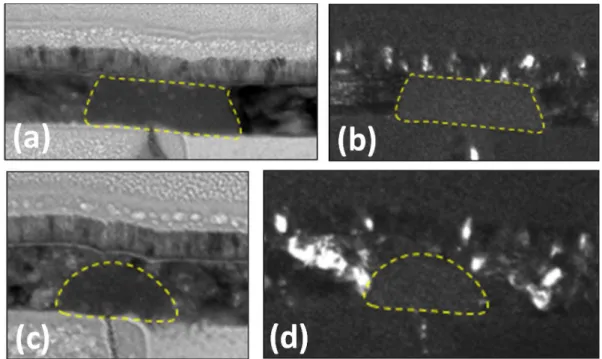
Figure 1a and 1b are bright and dark fields TEM images, respectively, of a cell made using alloy A as PCM layer after its forming step. Figure 1c and 1d shows a cell made with alloys B. Under such conditions, amorphous domes can be visualized and are highlighted with yellow dashed lines in the images.
Figure 1: TEM images of cells in the RESET state. a) and c), in bright field mode; b) and d) in dark field mode. Note that the heater in Figure 1a was degraded during FIB preparation.
Interestingly, in the cell made with alloy A, the amorphous region extends from the heater to the top electrode while in the cell made with alloy B it is somehow confined in the bottom region of the active layer. These TEM images confirm the amorphous nature of the material after forming and reaching the RESET state. However, it also demonstrates that the conduction path in a cell in the RESET state may go through an entirely amorphous material or through a stack of amorphous and crystalline layers.
Figure 2a and 2b shows the I(V) characteristics of cells A and B in the RESET state, as function of temperature. Both cells display a non-linear behavior with an ohmic domain at low fields (V < 0.2 V) and an exponential domain at higher fields. The voltage threshold separating these two domains decreases when the temperature increases. Temperature plays a dramatic role on the current output: at a fixed tension of 0.8 V, the current typically increases by a factor of ten from 150 to 300 K. We note that the sometimes observed “super exponential domain” [41], [42] is not seen here.
6
(c)
Figure 2. I(V) characteristics of the RESET states for (a), alloy A and (b), alloy B. (c), R(T) characteristics of the RESET state for alloys A and B (extracted at V=0.2V).
The resistance of the cells in the linear regime evidenced at low field (roughly for V ≤ 0.2 V) can be calculated from the ratio of the voltage by the current at a fixed temperature. Results are shown in Figure 2c. The RESET resistance of both alloys exponentially increases with decreasing temperature which is a typical feature of insulators. Charge transport is usually assumed to occur via the emission of carriers from defects into the quasi-conduction band of the material and is thus thermally activated [27]. In this framework, the exponential shape of the resistance is modulated by the activation energy of the conduction mechanism and can be analytically written as R = R0.eEa/kT ,where R0 is a pre-exponential constant and Ea is the effective (average) energy barrier for hopping. This activation energy corresponds to the energetic cost carriers have to pay in order to take part to conduction at low field.
However, as shown in Figure 2a and b, above a certain threshold voltage, the I(V) curves show a non-linear behavior. Thus, the activation energy for conduction appears to be constant at low field but depends on the applied voltage above some threshold. Indeed, Ea may contains two distinct terms, Ea = f(V)
0.0 0.2 0.4 0.6 0.8 1.0 0.01 0.1 1 10 100 1000 (b) 296K 268K 239K 208K 175K I (n A ) V (V)
7
- Φ, where Φ = EC - EF, the gap between the conduction band and the Fermi level for the amorphous material at zero electric field. f(V) is a function of voltage V whichdepends on the conduction mode. This prompted Beneventi et al. [43] to develop a new “Poole-Frenkel 3D” model to describe the behavior of the I(V) curves at all voltages through a single equation. This equation provides a good fit to experimental data at low and high fields. In this model, Ea the activation energy for conduction writes [43],
log 1
We have analyzed our data (Figure 2) following this approach. Figure 3a and b shows the variations of log(I) as a function of the variable q/kBT at fixed voltages.
©
Figure 3. I(T) characteristics of the RESET states for (a), alloy A and (b), alloy B. (c), activation energies of the conduction mechanism in the RESET state as a function of voltage (alloys A and B).
Activation energies Ea can be extracted from the slopes of the curves shown in Figure 3a and b. Results are shown in Figure 3c. This figure highlights the dramatic impact of the chemical composition of the active material over the transport mechanism. The different shapes found for the two alloys show that the conduction modes cannot be the same in the two cells despite they are both made of a Ge-rich GST. For alloy A, the energy of activation is clearly non-linear and shows the same shape than the one shown by Ielmini & al. [27]. For these authors, this behavior must be understood in the framework of Poole-Frenkel model and the observed reduction of the activation energy for increasing voltage results from the field-induced lowering of the barrier trapping the carriers on the defects. In contrast, alloy B unquestionably shows a linear dependence of the energy of activation as a function of the voltage. However, we note that Ea is not proportional to √V – Φ, as expected by the simple Poole-Frenkel model. The barrier at zero electric
0,1 1 10 100 1000 35 45 55 65 75 lo g (I ) (n A ) q/kB.T (eV-1) (a) 100mV 200mV 300mV 400mV 500mV 600mV 700mV 800mV 0,1 1 10 100 1000 35 45 55 65 lo g (I ) (n A ) q/kB.T (eV-1)
(b)
100mV 200mV 300mV 400mV 500mV 600mV 700mV 800mV 900mV 1V (c)8
field yields ~ 100 meV for alloy A and 95 meV for alloy B. Both are low values compared to those reported in literature [20, 28]. These values are more indicative of a doped than of an intrinsic semiconductor for which this barrier is of about 300 meV, i.e. half of the bandgap [28], [42].
Additional qualitative information concerning the nature of the medium through which transport takes place can be obtained via impedance spectroscopy. Figure 4a and 4b show the variations of the phase and impedance of the medium as a function of the voltage frequency. Both the phase and the impedance exponentially decrease when increasing frequency, the phase finally reaching the value of 90°. This implies that the equivalent electrical diagram of the cells must include a capacitance. This characteristic is also found in granular materials where conduction can be “easy” or “difficult” depending on the distance between the conductive elements [45].
(a) (b)
(c) (d)
Figure 4. Variations of the impedance and phase as functions of frequency in the RESET state for (a), alloy A and (b), alloy B (see also Figure ESI 5). (c), Nyquist plot of the RESET states of the two alloys and (d), equivalent circuit generating these plots.
Impedance spectroscopy has been previously used to understand charge transport [34] and phase transitions [33] in various chalcogenide glasses. In these papers, only the SET state was investigated. Given the polycrystalline nature of the material in this state, grains boundaries are believed to act as resistances to electrical transport but also to provide retention tanks (capacitive elements) for charges carriers. Thus, the cell was described by a resistance in parallel with a capacitance, which values depend on grains boundary properties. While a reasonable assumption for the SET state, it was argued that the same characteristics could not be expected for the amorphous RESET state, as the current is flowing through a continuous and homogeneous material. Interestingly, our results show that even the RESET state has a capacitive behavior. This demonstrates that the cell in the RESET state cannot consist of a chemically and structurally homogeneous material.
Figure 4c shows the Nyquist diagrams obtained for the RESET states of the two alloys. The semi-circle is characteristic of a simple cell that contains a resistance (R of grain boundary, Rgb) and a capacitance
-90 -80 -70 -60 -50 -40 -30 -20 -10 0 0 200 400 600 800 1000 0 10 20 30 40 50 P h a s e ( °) Frequency (kHz) Im p e d a n c e ( M Ω ) Impedance (MΩ) Phase (°) -90 -80 -70 -60 -50 -40 -30 -20 -10 0 0 100 200 300 400 500 0 10 20 30 40 50 P h a s e ( °) Frequency (kHz) Im p e d a n e ( M Ω ) Impedance (MΩ) Phase (°)
9
(C of grain boundary, Cgb) in parallel, along with a contact resistance [33, 34]. The extrema of the semi-circle for - Im(Z) = 0 respectively yields Rcontact and Rgb + Rcontact. The capacitance can be extracted by reading the frequency that corresponds to the topmost point of the semi-circle of the Nyquist plot and using the relation,
1 2 . [34]
From Figure 4c, we get Cgb = 8 pF and 3 pF for alloys A and B, respectively. These relatively large values cannot result from some experimental artifact since the same measurements conducted on the same cells but set in the SET state do not show any capacitive behavior, as it will be shown later in this paper. Actually, these measurements confirm that the RESET characteristics we measure cannot result from trap-assisted conduction in a semiconductor or an insulator. Alternatively, these characteristics resemble to those observed in granular media [44]. Our results finally suggest that the current passes through structural and chemical inhomogeneities, probably consisting of grains of different conductivities, within a globally amorphous and insulating matrix.
3.2 Models
There are plenty of models that can be used to describe charge transport in semiconductors and insulators. Most of them can reproduce to some extent the non-linear behavior of the current observed at high electric fields. While the selection of one of these trap-assisted models should rely for a large part on the characteristics of the material through which the current flows, this choice can be complicated if the density of states in the gap is unknown. Most models can fit any dataset, as several “free” parameters can always be adjusted. But the choice should be based on the ability of a particular model to describe the Physics of the phenomenon.
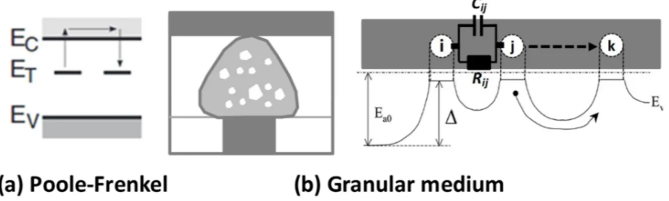
In the following, we introduce and briefly discuss two types of models we believe are relevant to discuss the electrical characteristics of amorphous Ge-rich GST alloys (Figure 7). First is the Poole-Frenkel model, mainly because of its popularity in the GST literature. It can lead to different laws depending on the trap density (Figure 6). Guided by the conclusions of our impedance analysis, we will also introduce a model suitable to describe electrical transport in a medium containing grains or inclusions in a matrix. This model also leads to two distinct laws depending on the grain density (Figure 6).
Figure 5. (a), the “classical” Poole-Frenkel (PF) model describes carrier emission from isolated traps to the
conduction band, assuming that the traps are far enough from each other so that their contribution to the potential profile can be neglected; (b) left, PCM cell with an amorphous dome (RESET state) containing conductive grains separated by some more resistive material. Right: a fragment of amorphous matrix with embedded conductive grains (i, j, k). The energy band diagram shows the valence band edge (dashed line) and the chemical potential (dot-dashed line). Ea0 is the activation energy characteristic of the insulating matrix, ∆ is the offset generated by the conductive
10
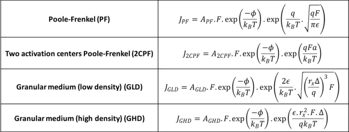
Figure 6. Expressions giving the current for the different conduction models. F = V/dPCM is the electric field, dPCM is
the distance across which the voltage drops (taken equal to the thickness of the GST active layer), Φ is the activation energy at zero field, ε = εr.ε0 the permittivity of the material, SPCMthe area of the PCM cell, a is the distance between
two coulombian traps, rx is the mean radius of the grains and ∆ is the energy offset between the grains and the
matrix. For the granular models, the band offset is taken equal to 0.4 eV and the relative permittivity is taken at 15 [53].
Poole-Frenkel and two activation centers Poole-Frenkel:
The Poole-Frenkel effect is the most often assumed conduction mode in chalcogenide materials. Historically, it was introduced by Frenkel in 1938 in an attempt to describe the log(I/V) ~ √V dependence in oxides at high fields that the Poole law was unable to explain [30]. The “classical” Poole-Frenkel (PF) model describes carrier emission from isolated traps to the conduction band and assumes that the traps are far enough from each other so that their contribution to the potential profile can be neglected (Figure 7). Charge transport non-linearity results from the lowering of the traps’ barriers by the high field. Ideally, the traps should be neutral but this is rarely the case [47]. However, when the distance between traps decreases, i.e. when the trap density is high or, alternatively, when the electrical field is high, the barrier lowering starts to linearly depend on the applied electrical field and log(I/V) shows a linear dependence to the field [52]. This behavior can be described by the “two interacting coulombian centers Poole-Frenkel” (2CPF) model for which log (I/V) ~ V (Figure 11. ) [21]. Actually, the notion of “low” or “high” defect densities depends on the applied field. Practically, for a given field, the 2CPF model is better suited to describe carrier transport in a highly defective medium [52].
Granular medium:
As suggested by impedance spectroscopy, we consider electron transport through a granular medium consisting of conductive grains dispersed in a more resistive matrix (Figure 7b). The grains can easily transport and store charges. They are separated from each other by some distance in the matrix which defines the grain boundary. In the energy diagram, a band offset appears between the matrix and the grains. This band bending in the amorphous matrix results from the redistribution of charge carriers in the continuum spectrum of localized states [53]. The carriers can hop from one grain to another when a high enough voltage is applied across the material. As the carriers are expected to move freely inside the grains, only the distance between two grains along the conduction path plays a role in the conduction. Mathematically, the relation between current and voltage resembles to that used in the Poole-Frenkel model and it is again necessary to distinguish two cases, depending on the grain density.
Poole-Frenkel (PF) . . exp !" # . exp $ # . $ % &
Two activation centers Poole-Frenkel (2CPF) 2 2 . . exp !"
# . exp
$ '
#
Granular medium (low density) (GLD) ()* ()*. . exp !"
# . exp 2% # . +,Δ $ 3 &
Granular medium (high density) (GHD) (/* (/*. . exp !"
# . exp
%. +,2. . Δ
11
Finally, Figure 6 puts together the different expressions of the current through the medium, depending on the different models used to describe electrical transport through a layer of thickness dPCM submitted to a voltage V [52].
3.3 Testing of the models:
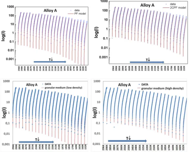
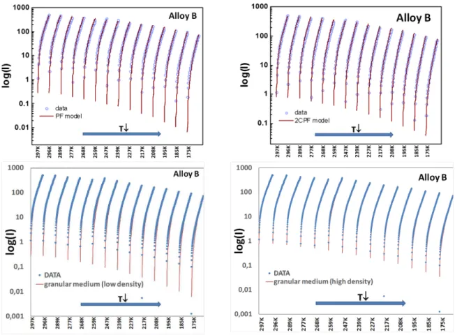
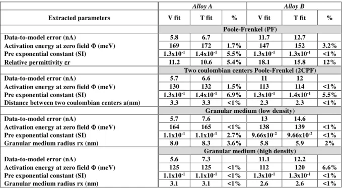
We have run a fitting procedure to reproduce the I(V) curves we have experimentally measured. The I(V) and I(T) curves were fitted independently at fixed T and V, respectively, using the relations given in Figure 6, Figure 7 and Figure 8 show the comparison of the I(V) curves we have measured at various temperatures with those predicted by the four different models for alloy A and B, respectively.
Figure 7. Variations of the log of the current as a function of the applied voltage (up to 0.8 V), for decreasing temperatures (from 296K to 152K, left to right) for Alloy A.
12
Figure 8. Variations of the log of the current as a function of the applied voltage (up to 0.8 V), for decreasing temperatures (from 297K to 175K, left to right) for Alloy B.
At first glance, all models reasonably fit the data and none can be immediately ruled out. This illustrates that the identification of a conduction mode in a resistive material cannot be simply and only based on I(V) and I(T) data. Slight deviations at high/low fields of high/low temperatures can be found for all models. Noticeably, all models show deviations from the measurements at all voltages for temperatures below 180K.
13
Table 1. Values of the physical parameters needed to fit the experimental I(V) and I(T) data, depending on the model. For each alloy, fits were obtained at constant T (1st column, V fit) or at constant V (2nd column, T fit). The third
column gives the relative difference (%) between the two fits. The “data-model error” denotes the mean difference between the results issued by the model and the experimental data.
For alloy A, the relative permittivity of the material needed for the Poole-Frenkel model to fit the data falls into the (large) range of values found in the literature (between 5 and 20) [24], [27], [42]. The average distance between two coulombian centers needed for the 2CPF model to fit the data is rather large (3 nm), suspiciously large for a material which is thought to be highly defective after quenching from the melt. The energies of activation for the different models we have extracted are somehow in the range of the expected and previously reported values [29]. Interestingly, the “granular” model at high density provides the value of activation energy the closest to the one we have experimentally and directly measured (see Figure 3). Finally, the radii found when fitting the data using the granular models are reasonable, having in mind the characteristics of the material before quenching [37], as it will be discussed later.
For alloy B, richer in Ge than alloy A, the overall conclusions are pretty much the same than for alloy A. The Poole-Frenkel model requires a very high relative permittivity to fit the data. This large relative permittivity reflects the strong insulating properties of this alloy in the RESET state. Again, the granular model (high density) gives activation energy values quite close to those experimentally measured, slightly smaller than for alloy A. However, the 2CPF model also gives reasonable values, the average distances between defects being smaller than for alloy A.
Alloy A Alloy B
Extracted parameters V fit T fit % V fit T fit %
Poole-Frenkel (PF)
Data-to-model error (nA) 5.8 6.7 11.7 12.7
Activation energy at zero field Φ (meV) 169 172 1.7% 147 152 3.2%
Pre exponential constant (SI) 1.3x10⁻¹ 1.4x10⁻¹ 5.5% 1.3x10⁻¹ 1.3x10⁻¹ <1%
Relative permittivity εr 11.2 10.6 5.4% 18.1 15.8 12%
Two coulombian centers Poole-Frenkel (2CPF)
Data-to-model error (nA) 5.7 6.6 11 12
Activation energy at zero field Φ (meV) 130 132 1.5% 113 114 <1%
Pre exponential constant (SI) 1.3x10⁻¹ 1.4x10⁻¹ 6.9% 1.3x10⁻¹ 1.4x10⁻¹ 5.5%
Distance between two coulombian centers a(nm) 3.3 3.3 <1% 2.3 2.3 <1% Granular medium (low density)
Data-to-model error (nA) 5.7 7.6 13 14.6
Activation energy at zero field Φ (meV) 164 165 <1% 138 139 <1% Pre exponential constant (SI) 1.1x10⁻¹ 1.1x10⁻¹ 2.7% 9.66x10⁻² 9.66x10⁻² <1%
Granular medium radius rx (nm) 8.0 8.3 3.6% 5.8 5.9 2%
Granular medium (high density)
Data-to-model error (nA) 5.6 7.3 11.1 12.2
Activation energy at zero field Φ (meV) 125 125 <1% 112 120 6.6%
Pre exponential constant (SI) 1.1x10⁻¹ 1.1x10⁻¹ <1% 1.3x10⁻¹ 1.3x10⁻¹ <1%
14
3.2 SET state
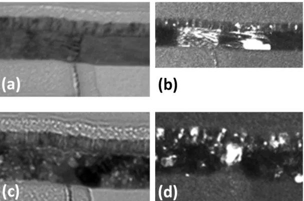
Figure 9 (a) and (b) are bright field and dark field TEM images, respectively, of a cell made using alloy A and in the SET state, while Figures 9(c) and (d) show a cell made using alloy B. Dark field images provide interesting information about the possible conduction paths used by the carriers in the devices. For alloy A, the material is almost monocrystalline from the heater up to the bottom electrode. In alloy B, this region is more complex and consists small crystals.
Figure 9. TEM images of the cells in the SET state. (a) and (c), in bright field;(b) and (d) in dark field.
Figure 10 shows the I(V) characteristics of cells A and B in the SET state, as a function of temperature. Both characteristics are again clearly non-linear but this time somehow different. The overall I(V) characteristics of alloy A appear independent on the temperature while they slightly depend on the temperature for alloy B. Closer inspection shows that the current increases by 12% and 33%, for alloy A and B respectively, when the temperature increases by approximately 150K. Moreover, alloy A enters an exponential regime (constant slope of the current at high fields) after a threshold voltage of 0.2 V, while alloy B exhibits a sub-exponential behavior at high fields. To our knowledge, such characteristics have not been reported so far.
15
Figure 10. I(V) characteristics of the SET state for (a), alloy A and (b), alloy B. (c), R(T) characteristics of SET states for alloy A and alloy B.
Figure 10c shows the variations of the resistances of the cells at low field (V=0.2V). This resistance decrease with increasing temperature tends to point towards an insulating behavior. Being an insulator its resistivity is expected to follow an Arrhenius law, 0. 12345 where Ea, the activation energy is the energetic cost that carriers have to pay in order to take part to conduction. By plotting log(R) as a function of 1/kBT, we obtain by linear regression Ea = 3.6 meV for alloy A and Ea = 12 meV for alloy B. As done for the RESET state, we have analyzed our data by plotting in Figure 11 (a) and (b) the variations of log(I) as a function of the variable q/kBT, at fixed voltages.
16
Figure 11. I(T) characteristics of the SET state for (a,) alloy A and (b), alloy B
These plots evidence that the energy of activation for conduction only slightly depends on the temperature. At contrast, most models used to describe conduction in a GST device in the SET state predict an exponential dependency of the current over the temperature [48] which is clearly not observed here.
Finally, Figure 12 shows the variations of the phase and impedance of the medium as a function of the voltage frequency. Both plots show that the impedances are almost independent on the frequency while the phases only suffer few degrees decreases.
Figure 12. Variations of the impedance and phase as functions of frequency in the SET state for (a), alloy A and (b), alloy B.
This indicates that, in contrast to what has been concluded for the RESET state, the device is mainly resistive and its equivalent electrical circuit should not contain any capacitive element. Thus, from the results obtained by impedance spectroscopy, one could be tempted to label the material as “metallic”, to some extent. This conclusion, in apparent contradiction with the one resulting from the analysis of the I(V) curves, will be discussed in detail in the following.
4. Discussion 4.1 RESET state
The I(V) and I(T) results we have obtained on the cells in the RESET state are quite classical and their general characteristics have already been reported in the literature. Non-linear I(V) characteristics, exponential shaped R(T) curves and energies of activation either linear or proportional to the voltage were indeed already noticed, most often on canonical GST 225. However, impedance spectroscopy has shown new and exclusive results. The phase-shift of the impedance signal down to -90° and the exponential drop
-10 -8 -6 -4 -2 0 0 200 400 600 800 1 000 13,1 13,2 13,3 13,4 13,5 P h a s e ( °) Frequency (kHz) Im p e d a n c e ( kΩ ) Impedance Phase Alloy A -10 -8 -6 -4 -2 0 0 200 400 600 800 1 000 45 46 47 48 49 50 51 P h a s e ( °) Frequency (kHz) Im p e d a n c e ( kΩ ) Impedance Phase Alloy B
17
of the impedance both occurring at high frequency prove the presence of a capacitive element in the equivalent electrical circuits describing the cells in the RESET state. Evidencing a capacitive contribution in GST alloys from impedance spectroscopy measurements has already been reported but, up to now, this characteristic was attributed to the presence of crystalline grains, at least nuclei, resulting from the thermal crystallization of amorphous GST [34-36].
This interpretation cannot hold for our cells. As shown in Figure 1, the material through which the current passes in the RESET state is amorphous, and all along the conduction path for alloy A. However, amorphous does not necessarily means homogeneous in composition. Agati et al. [37], [49] have recently reported how Ge-rich GST alloys decompose in the amorphous phase then form stable Ge and GST 225 crystals upon annealing. From thermodynamics, it is probable that phase segregation survives after melting and multiple cycling of the device and this has been demonstrated experimentally even in the stoichiometric GST-225 [50], [51]. We then suspect that the capacitive behavior we have evidenced is also related to chemical non-homogeneities in the amorphous dome of the cells in the RESET state. For this reason, we have tried to interpret our I(V) and I(T) results by considering not only the often used Poole-Frenkel models but also “granular” models, i.e. models able to describe transport in heterogeneous media, as suggested from our impedance results. However, we have shown that it is not possible to discriminate between different conduction modes by fitting only of the I(V) and I(T) data with the models. All models can reasonably fit the data although they rely on very different physical assumptions. The validity and pertinence of the parameters extracted from the fits are difficult to judge, some having to be set at arbitrary values (for instance, the energy band offset between the grains and the matrix), but still some comments can be done. Actually, the activation energy extracted from the granular models well corresponds to the one directly extracted from the experimental results. The dimensions of the “grains” are reasonable and overall these granular models deserve consideration. Within the framework of this model, the amorphous material in the dome would be made of conductive regions separated from each other by some more resistive material. The overall resistivity of the granular material would result from the capacity of the carriers to hop from one such conductive region to the next, along current paths between the two electrodes.
Finally, we have to discuss the influence of the Ge content onto the characteristics of our GST layers. We have found that the activation energy for conduction is about the same at low field in the two alloys, although their field dependences are different. The resistance and the capacitance of the cell decrease when the Ge content increases. In a granular model, this indicates that the insulating regions separating the conductive grains are thinner and/or less numerous along the conduction path. Actually the composition of alloy A is such that, after phase separation, the Ge phase is in minority while it is in majority in alloy B. Thus, our results can be understood as being due to the transport through a heterogeneous medium consisting of small conductive regions or “grains”, probably of degenerated Ge, separated from each other by small region of more resistive GST in the amorphous state.
4.2 SET state
In the literature, it is generally assumed that cells in the SET state shows a metallic behavior. A metal should give rise to pure and linear ohmic I(V) characteristics while we have shown that they are clearly non-linear. Moreover, although the resistance at low field is much smaller than in the RESET state, it decreases with increasing temperature, a characteristic classically ascribed to insulators and semiconductors. Actually, the I(T) curves somehow challenge this conclusion by showing that the energy of activation for the transport only slightly depends on temperature. Most importantly and at contrast to many previous reports [33]-[36], our impedance spectroscopy results clearly show that the cells in the SET state behave like pure resistances (or involve very small capacitances). To our knowledge, this is the first report of this kind.
All these observations can nevertheless be unified under the hypothesis that conduction takes place through the emission of carriers from defects energetically located very close to one of the bands. This is the hypothesis of Pirovano et al. [41]: in the SET state, the GST is crystalline and the Fermi level is located very close to the valence band edge, probably because the crystal is highly doped and/or the ionization
18
energy of the defects is small [29, 54]. Vacancies in the GST lattice may lead to the creation of such defects near the top of the valence band [41]. Depending on the composition, the Fermi level is located between the top of the valence band and this band of acceptor defects. If the Fermi level is close enough to the valence band then the holes are allowed to reach the valence band at room temperature even under zero field.
This hypothesis, which can alternatively be adapted to describe electron conduction, is supported by the very small values of the activation energy we have measured and fully explains the limited influence of the temperature T on the current in the range of temperatures we have studied (Figure 11. a and b). Indeed, given that at T = 150K (the lowest temperature studied), E = 3/2kBT = 20 meV, then the thermal energy is high enough to activate conduction by ionizing all the defects located close to one of the two band. For high enough temperatures, conduction in our cells in the SET state resembles to band conduction in a doped semiconductor but the material is formally an insulator.
Finally, we have to stress that the energies of activation for conduction we have measured are very small compared to those reported for crystalline GST materials in the literature. For example, Ielmini et al. [27] have reported an activation energy of about 300 meV for GST-225, a value suggesting that the 0.7 eV bandgap semiconductor hosts large concentrations of middle-gap defects.
The very small activation energy we have measured shows something different and must be related to the heterogeneous and polycrystalline nature of the Ge-rich materials embedded in our cells. Since we know that our Ge-rich materials decompose upon crystallization into pure Ge and GST phases [49], a probable explanation is that conduction in the cells occurs by carrier percolation through the most conductive phase. The smaller resistance found in the cells made of alloy B, richer in Ge than alloy A, suggests it is the Ge phase which supports conduction in the two-phase material. The very small ionization energy of the donor defects provided by Sb doping in Ge (about 10 meV) would nicely explain our results. In conclusion, the SET state shows characteristics similar to those found in a semi-conductor heavily doped with impurities having very small ionization energies, i.e. very similar to a metal.
5. Conclusions
Conduction in the amorphous (RESET) state of GST alloys is generally assumed to occur through trap-assisted mechanisms, as expected in homogeneous insulating materials. In the SET state, it is assumed to be ohmic, as in a metal.
In this work, we have investigated in detail the electrical characteristics of PCM cells built using Ge-rich GST alloys. These alloys are of considerable interest as their crystallization temperatures are higher than in the canonical GST-225 and thus they offer an extended range of possible applications.
Surprisingly and at contrast with previous reports, our impedance measurements reveal that, in the RESET state, while the material is mostly amorphous, the cells show a capacitive behavior. This undermines the hypothesis that the material is homogeneous and that conduction can be described through only trap-assisted mechanisms. While models based on the Poole-Frenkel effect can reproduce the non-linearity of the current over the voltage observed at high fields, we show that models describing conduction in granular media can also reproduce the I(V) and I(T) curves we have obtained. Convincingly, the activation energies found from fitting using such a model are very close to those experimentally measured and the values of the physical parameters extracted from the fits are sound and reasonable. Overall, our results support the hypothesis that conduction takes place in a heterogeneous medium consisting of a high density of conductive grains separated by more resistive interfacial regions (the matrix). The noted influence of the Ge content of the alloys on the electrical characteristics of the cells and the known tendency for Ge-rich GST to decompose into pure Ge and GST phases upon cycling lead us to believe that conduction in the RESET state occurs by carrier hopping between still amorphous Ge grains, probably degenerated, or Ge-rich conductive regions separated by more resistive GST-like amorphous regions.
We have also studied the electrical behavior and characteristics of the SET state of the cells. Often considered as “simply ohmic”, we have shown that they also exhibit non-linear currents at relatively low voltages. Conducting like a metal at room temperature, reacting to temperature like an insulator, SET states actually show characteristics similar to those found in a semiconductor heavily doped with impurities having
19
very small ionization energies. Once again, the influence of the Ge content of the alloys on the resistance of the cells and the known tendency for such Ge-rich alloys to undergo phase separation during crystallization lead us to suspect that the observed transport properties results from carrier transport in a percolated metallic network (actually, a degenerated semiconductor). Noting that the ionization energy of Sb in Ge is about 10 meV, it is possible that the overall characteristics of the Ge-rich GST cells in the SET state we measure are close to those of Sb doped Ge.
Finally, our results and analysis confirm that conduction modes in a material cannot be inferred only from I(V) and I(T) curves, as many physically different models give rise to quite similar mathematical expressions which can always be fitted by some set of parameters. This quest must also rely on complementary information, for example provided by impedance spectroscopy, and a good knowledge of the material characteristics resulting from cycling. As far as Ge-rich alloys are concerned, we have shown that their electrical properties are not those of some defective homogeneous material but instead result from strong chemical heterogeneities found both in the amorphous and crystalline phases.
Acknowledgments
This work was initiated with the financial support of the Labex NEXT (n° ANR-10-LABX-0037) in the framework of the “Programme des Investissements d’Avenir”. It could continue as part of the “Ô-GST Project”, funded by nano2022 and the IPCEI on Microelectronics. We thank Prof. Lionel Calmels, Dr. Raj. Sinharoy and Dr. Marta Agati at CEMES for helpful discussions.
20
References :
[1] M. Wuttig and N. Yamada: Phase-change materials for rewriteable data storage. Nat. Mater. 6, 824 (2007).
[2 W. Wełnic and M. Wuttig: Reversible switching in phase-change materials. Materials today 11, 20 (2008). [3] B. C. Lee, P. Zhou, J. Yang, Y. Zhang, B. Zhao, E. Ipek, O. Mutlu, D. Burger: Phase-Change Technology and the Future of Main Memory. IEEE Micro 30, 131 (2010).
[4] G.W. Burr, M. J. Breitwisch, M. Franceschini, D. Garetto, K. Gopalakrishnan, B. Jackson, B. Kurdi, C. Lam, L. A. Lastras, A. Padilla, B. Rajendran, S. Raoux and R. S. Shenoy: Phase change memory technology. J. Vac. Sci. Technol. B 28, 223-262 (2010).
[5] P. Noé, C. Vallée, F. Hippert, F. Fillot, J.-Y. Raty: Phase-change materials for non-volatile memory devices: from technological challenges to materials science issues, Semicond. Sci. Technol. 33, 013002 (2018).
[6] G. Bruns, P. Merkelbach, C. Schlockermann, M. Salinga, M. Wuttig, T. D. Happ, J. B. Philipp, M. Kund: Nanosecond switching in GeTe phase change memory cells, Appl. Phys. Lett. 95, 043108 (2009).
[7] D. Loke, T. H. Lee, W. J. Wang, L. P. Shi1, R. Zhao, Y. C. Yeo, T. C. Chong, S. R. Elliott: Breaking the Speed Limits of Phase-Change Memory, Science 336, 1566 (2012).
[8] P. Noé, C. Sabbione, N. Bernier, N. Castellani, F. Fillot, F. Hippert: Impact of interfaces on scenario of crystallization of phase change materials, Acta Mater. 110, 142 (2016).
[9] R. Berthier, N. Bernier, D. Cooper, C. Sabbione, F. Hippert, P. Noé: In situ observation of the impact of surface oxidation on the crystallization mechanism of GeTe phase-change thin films by scanning transmission electron microscopy, J. Appl. Phys. 122, 115304 (2017).
[10] I. S. Kim, S.L. Cho, D.H. Im, E.H. Cho, D.H. Kim, G.H. Oh, D.H. Ahn, S.O. Park, S.W. Nam, J.T. Moon and C.H. Chung: High performance PRAM cell scalable to sub-20nm technology with below 4F2 cell size, extendable to DRAM applications (Symp. on VLSI Tech. Dig., IEEE, 2010), p. 203.
[11] V. Sousa and G. Navarro: Material engineering for PCM devices optimisation in Phase Change Memory—Device physics, Reliability and Applications (Cham: Springer) chapter 8 (2017).
[12] M. Aoukar: Dépôt de matériaux à changement de phase par PE-MOCVD à injection liquide pulsée pour des applications mémoires PCRAM (PhD Thesis, University of Grenoble Alpes, 2015).
[13] M. Coué: Electrical characterization & TEM analyses of the physical mechanisms governing reliability of Ge-rich Phase-Change Memories (PhD Thesis, University of Grenoble Alpes, 2016).
[14] A. Kiouseloglou: Caractérisation et conception d’architectures basées sur des mémoires à changement de phase, (PhD Thesis, University of Grenoble Alpes, 2015).
[15] P. Zuliani et al., Overcoming Temperature Limitations in Phase Change Memories With Optimized GexSbyTez IEEE TRANSACTIONS ON ELECTRON DEVICES, VOL. 60, NO. 12, DECEMBER 2013 [16] Buscemi, F., Piccinini, E., Brunetti, R., Rudan, M. & Jacoboni, C. Monte Carlo simulation of charge transport in amorphous chalcogenides. J. Appl. Phys. 106, 103706 (2009).
[17] Ambegaokar, V., Cochran, S. & Kurkijärvi, J. Conduction in Random Systems. Phys. Rev. B 8, 3682– 3688 (1973).
[18] Lee, S. et al. Trap-limited and percolation conduction mechanisms in amorphous oxide semiconductor thin film transistors. Appl. Phys. Lett. 98, 203508 (2011).
[19] Murgatroyd, P. N. Theory of space-charge-limited current enhanced by Frenkel effect. J. Phys. Appl. Phys. 3, 151–156 (1970).
[20] Nardone, M., Simon, M., Karpov, I. V. & Karpov, V. G. Electrical conduction in chalcogenide glasses of phase change memory. J. Appl. Phys. 112, 071101 (2012).
[21] M. Simon, M. Nardone, S. A. Kostylev, I. V. Karpov, V. G. Karpov Charge Transport in Nanoglasses of Phase-Change Memory Mater. Res. Soc. Symp. Proc. Vol. 1251 © 2010 Materials Research Society [22] Martin Coué, Electrical characterization & TEM study of the physical mechanisms implied in reliability issues of Ge-rich GST phase-change memories. PhD Thesis, Univ. de Grenoble, 2016
[23] Gallo, M. L., Kaes, M., Sebastian, A. & Krebs, D. Subthreshold electrical transport in amorphous phase-change materials. New J. Phys. 17, 093035 (2015).
21
[24] Betti Beneventi, G., Guarino, L., Ferro, M. & Fantini, P. Three-dimensional Poole-Frenkel analytical model for carrier transport in amorphous chalcogenides. J. Appl. Phys. 113, 044506 (2013).
[25] Abdel-Wahab, F. & Yelon, A. Meyer-Neldel rule and Poole-Frenkel effect in chalcogenide glasses. J. Appl. Phys. 114, 023707 (2013).
[26] Schroeder, H. Poole-Frenkel-effect as dominating current mechanism in thin oxide films—An illusion?! J. Appl. Phys. 117, 215103 (2015).
[27] Ielmini, D. & Zhang, Y. Analytical model for subthreshold conduction and threshold switching in chalcogenide-based memory devices. J. Appl. Phys. 102, 054517 (2007).
[28] Ielmini, D. & Zhang, Y. Evidence for trap-limited transport in the subthreshold conduction regime of chalcogenide glasses. Appl. Phys. Lett. 90, 192102 (2007).
[29] Redaelli, A. Phase change memory: device physics, reliability and applications. (2018).
[30] Frenkel, J. On Pre-Breakdown Phenomena in Insulators and Electronic Semi-Conductors. Phys. Rev. 54, 647–648 (1938).
[31] Hill, R. M. Poole-Frenkel conduction in amorphous solids. Philos. Mag. 23, 59–86 (1971).
[32] N. F. Mott, E. A. Davis. Electronic Processes in on-Crystalline Materials. Krist. Tech. 7, K55–K56 (1972).
[33] Chen, C. et al. Dielectric properties of amorphous phase-change materials. Phys. Rev. B 95, (2017). [34] Huang, Y.-H., Huang, Y.-J. & Hsieh, T.-E. A study of phase transition behaviors of chalcogenide layers using in situ alternative-current impedance spectroscopy. J. Appl. Phys. 111, 123706 (2012).
[35] R.Bez, S.Bossi, B.Gleixner*, F.Pellizzer, A.Pirovano, G.Servalli, M.Tosi "Phase Change Memory development trends," 2010 IEEE International Memory Workshop, Seoul, 2010, pp. 1-4.
[36] Gurinder Singh • Aman Kaura • Monika Mukul •S. K. Tripathi. Electrical, optical, and thermal properties of Sn-doped phase change material Ge2Sb2Te5, J Mater Sci (2013) 48:299–303 DOI 10.1007/s10853-012-6745-z
[37] Agati, M., Renaud, F., Benoit, D. & Claverie, A. In-situ transmission electron microscopy studies of the crystallization of N-doped Ge-rich GeSbTe materials. MRS Commun. 8, 1145–1152 (2018).
[38] Wang, J.-J., Xu, Y.-Z., Mazzarello, R., Wuttig, M. & Zhang, W. A Review on Disorder-Driven Metal– Insulator Transition in Crystalline Vacancy-Rich GeSbTe Phase-Change Materials. Materials 10, 862 (2017).
[39] Volker, H., Jost, P. & Wuttig, M. Low-Temperature Transport in Crystalline Ge1 Sb2Te4. Adv. Funct. Mater. 25, 6390–6398 (2015).
[40] Ielmini, D., Lacaita, A. L., Pirovano, A., Pellizzer, F. & Bez, R. Analysis of Phase Distribution in Phase-Change Nonvolatile Memories. IEEE Electron Device Lett. 25, 507–509 (2004).
[41] Pirovano, A., Lacaita, A. L., Benvenuti, A., Pellizzer, F. & Bez, R. Electronic Switching in Phase-Change Memories. IEEE Trans. Electron Devices 51, 452–459 (2004).
[42] Manuel Le Gallo, Abu Sebastian, Martin Salinga, and Daniel Krebs, High-field electrical transport in amorphous phase-change materials, Matthias Kaes, Journal of Applied Physics 118, 135707 (2015). [43] Giovanni Betti Beneventi, Lucrezia Guarino, Massimo Ferro, and Paolo Fantini Three-dimensional Poole-Frenkel analytical model for carrier transport in amorphous Chalcogenides Citation: Journal of Applied Physics 113, 044506 (2013); doi: 10.1063/1.4788798
[44] H. Nesser, J. Grisolia, T. Alnasser, B. Viallet and L. Ressier. Towards wireless highly sensitive capacitive strain sensors based on gold colloidal nanoparticles Nanoscale, 2018, DOI: 10.1039/C7NR09685B Nanoscale, 2018, 10, 10479 - 10487
[45] A. Zabet-Khosousi. Charge Transport in Self-Assembled Nanoparticle–Molecule Systems. (University of Toronto, 2009).
[46] Stallinga, P. Electronic Transport in Organic Materials: Comparison of Band Theory with Percolation/(Variable Range) Hopping Theory. Adv. Mater. 23, 3356–3362 (2011).
[47] Arnett, P. C. & Klein, N. Poole−Frenkel conduction and the neutral trap. J. Appl. Phys. 46, 1399–1400 (1975).
22
[48] T. Siegrist, P. Jost, H. Volker, M. Woda, P. Merkelbach, C. Schlockermann and M. Wuttig, Disorder-induced localization in crystalline phase-change materials, Nature Materials volume 10, pages 202–208 (2011).
[49] Agati et al., Chemical phase segregation during the crystallization of Ge-rich GeSbTe alloys, J. Mater. Chem. C, 2019, 7, 8720 (2019).
[50] Bong-Sub Lee, Kristof Darmawikarta, Simone Raoux, Yen-Hao Shih, Yu Zhu, Stephen G. Bishop, and John R. Abelson. Distribution of nanoscale nuclei in the amorphous dome of a phase change random access memory. Applied Physics Letters 104, 071907 (2014); doi: 10.1063/1.4865586.
[51] Bong-Sub Lee, Robert M. Shelby, Simone Raoux, Charles T. Retter, Geoffrey W. Burr, Stephanie N. Bogle, Kristof Darmawikarta, Stephen G. Bishop, and John R. Abelson. Nanoscale nuclei in phase change materials: Origin of different crystallization mechanisms of Ge2Sb2Te5 and AgInSbTe. Journal of Applied Physics 115, 063506 (2014); doi: 10.1063/1.4865295.
[52] M. Nardone, M. Simon, I. V. Karpov, and V. G. Karpov Electrical conduction in chalcogenide glasses of phase change memory, (page 11 du PDF, section IV.A, § 7).
[53] Ki-Bong Song, Sang-Su Lee, Kyung-Am Kim, Jeong-Dae Suh, Jun-Ho Kim, Taek-Sung Lee, Byung-ki Cheong, and Won-Mock Kim Undoped homojunction chalcogen thin-film transistors on glass Appl. Phys. Lett. 90, 263510 (2007); https://doi.org/10.1063/1.2753102.
[54] Adler, D. & Yoffa, E. J. Electronic Structure of Amorphous Semiconductors. Phys. Rev. Lett. 36, 1197– 1200 (1976).